

Page 1
MEMS demonstration board based on the LPR410AL
Features
■ Two different working modes:
– analog (AWM)
– digital (DWM)
■ RoHS compliant
Description
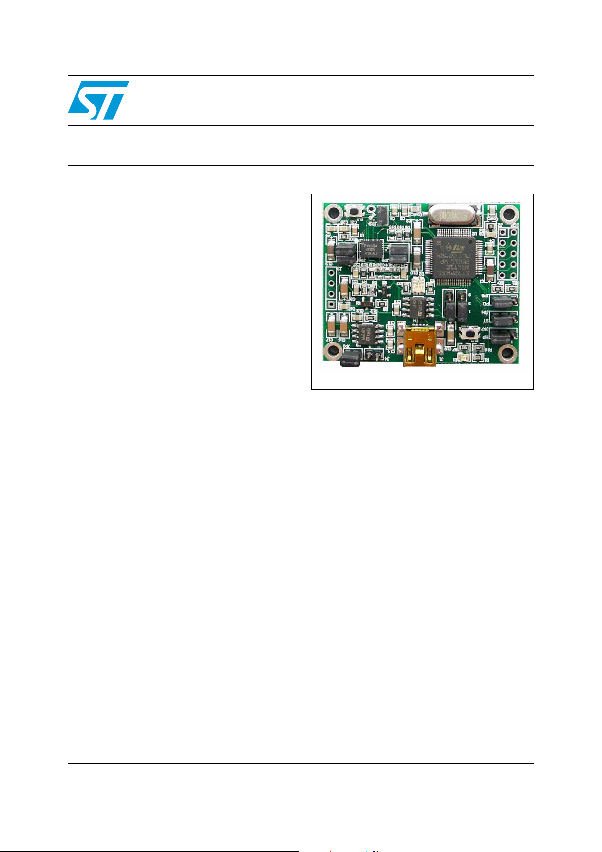
The STEVAL-MKI080V1 demonstration board is
designed to provide the user with a complete,
ready-to-use platform for demonstration of the
LPR410AL product family.
STEVAL-MKI080V1
analog output 2-axis gyroscope
Data brief
The STEVAL-MKI080V1 includes a sensing
element and an IC interface capable of translating
information from the sensing element into a
measured signal that can be used for external
applications.
In addition to the MEMS sensor, the
demonstration board uses an ST7 microcontroller
which functions as a bridge between the sensor
and the PC. This makes it possible to download
the graphical user interface (GUI) from the
website or to use dedicated software routines for
customized applications.
The STEVAL-MKI080V1 demonstration board has
been designed for use in two different working
modes: analog and digital.
In analog mode (AWM) the microcontroller is
disabled and the analog outputs of the device are
available to the user on a dedicated connector.
This is the default working mode when power is
supplied through either the USB connector or the
supply connector.
In digital mode (DWM) the microcontroller is
enabled and allows the user to digitally acquire
the output signals of the device, to view them on
the PC through the dedicated GUI, and to
manage the control pins of the device.
STEVAL-MKI080V1
March 2011 Doc ID 018524 Rev 1 1/5
For further information contact your local STMicroelectronics sales office.
www.st.com
5
Page 2
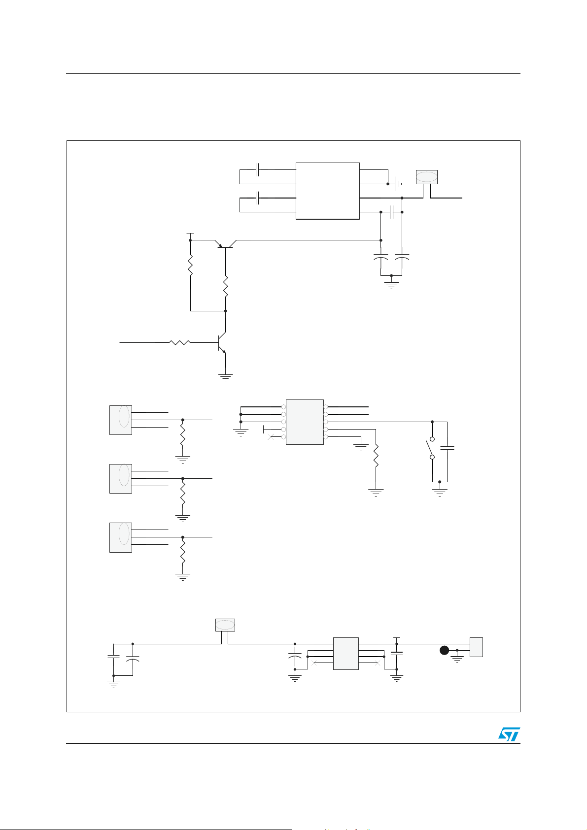
Schematic diagrams STEVAL-MKI080V1
1 Schematic diagrams
Figure 1. STEVAL-MKI080V1 circuit schematics (1 of 2)
JP4
ST
JP5
PD
DFU _SEL
3
2
1
3
2
1
ST_u
Vddf
PD_u
Vddf
R8
1K
R4
10K
VCC
R11
10K
R17
10K
2
ST
PD
Q1
2STR2215
2
R5
47 0R
31
Q2
SO642
31
VCC
220nFC14
1
2
3
220n FC15
4
J2
1
3
5
7
9 10
ICP
C1-
C1+
C2-
C2+
ST662ABD
2
4
6
8
U3
SHDN
GND
VOUT
VCC
C16
4. 7uF16V
iccdata
iccclk
nRE SET
iccsel
8
7
6
JP2
1
2
iccsel
5
C12
100nF
+
+
C17
4. 7uF16V
R12
10K
SW1
NReset
C7
100nF
JP7
HP
C11
100n F
HP_ u
3
2
Vddf
1
C13
+
10uF
HP
R16
10K
JP3
Current_Measure
1
2
Vdd_ dutVddf
C18
2. 2uF
2/5 Doc ID 018524 Rev 1
U4
1
2
+
3
4
1
2
3
4
LE30 CD
8
7
6
5
VCC
8
7
6
5
C19
100n F
TP2
J4
1
2
Power Supply
GAPMSMD00007
Page 3

STEVAL-MKI080V1 Schematic diagrams
Figure 2. STEVAL-MKI080V1 circuit schematics (2 of 2)
D1
J1
V+
DM
DP
nc
GND
USB_mini_B
R1
180R
1
2
3
4
5
VCC
C1
C4
10 0nF
C2
+10uF
C5
+4.7uF
10 0nF
TP1
TP3
OSCIN
ic cdata
ic cclk
Vddf
62
57
56
60
58
Vss a61Vss 2
Vdd259Vdda
ICCCLK
ICCDATA
nR ESET
ic csel
49
50
51
53
52
55
SCL
SDA
AIN054AIN1
USBEN
RESET
Vpp/ICCSEL
OCMP 2
OCMP 1
R6
1. 5K
C8
47nF
C9
220n F
C10
+10uF
Vddf
Rled
Gle d
DFU _SEL
oscin
oscout
63
64
1
UVss
2
3
4
5
6
7
8
9
10
11
12
13
14
15
16
UDM
UDP
UVc c
UVdd
Vddf
Vssf
PE5
PE6
PE7
PB0
PB1
PB2
PB3
PB4
PB5
OSCOUT
U2
ST72F 651A R6T1 E
PWM1
PWM0
AIN 6
AIN 5
AIN 4
AIN 3
AIN 2
PD3
PD2
PD1
PD0
PC7
PC6
PC5
PC4
Cosc1
33pF
48
47
46
45
44
43
42
41
40
39
38
37
36
35
34
33
oscin oscout
Yoscm
Cosc2
33pF
4xOu t1
Out1
4xOu t2
Out2
Vref
12MHz
OutAna1
OutAna2
Vddf
R2
R3
100R
100R
D2
GR
RledGl ed
3
2
1
JP1
3
2
1
JP6
PB617PB718PA019PA120PA221PA322PA423PA524PA625PA726SS27MISO28MOSI29SCK30Vdd131Vss 1
C3
4. 7uF
VCC
OutA na1
OutA na2
+
C6
100n F
Vref
123
4
J3
R7
10K
32
PD_u
HP_u
Vddf
ST_u
SW2
R10
C20
10K
470n F
FILTVDD
10nF
C25
33nF
R13
33K
Vref
C21
R14
DN M
R18
0R
VCO NT
JP8
12
34
1
2
3
4
5
6
Out1
C26
tbd
No t Mo unted
ST
PD
27
26
28
ST
PD
OUTX
GND
NC
NC
NC
4xI N_X
NC
4xOU TX7NC8Vdd9NC10NC11NC12NC134xOU TY
Vdd_dut
4xOu t1
HP
Vref
25
24
HP
Res
U1
21
23
22
NC
NC
Vref
OUTY
FILTVDD
VCO NT
4xI N_Y
Vdd
20
19
18
17
Vdd_ dut
FILTVDD
VCO NT
1
3 4
JP9
16
15
NC
R19
0R
2
R15
DNM
R9
33 K
C24
33nF
Vref
Out2
14
C27
tbd
4xOu t2
No t Mo unted
GAPMSMD00008
Doc ID 018524 Rev 1 3/5
Page 4

Revision history STEVAL-MKI080V1
2 Revision history
Table 1. Document revision history
Date Revision Changes
04-Mar-2011 1 Initial release.
4/5 Doc ID 018524 Rev 1
Page 5

STEVAL-MKI080V1
Please Read Carefully:
Information in this document is provided solely in connection with ST products. STMicroelectronics NV and its subsidiaries (“ST”) reserve the
right to make changes, corrections, modifications or improvements, to this document, and the products and services described herein at any
time, without notice.
All ST products are sold pursuant to ST’s terms and conditions of sale.
Purchasers are solely responsible for the choice, selection and use of the ST products and services described herein, and ST assumes no
liability whatsoever relating to the choice, selection or use of the ST products and services described herein.
No license, express or implied, by estoppel or otherwise, to any intellectual property rights is granted under this document. If any part of this
document refers to any third party products or services it shall not be deemed a license grant by ST for the use of such third party products
or services, or any intellectual property contained therein or considered as a warranty covering the use in any manner whatsoever of such
third party products or services or any intellectual property contained therein.
UNLESS OTHERWISE SET FORTH IN ST’S TERMS AND CONDITIONS OF SALE ST DISCLAIMS ANY EXPRESS OR IMPLIED
WARRANTY WITH RESPECT TO THE USE AND/OR SALE OF ST PRODUCTS INCLUDING WITHOUT LIMITATION IMPLIED
WARRANTIES OF MERCHANTABILITY, FITNESS FOR A PARTICULAR PURPOSE (AND THEIR EQUIVALENTS UNDER THE LAWS
OF ANY JURISDICTION), OR INFRINGEMENT OF ANY PATENT, COPYRIGHT OR OTHER INTELLECTUAL PROPERTY RIGHT.
UNLESS EXPRESSLY APPROVED IN WRITING BY AN AUTHORIZED ST REPRESENTATIVE, ST PRODUCTS ARE NOT
RECOMMENDED, AUTHORIZED OR WARRANTED FOR USE IN MILITARY, AIR CRAFT, SPACE, LIFE SAVING, OR LIFE SUSTAINING
APPLICATIONS, NOR IN PRODUCTS OR SYSTEMS WHERE FAILURE OR MALFUNCTION MAY RESULT IN PERSONAL INJURY,
DEATH, OR SEVERE PROPERTY OR ENVIRONMENTAL DAMAGE. ST PRODUCTS WHICH ARE NOT SPECIFIED AS "AUTOMOTIVE
GRADE" MAY ONLY BE USED IN AUTOMOTIVE APPLICATIONS AT USER’S OWN RISK.
Resale of ST products with provisions different from the statements and/or technical features set forth in this document shall immediately void
any warranty granted by ST for the ST product or service described herein and shall not create or extend in any manner whatsoever, any
liability of ST.
ST and the ST logo are trademarks or registered trademarks of ST in various countries.
Information in this document supersedes and replaces all information previously supplied.
The ST logo is a registered trademark of STMicroelectronics. All other names are the property of their respective owners.
© 2011 STMicroelectronics - All rights reserved
Australia - Belgium - Brazil - Canada - China - Czech Republic - Finland - France - Germany - Hong Kong - India - Israel - Italy - Japan -
STMicroelectronics group of companies
Malaysia - Malta - Morocco - Philippines - Singapore - Spain - Sweden - Switzerland - United Kingdom - United States of America
www.st.com
Doc ID 018524 Rev 1 5/5
 Loading...