

Page 1
.8 INPUT/OUTPUTPINS
• Individually programmable direction
• Individualinterrupt source capability
Programmable edge selection
-
.16 SOURCEINTERRUPTCONTROLLER
• 8 Internal sources
• 8 External sources
• Individualsource enable
• Individualsource masking
• Programmable interrupt service modes
Polling
-
Vectorgeneration
-
OptionalIn-service status
-
• Daisychaining capability
.FOUR TIMERS WITH INDIVIDUALLY PRO-
GRAMMABLE PRESCALING
• Twomultimode timers
Delaymode
-
Pulse width measurement mode
-
Event countermode
-
• Twodelay mode timers
• Independent clockinput
• Timeout output option
.SINGLECHANNEL USART
• Full Duplex
• Asynchronous to 65kbps
• Bytesynchronous to 1 Mbps
• Internal/External baud rate generation
• DMAhandshake signals
• Modemcontrol
• Loop back mode
.68000BUS COMPATIBLE
.48 PIN DIP OR 52 PIN PLCC
MK68901
MULTI–FUNCTION PERIPHERAL
1
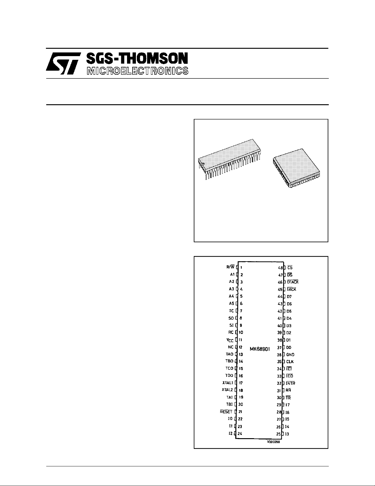
DPIP48 PLCC52
Figure1 : Pin connections.
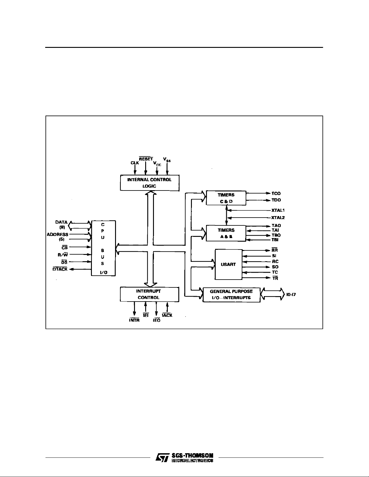
DESCRI PT ION
The MK68901 MFP (Multi-Function Peripheral) is a
combination of many of the necessary peripheral
functions in a microprocessor system.
Included are :
Eight parallel I/O lines
Interrrupt controller for 16 sources
Four timers
Single channelfull duplex USART
The useof the MFPin a system cansignificantly reducechipcount,thereby reducing systemcost. The
MFPiscompletely 68000buscompatible,and24directlyaddressable internal registers providethe ne-
December1988
MFP
1/33
Page 2

MK68901
necessary control and status interface to the programmer.
The MFP is a derivative of the MK3801 STI, a Z80
familyperipheral.
PIN DESCRIPTION
GND : Ground
VCC: +5 volts (± 5%)
CS : Chip Select (input, active, low). CS is u-
sed toselect the MK68901 MFP for accessesto the internal registers. CS and
IACK must not be asserted at the same
time.
DS : Data Strobe (input, active low). DS is u-
sedaspartofthechipselectandinterrupt
acknowledge functions.
R/W : Read/Write (input). R/W is the signal
from the bus master indicating whether
thecurrent bus cycle is a Read (High) or
Write (Low) cycle.
DTACK: DataTransfer Acknowledge. (output,ac-
tive low, tri-stateable) DTACK is used to
signalthebus master that data is ready,
or that data has been accepted by the
MK68901 MFP.
A1-A5 : Address Bus (inputs).The adress bus is
used to adress one of the internal registersduring a read or write cycle.
D0-D7 : Data Bus (bi-directional, tri-stateable).
Thedatabusisusedtoreceive datafrom
or transmit data to one of the internal registers during a read or write cycle. It is
also used to pass a vector during an interruptacknowledge cycle.
CLK : Clock (input). This input is used to pro-
vide the internal timing for theMK68901
MFP.
RESET: Device reset. (input, active low). Reset
disablesthe USART receiver and transmitter,stops all timers and forcesthe timer outputs low, disables all interrupt
channels and clears any pending interrupts.The General PurposeInterrupt/I/O
lines will be placed in the tri-state input
mode.Allinternal registers (except the timer,USART dataregisters, and transmit
status register) will be cleared.
INTR : Interrupt Request (output, active low, o-
pen drain). INTR is asserted when the
MK68901 MFP isrequesting aninterrupt.
INTR is negated during an interrupt ac-
knowledge cycle or by clearing the pending interrupt(s) throughsoftware.
IACK: Interrupt Acknowledge (input, active
low).IACKisusedtosignaltheMK68901
MFP that the CPU is acknowledging an
interrupt. CS and IACk must not be assertedat the same time.
IEI : Interrupt Enable In (input,active low). IEI
is used to signal the MK68901 MFP that
no higherpriority device is requesting interrupt service.
IEO : InterruptEnable Out (output, active low).
IEO is used to signal lower priority peripherals that neither the MK68901 MFP
nor another higher priority peripheral is
requesting interrupt service.
10-17 : General Purpose Interrupt I/O lines.
Theselines may be used as interrupt inputs and/or I/O lines. When used as interrupt inputs, their active edge is programmable. A datadirection registerisused to define which lines are to be Hi-Z
inputsand whichlinesareto bepush-pull
TTL compatible outputs.
SO: SerialOutput.This is the outputof the U-
SART transmitter.
SI : Serial Input. This is the input to the U-
SART receiver.
RC : Receiver Clock. This input controls the
serialbit rate of theUSART receiver.
TC : TransmitterClock.Thisinput controlsthe
serialbit rate of theUSART transmitter.
RR : Receiver Ready. (output, active low)
DMA output for receiver, which reflects
the status of Buffer Full in port number
15.
TR : Transmitter Ready. (output, active low)
DMA output for transmitter, which reflects the status of Buffer Empty in port
number 16.
TAO,TBO,
TCO,TDO:
XTAL1,
XTAL2 :
Timer Outputs. Each of the four timers
has an output which can produce a
square wave. The output will change
stateseach timercycle ; thusone fullperiod of thetimer out signal is equalto two
timer cycles. TAO or TBO can be reset
(logic”O”) by a write to TACR, or TBCR
respectively.
Timer Clock inputs. A crystal can be
connected between XTAL1 and XTAL2,
or XTAL1 can be driven with a TTL level
clock.Whendriving XTAL1 withaTTL le-
2/33
Page 3
MK68901
velclock,XTAL2mustbe allowedtofloat.
Whenusingacrystal,externalcapacitors
are required. See figure 33. All chip accesses are independent of the timer
clock.
TAI,TBI: TimerA,Binputs. Usedwhenrunning the
timers in the event count or the pulse
width measurement mode. The interrupt
channelsassociated with 14 and 13 are
usedforTAIandTBI,respectively.Thus,
when running a timer in the pulse width
V000351
3/33
Page 4

MK68901
Figure 4 : RegisterMap.
Address Port N °. Abbreviation Regi ster Name
0
1
2
3
4
5
6
7
8
9
A
B
C
D
E
F
10
11
12
13
14
15
16
17
GPIP
AER
DDR
IERA
IERB
IPRA
IPRB
ISRA
ISRB
IMRA
IMRB
VR
TACR
TBCR
TCDCR
TADR
TBDR
TCDR
TDDR
SCR
UCR
RSR
TSR
UDR
GENERAL PURPOSE I/O
ACTIVE EDGE REGISTER
DATA DIRECTION REGISTER
INTERRUPT ENABLE REGISTER A
INTERRUPT ENABLE REGISTER B
INTERRUPT PENDING REGISTER A
INTERRUPT PENDING REGISTER B
INTERRUPT IN-SERVICE REGISTER A
INTERRUPT IN-SERVICE REGISTER B
INTERRUPT MASK REGISTER A
INTERRUPT MASK REGISTER B
VECTOR REGISTER
TIMER A CONTROL REGISTER
TIMER B CONTROL REGISTER
TIMERS C AND D CONTROL REGISTER
TIMER A DATA REGISTER
TIMER B DATA REGISTER
TIMER C DATA REGISTER
TIMER D DATA REGISTER
SYNC CHARACTER REGISTER
USART CONTROL REGISTER
RECEIVER STATUS REGISTER
TRANSMITTER STATUS REGISTER
USART DATA REGISTER
IN TERRUP TS
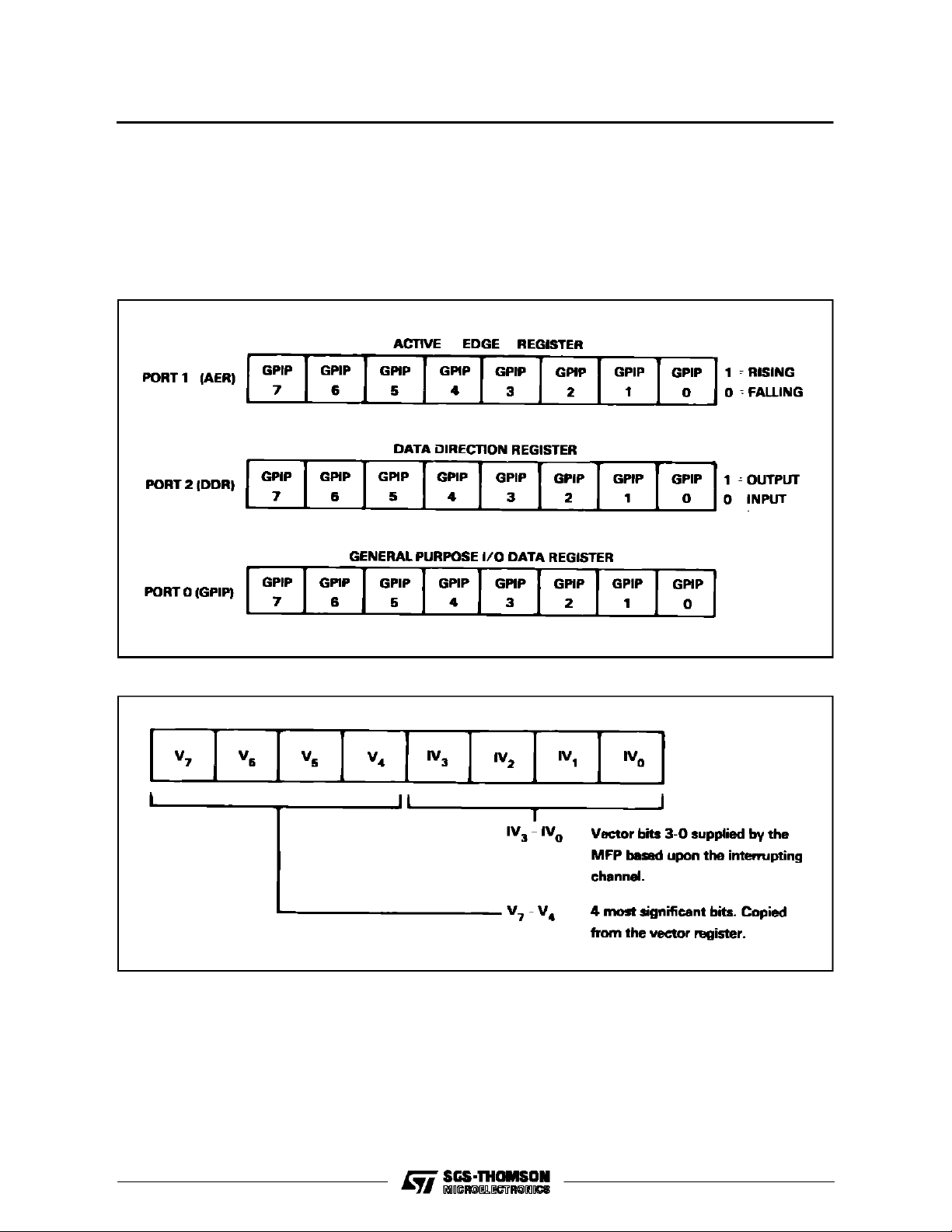
The GeneralPurpose I/O-InterruptPort(GPIP) provides eight I/O lines that may be operated eitheras
inputsor outputsundersoftwarecontrol. In addition,
each line may generate an interrupt in either a positivegoing edge or a negative goingedge ofthe input signal.
The GPIP has three associated registers. One allows the programmer to specify the ActiveEdgefor
eachbitthatwilltrigger an interrupt. Another register
specifies the Data Direction (input or output) associated with each bit. The thirdregister is the actual
data I/O register used to input or output datato the
port. These three registers are illstrated in figure5.
The ActiveEdge Register (AER) allows each of the
General Purpose Interrupts to provide an interrupt
on either a 1-0 transition or a 0-1 transition. Writing
a zero to the appropriate bit of the AER causes the
associatedinput to produce an interrupt on the 1-0
transition. The edgebit is simply one input to an exclusive-orgate, withthe otherinput comingfrom the
input buffer ant the output going to a 1-0 transition
detector. Thus, depending upon the state of the input, writing the AER can cause an interrupt-producing transition,which will cause an interrupt on the
associatedchannel, if that channel is enabled. One
would then normally configure the AER before
enabling interrupts via IERA and IERB.
Note : Changing the edge bit, with the interrupt
enabled, may cause an interrupt on that channel.
TheDataDirection Register(DDR)isusedtodefine
10-17 as inputs or as outputs on a bit by bit basis.
Writinga zero into a bit of the DDR causes the corresponding Interrupt-I/O pin to be a Hi-Z input. Writing a one into a bit of the DDR causes the corresponding pin to be configured as a push-pull output. When data is written into the GPIP,those pins
definedas inputs willremainin theHi-Z state while
those pins definedas outputs will assume the state
(high or low) of their corresponding bit in the GPIP.
When the GPIP is read, the data readwill come directlyfromthecorresponding bitoftheGPIPregister
forallpinsdefinedas output, whilethe data read on
all pins defined as inputs will come from the input
buffers.
Eachindividual functionin the MK68901isprovided
withauniqueinterruptvectorthatispresentedtothe
systemduring the interrupt acknowledgecycle.The
interrupt vector returned during the interrupt acknowledge cycleis shownin figure 6,whilethe vectorregisteris shown in figure7.
4/33
Page 5
MK68901
There are 16 vectoraddresses generated internally
by the MK68901, one for each of the 16 interrupt
channels.
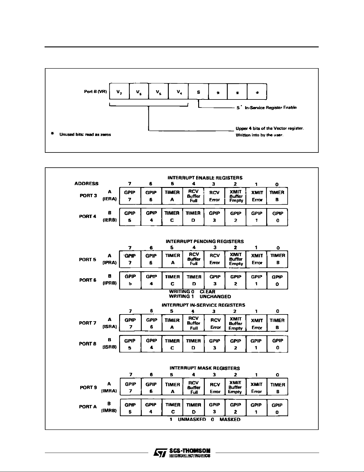
The Interrupt Control Registers (figure 8) provide
controlof interrupt processing for all I/O facilitiesof
the MK68901. These registers allow the program-
Figure 5 : General Purpose I/O Registers.
mer to enable or disable any or all of the 16 interrupts,providing maskingfor any interrupt, and provide accessto the pending and in-service status of
the interrupt. Optional end-of-interrupt modes are
available under software control. All the interrupts
areprioritized as shown in figure 9.
Figure 6 : Interrupt Vector.
V000352
V000353
5/33
Page 6
MK68901
Figure 7 : VectorRegister.
Figure 8 : InterruptControl Registers.
V000354
6/33
V000355
Page 7

Figure 9 : Interrupt Control Register Definitions
Priority Channel Descriptio n
HIGHEST
LOWEST
1111
1110
1101
1100
1011
1010
1001
1000
0111
0110
0101
0100
0011
0010
0001
0000
General Purpose Interrupt 7(I7)
General Purpose Interrupt 6(I6)
Timer A
Receive Buffer Full
Receive Error
Transmit Buffer Empty
Transmit Error
Timer B
General Purpose Interrupt 5(I5)
General Purpose Interrupt 4(I4)
Timer C
Timer D
General Purpose Interrupt 3(I3)
General Purpose Interrupt 2(I2)
General Purpose Interrupt 1(I1)
General Purpose Interrupt 0(I0)
MK68901
Interrupts may be either polled or vectored. Each
channel may be individual enabled or disabled by
writinga one or a zeroin theappropriate bitof Interrupt EnableRegisters (IERA, IERB-seefigure 8for
all registers in this section). When disabled, an interrupt channel is completely inactive. Any internal
or externalaction which would normally produce an
interrupt onthatchannelis ignored and anypending
interrupt onthat channel willbecleared by disabling
that channel.Disabling aninterrupt channel hasno
effect on the corresponding bit in Interrupt In-Service Registers (ISRA, ISRB); thus,if the In-service
Registersare used and an interrupt is in service on
that channelwhenthe channel is disabled, itwillremain in service until cleared in the normal manner.
IERA and IERB are alsoreadable.
When an interrupt is received on an enabled channel, itscorresponding bit in the pending register will
be set. When that channel is acknowledged it will
pass its vector,and thecorresponding bit in the Interrupt Pending Register (IPRA or IRPB) will be
cleared. IPRA and IPRBare readable ; thus by polling IPRA and IPRB, it can be determined whether
a channel has a pending interrupt. IPRA and IPRB
are also writeable and a pending interrupt can be
clearedwithout goingthrough the acknowledge sequence by writing a zero to the appropriate bit.This
allowsanyonebitto becleared, without alteringany
other bits, simply by writing all ones exceptfor the
bit position to be cleared to IPRA or IPRB. Thus a
fully polled interrupt schemeis possible. Note : writing a one to IPRA,IPRB has no effect on the interrupt pending register.
The interrupt maskregisters (IMRAand IMRB)may
beused to blocka channelfrommakingan interrupt
request. Writinga zero intothe corresponding bit of
the mask register will still allow the channel to receive an interrupt and latch it into its pending bit (if
thatchannel is enabled), but willprevent that channelfrom makingan interrupt request. Ifthat channel
is causing an interrupt request at the time the corresponding bit inthe maskregister iscleared, therequest willcease.If no other channel is making a request, INTRwillgo inactive. If the mask bitis re-enabled, any pending interrupt is now free to resume
its request unless blocked by a higher priority requestforservice. IMRAand IMRBarealsoreadable
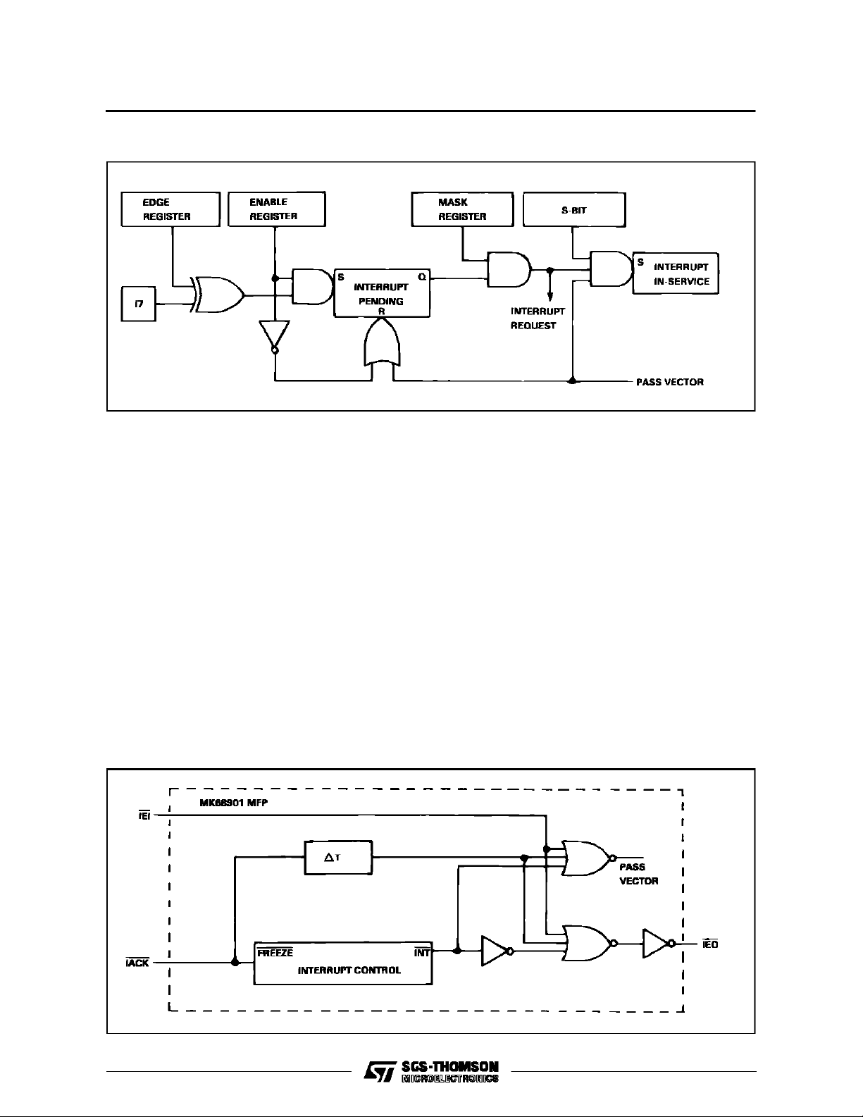
. A conceptual circuit of an interrupt channel is
shownin figure10.
7/33
Page 8
MK68901
Figure 10 : A Conceptual Circuitof an Interrupt Channel.
V000356
Therearetwoend-of-interrupt modes : the automatic end-of-interrupt mode andthesoftwareend-of-interruptmode. Themodeisselected by writinga one
or a zero to the S bit of theVector Register (VR). If
the S bit of the VR is a one, all channels operate in
the software end-of-interrupt mode. If the S bitis a
zero, all channels operate in the automatic end-ofinterrupt mode, and a reset is held on all in-service
bits. In the automatic end-of-interrupt mode, the
pending bit is cleared when that channel passes its
vector. At that point, no further history of that interrupt remains in the MK68901 MFP. In the software
end-of-interrupt mode, the in-service bit is set and
the pending bit is cleared when the channel passes
itsvector.Withthein-service bitset,nolowerpriority
channelisallowed torequest an interrupt or topass
its vector during an acknowledge sequence ; however, a lower priority channelmaystillreceive an interruptand latchit intothepending bit.Ahigher priority channelmay stillrequestan interrupt andbe ac-
knowledged. The in-service bitof a particularchannel may be cleared by writing a zero to the corresponding bit in ISRA or ISRB. Typically, thiswill be
done at the conclusion of the interrupt routine just
before thereturn. Thusno lower priority channelwill
beallowedto requestserviceuntil thehigherpriority
channel is complete, while channels of still higher
priority will be allowed torequest service. While the
in-service bit isset,a secondinterrupt on that channelmaybereceivedandlatched intothependingbit,
though no service request will be made in response tothesecond interrupt untilthein-service bit
iscleared. ISRA and ISRB mayberead atany time.
Only a zero may be writtenintoany bit of ISRA and
ISRB;thusthein-servicebitsmaybe cleared insoftwarebut cannotbe set insoftware.This allows any
onebit tobe cleared, without alteringany other bits,
simplyby writingall ones except for the bit position
to be cleared to ISRA or ISRB, as with IPRA and
IPRB.
Figure 11 a : A Conceptual Circuit of the MK68901 MFP Daisy Chaining.
8/33
V000357
Page 9
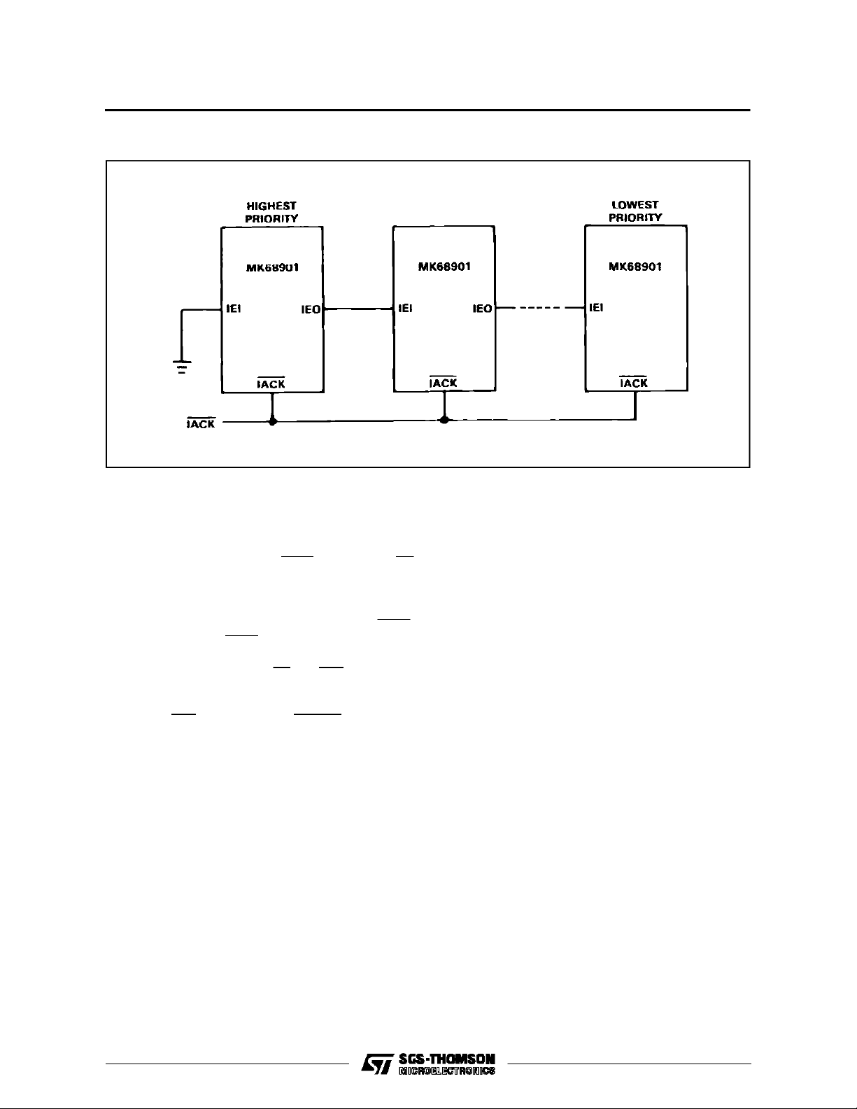
Figure 11 b : Daisy Chaining.
MK68901
V000358
Each interrupt channel respondswith a discrete 8bit vector when acknowledged. The upper four bits
of the vector are setby writing the upper four bits of
the VR.The four low order bits (bit 3-bit 0) are generatedby the interrupting channel.
Toacknowledge aninterrupt, IACKgoeslow,theIEI
inputmustgolow (or be tiedlow)and the MK68901
MFPmust have an acknowledgeable interrupt pending. The Daisy Chaining capability (figure 11) requires that allpartsin achainhaveacommonIACK.
Whenthe common IACK goes low, all parts freeze
and prioritize interrupts in parallel. Then priority is
passeddownthe chain, via IEI and IEO, untila part
which has a pending interrupt is reached. The part
withthepending interrupt, passesa vector,doesnot
propagate IEO, and generatesDTACK.
Figure 9 describes the 16 prioritized interrupt channels.Aschown, GeneralPurpose Interrupt7hasthe
highestpriority, whileGeneralPurpose Interrupt 0 is
assignedthe lowestpriority. Eachofthesechannels
may be reprioritized, in effect, by selectively masking interrupts under software control. The binary
numbers under ”channel” correspond to the modified bits IV3, IV2, IV1 and IV0, respectively, of the
InterruptVector for each channel (see figure 6).
Each channel has an enable bit contained in IERA
or IERB, a pending latchcontained in IPRAor IPRB,
a maskbit contained in IMRA or IMRB, and an in–
servicelatch contained inISRAor ISRB. Additionally, the eight General Purpose Interrupts each have
an edge bit contained in the Active Edge Register
(AER), a bit to define the line as input or output
contained intheData Direction Register(DDR)and
an I/O bit in the General PurposeInterrupt-I/O Port
(GPIP).
TIMERS
Therearefour timerson theMK68901 MFP. Twoof
thetimers (Timer A and Timer B) arefullfunction timers which can perform the basic delay function
and can also perform event counting, pulse width
measurement, and waveformgeneration. Theother
two timers (Timer C and Timer D) are delay timers
only.Oneorbothofthesetimers canbeusedtosupply the baud rate clocks for the USART. All timers
are prescaler/counter timers with a common independent clockinput(XTAL1, XTAL2). Inaddition, all
timershave a time-out output, function that toggles
eachtime the timer times out.
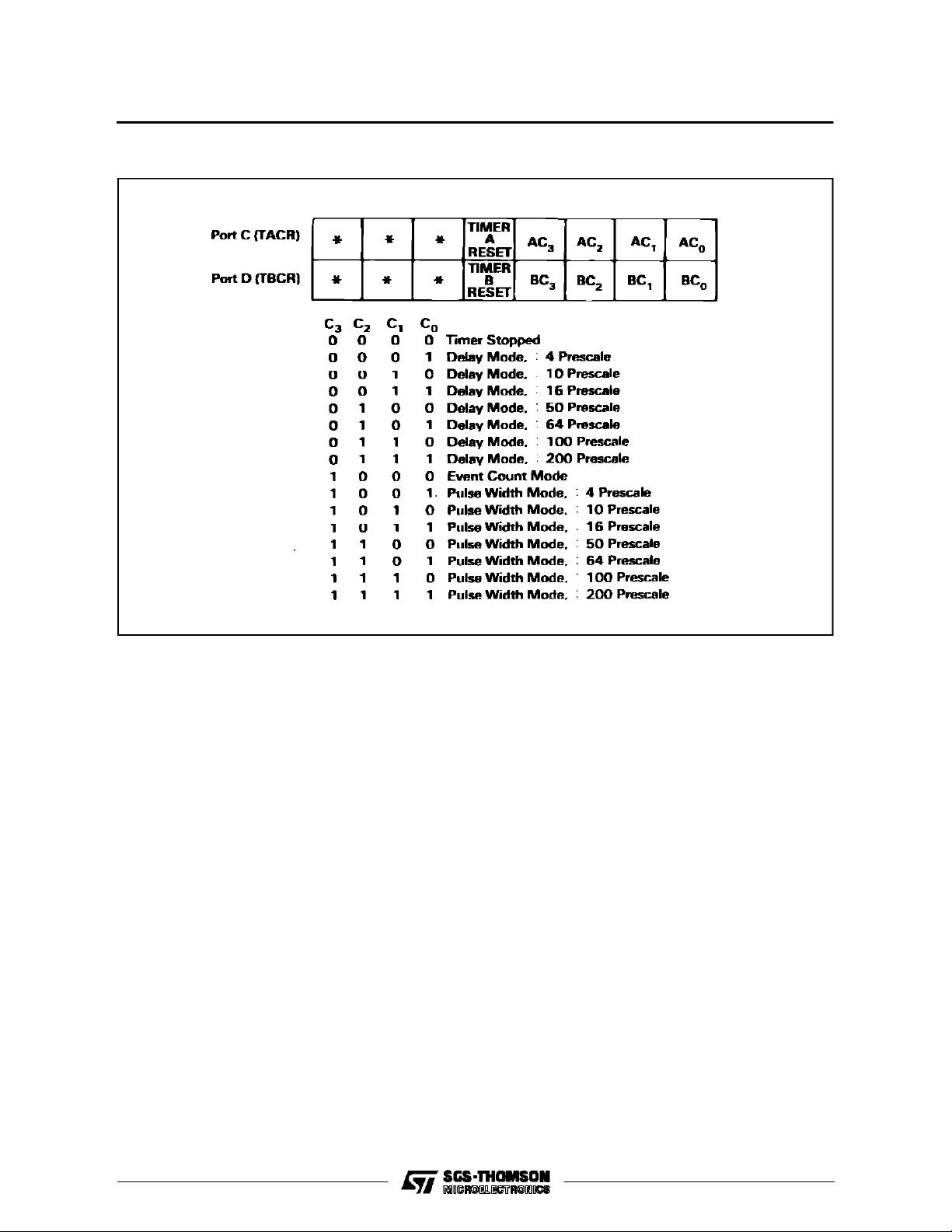
The four timers are programmed via three Timer
ControlRegisters andfourTimerDataRegisters.Timers A and Bare controlledby thecontrol registers
TACRand TBCR,respectively (see figure 12), and
by the data registers TADR and TBDR (figure 13).
TimersCand Darecontrolled bythecontrolregister
TCDCR (see figure 14) and two data registers
TCDR and TDDR. Bits in the control registers allow
the selection of operational mode, prescale, and
controlwhite the data registers are usedto read the
timeror write into the time constant register. Timer
A and B input pins TAI and TBI, are used for the eventand pulse width modes for timers A andB.
Withthe timer stopped, no counting can occur.The
timercontents will remainunaltered while the timer
isstopped(unlessreloaded bywriting the TimerDataRegister), but any residualcount in the prescaler
willbe lost.
9/33
Page 10
MK68901
Figure 12 : Timer A and B Control Registers.
Unused bits : read as zeros.
*
In the delay mode, the prescaler is always active.
A countpulse will be applied to the main timer unit
each time the prescribed number of timer clock cycles has elapsed. Thus, if the prescaler is programmed to divide by ten, a count pulse will be applied
to the main counter every ten cycles of the timer
clock.
Eachtimeacount pulseisapplied tothemaincounter, it will decrement its contents. The main counter
is initiallyloadedby writingto theTimer Data Register. Each count pulsewillcause the current countto
decrement. When the timerhasdecremented down
to ”01” , the next countpulsewill not cause it to decrement to ”00”. Instead, the next count pulse will
cause the timerto bereloaded from the Timer Data
Register.Additionally, a ”Timeout” pulse willbeproduced. This Time Out pulse is coupled to the timer
interrupt channel, and, if thatchannel is enabled,an
interrupt willbe produced. TheTime Outpulseis also coupled to the timeroutput pin and willcausethe
pin to change states.The output will remain in this
newstateuntilthenextTimeOutpulseoccurs. Thus
the output will complete one full cycle for each two
Time Out pulses.
If, for example, the prescaler were programmed to
divideby ten,andthe TimerData Register wereloa-
V000359
ded with 100(decimal),the main counter would decrement onceforeverytencyclesofthe timerclock.
ATimeOutpulsewilloccur(henceaninterrupt ifthat
channel is enabled) every 1000 cycles of the timer
clock,and thetimer outputwill complete one fullcycleevery 2000 cyclesof thetimer clock.
The maincounter is an 8-bit binary down counter. It
maybe readat any time by reading theTimer Data
Register. The information read is the information
lastclockedintothetimerreadregister when the DS
pinhadlastgonehigh prior to thecurrentreadcycle.
When written,dataisloaded intotheTimerDataRegister,and the main counter, if the timeris stopped.
If the Timer Data Register is written while the timer
is running, thenewwordis notloaded intothe timer
until it counts through H”01”. However, if the timer
iswritten whileitis counting throughH”01”,an indeterminatevalue willbewrittenintothetimer constant
register. This maybecircumvented byensuringthat
the data register is not written when the count is
H”01”.
If the main counter is loaded with ”01”, a Time Out
Pulse will occur every time the prescaler presents
a count pulse to the main counter. If loaded with
”00”, a Time Out pulse will occur every 256 count
pulses.
10/33
Page 11

Figure 13 : Timer Data Registers (A, B, C, andD).
Figure 14 : Timer C and D Register.
MK68901
V000360
Unused bits : re ad as zeros.
*
V000361
11/33
Page 12

MK68901
Figure 15 : A Conceptual Circuitof theMFP Timers in the Pulse Width Measurement Mode.
Changing the prescale value with the timer running
can causethe firstTimeOut pulse tooccurat an indeterminate time, (no less thanone nor more than
200 timer clockcycles timesthe number in the time
constantregister),but subsequent Time Out pulses
will then occur at thecorrect interval.
In addition to the delay mode described above, Timers A and B can also function in the Pulse Width
Measurement mode orin the EventCount mode.In
eitherofthesetwomodes,anauxiliary controlsignal
is required. Theauxiliary control input forTimer A is
TAI,andforTimerB,TBIisused.Theinterrupt channels associatedwith14 and13 are used forTAIand
TBI, respectively, in Pulse Width mode. See Figure
15.
The pulse width measurement mode functions
much like the delay mode. However, in this mode,
the auxiliary control signal on TAIor TBI acts as an
enableto the timer. When the control signal on TAI
or TBI is inactive,the timerwill be stopped.When it
is active,the prescaler andmaincounter areallowed
to run. Thus the width of the active pulse on TAI or
TBI is determined by the number of timer counts
which occur while the pulse allows the timer to run.
The active state of the signal on TAI or TBI is dependent upon the associated Interrupt Channel’s
edge bit (GPIP 4 for TAI and GPIP 3 for TBI : see
Active Edge Registerin figure 5). If the edge bit as-
V000332
sociated with the TAI or TBI input is a one, it willbe
active high ; thus the timer will be allowed to run
when the input is at a high level. If the edge bit is a
zero, the TAI or TBI inputwill be activelow. As previously stated, the interrupt channel (13 or 14) associated with the input stillfunctionswhen thetimer
isusedinthepulsewidthmeasurement mode.However, if the timer is programmed for the pulse width
measurement mode, theinterrupt caused bytran-sitionson theassociatedTAIor TBIinputwilloccuron
theopposite transition.
For example,if the edge bit associated with the TAI
input (AER-GPIP 4) is as one, an interrupt would
normally be generated on the0-1transitionof the14
input signal. If the timer associated with this input
(TimerA) is placed in thepulse width measurement
mode, the interrupt will occuron the 1-0 tran-sition
of the TAI signal instead. Because the edge bit
(AER-GPIP 4) is a one, Timer A will be allowed to
count while the input is high. When the TAI input
makes the high to low transition, Timer A will stop,
and it isat this pointthat theinterrupt will occur (assumingthat the channel isenabled). This allows the
interrupt tosignaltheCPUthatthepulsebeing measured has terminated ; thus Timer A may now be
readto determine the pulse width.(Again note that
13 and 14 may still be used for I/O when the timer
is in the pulse width measurement mode). If Timer
12/33
Page 13

MK68901
A isreprogrammed for another mode, interruptswill
againoccuron the transition,asnormally definedby
the edge bit. Note that, like changing the edge bit,
placing the timer into or taking it out of the pulse
width mode can produce a transition on the signal
to theinterrupt channel andmaycausean interrupt.
If measuring consecutive pulses, it is obvious that
one mustreadthecontents of thetimer andthenreinitialize themaincounterbywriting tothetimerdata
register.If the timer data register iswritten while the
pulseisgoingto theactivestate,thewrite operation
may result in an indeterminate value being written
into themain counter. If the timeris writtenafter the
pulse goes active, the timer counts from the previous contents, and when it counts through H”01”,
the correctvalue is written into the timer.The pulse
width then includes counts from before the timer
was reloaded.
In the event count mode, the prescaler is disabled.
Each timethe control input on TAI or TBimakesan
activetransition as defined by the associated Interrupt Channel’s edge bit, a count pulse willbe generated, and the main counter willdecrement. In all other respects, the timerfunctionsas previously described.Altering the edgebit while the timer is in the
event count mode can produce a countpulse. The
interrupt channel associated with the input(I3 for I4
for TAI) is allowed to function normally. To count
transitions reliably, the input must remain in each
state (1/O) for a lengthof timeequalto four periods
of the timer clock; thus signals of a frequency upto
one fourth of thetimer clock can be counted.
The manner in which the timer output pins toggle
states has previously beendescribed. All timeroutputs willbe forcedlowby a deviceRESET.Theoutput associated with Timers A and B will toggle on
each Time Out pulseregardless of the mode the timers are programmed to. In addition, the outputs
from TimersA and B can be forcedlow at any time
by writing a ”1” to the reset location in TACR and
TBCR,respectively. The output willbe forced to the
low state during the WRITE operation, and at the
conclusion of the operation, the outputwillagain be
free to toggle each time a Time Out pulse occurs.
Thisfeature will allow waveform generation.
During reset,theTimerDataRegisters andthemain
countersare notreset. Also,if using theresetoption
on Timers A or B, one must make sure to keep the
otherbits in the correct state so as not to affectthe
operation of Timers A and B.
USART
Serial Communication is provided by a full-duplex
double-buffered USART, which is capable of either
asynchronous or synchronous operation. Variable
word length and start/stop bit configurations are
available under software control for asynchronous
operation. Forsynchronous operation, aSyncWord
is provided to establish synchronization during receiveoperations. The SyncWord willalso be repeatedlytransmitted whennootherdata is available for
transmission. Moreover, the MK68901 allows stripping of all Sync Words received in synchronous operation. Thehandshake controllinesRR(Receiver
Ready) and TR (Transmitter Ready) allow DMA operation. Separate receive and transmit clocks are
available, and separate receive and transmit status
and data bytes allow independent operation of the
transmitand receive sections.
The USART is provided with three Control/Status
Registers and a Data Register. The USART Data
Register form is illustrated in figure 16. The programmer may specify operational parameters for
theUSARTvia theControl Register,asshowninfigure17. Status of both the ReceiverandTransmitter
sections isaccessedbymeansofthetwoStatusRegisters,as shown in figures18 and 19. Datawritten
to the Data Register is passed to the transmitter,
whilereadingthe DataRegister will accessdata receivedby theUSART.
Figure 16 : USART Data Register.
V000362
13/33
Page 14

MK68901
Figure 17 : USART ControlRegister (UCR).
V000363
÷ 16/÷ 1 : When thisbit is zero, datawill be clocked
into and out of the receiver andtransmitter at the frequency of their respective
clocks.Whenthisbitis loadedwithaone,
datawillbe clockedinto andoutofthe receiver and transmitter at one sixteenth
the frequency of their respective clocks.
Additionally, whenplacedinthe divide by
sixteenmode, thereceiverdatatransition
resynchronization logicwill be enabled.
WL0-WL1 :Word Length Control. These two bitsset
thelength of the data word (exclusive of
start bits,stop bits, and parity bits as follows:
WL1 W L0 Wor d Length
0
0
0
1
1
0
1
1
8 Bits
7 Bits
6 Bits
5 Bits
ST0-ST1 :Start/stop bit control (format control).
These two bits set the format as follows
ST1 ST0 StartBits StopBits Format
0
†1
0
0
1
0
1
1
0
1
1
1
11/
0
1
2
2
SYNC
ASYNC
ASYNC
ASYNC
:
PARITY : ParityEnabled. When set(”1”), paritywill
be checkedby the receiver, parity will be
calculated, anda parity bitwillbeinserted
bythe transmitter. When cleared (”0”) no
paritycheckwillbemadeandnoparitybit
willbe insertedfor transmission.
Forawordlength of8theMFPcalculates
the parityand appends it when transmitting a sync character. For shorter
lengths,the parity must be stored in the
Sync Character Register (SCR) along
with the sync character.
E/O : Even-Odd. When set (”1”), even parity
will be used if parity is enabled. When
cleared(”0”),odd paritywillbe usedifparity is enabled.
Note that the synchronous orasynchronous format
maybeselectedindependently of a÷ 1or÷ 16clock.
Thus it is possible to clockdata synchronously into
the device but still use start and stop bits. In this
mode,allnormalasynchronous format featuresstill
apply. Data will be shifted in after a start bit is encountered, and a stop bit will be checkedto determine proper framing. If a transmit underrun condition occurs, the output will be placed in a marking
state, etc. It is conversely possible to clock data in
asynchronously usinga synchronous format.There
isdata transition detectionlogicbuiltintothereceive
clockcircuitrywhich will re-synchronize the internal
shiftclock on each data transition so that, with sufficientyfrequentdatatransitions,startbitsarenotrequired. Inthismode, allothercommonsynchronous
featuresfunction normally. Thisre-synchronization
logic is only active in ÷ 16 clockmode.
RECEIVER
The receiver section ofthe USART is configured by
theUCR as previously described. The status of the
receiver can be determined by reading and writing
tothe Receiver StatusRegister (RSR). TheRSR is
configured as follows :
14/33
Page 15

Figure 18 : Receiver Status Register (RSR).
MK68901
V000364
BF : Buffer Full. This bit is set when theinco-
ming word is transferred to the receive
buffer. The bit is cleared when the receive bufferis readby readingthe UDR.
Thisbit of theRSR is read only.
OE: Overrun Error. This flag is set if the inco-
ming word is completely received and
duetobetranferredtothereceivebuf-fer,
butthelast wordinthereceive buf-ferhas
not yet been read. When this condition
occurs,the word in the receive buffer is
not overwritten by the new word. Note
that the status flags always reflect the
statusofthe dataword currentlyin thereceive buffer. As such, the OE flag is not
actuallyset until the good word currently
inthebuffer has beenread.The interrupt
associated with this error will also notbe
generated unti theoldwordin thereceive
bufferhas beenread.
OEflagiscleared byreading thereceiver
statusregister,and new datawordscannot be shifted to the receive buffer until
thisis done.
PE : ParityError. Thisflagis setif thewordre-
ceivedhas a parity error. The flag is set
when the received word is tranferred
from the shift registerto thereceive bufferiftheerror conditionexists.The flagis
cleared when the nextword which does
nothave aparity erroris tranferred to the
receive buffer.
FE : Frame Error. Thisflagonly appliesto the
asynchronous format. A frame error is
definedasa non-zero dataword whichis
not followed by a stop bit. Like the PE
flag,theFE flagis set or cleared when a
word is transferred to the receivebuffer.
F/S : Found/Search. This combination control
bitand flag bit is only used with the synchronous format. Itcan be setor cleared
bywritingtothisbitoftheRSR.Whenthis
bitis cleared, thereceiveris placedinthe
search mode. In this mode, a bit by bit
comparison of the incoming data to the
character inthe SyncCharacter Register
(SCR)is made. The word length counter
is disabled.When a match is found, this
bit willbe set automatically, and theword
length counter will startas sync has not
been achieved. Aninterrupt willbegenerated on the receive error channel when
the match occurs. The word just shifted
in will,or necessity, be equal to the sync
character, and itwillnot betransferred to
the receivebuffer.
B : Break.Thisflag is used only when thea-
synchronous formatisselected. Thisflag
willbe setwhen anallzerodataword,followedby nostopbit, is received. Theflag
willstaysetuntilbotha non-zero bitis received and the RSR has been read at
least once since the flag was set. Break
indicationwillnot occurifthereceivebuffer is full.
M/CIP: Match/Character in Progress.If the syn-
chronous format is selected, this flag is
the Matchflag.It willbeset each timethe
word transferred to the receive buffer
matchesthe sync character. It will be reset eachtime the word transferred to the
receive buffer does not match the sync
character. If the asynchronous format is
selected, this flag represents Character
in Progress. It will be set upon a startbit
detectandclearedat the endoftheword.
SS : Sync Strip Enable. If this bit is set to a
one, data words that match the sync
character will not be loaded into the receive buffer, and no buffer full signalwill
be generated.
RE: Receiver Enable. This control bit is used
to enableor disable thereceiver. If a zero
is writtento this bitof the RSR, the receiver will turn off immediately. All flags including theF/Sbitwill be cleared. If a one
is writtento this bit, normal receiver operation is enabled. The receive clock has
to be running before the receiver is enabled.
15/33
Page 16

MK68901
Therearetwointerruptchannels associated withthe
receiver. Onechannel is used for the normalBuffer
Full condition, whilethe other channelis used whenever an error condition occurs. Only one interrupt
is generated per word received, but dedicating two
channelsallows separatevectors : onefor the normal condition, and one for an error condition. If the
error channel is disabled, an interruptwillbe gen-erated via the ButterFull Channel, whether the word
received is normal or in error. Those conditions
which produce an interrupt via the error channel
are : Overrun, Parity Error, Frame Error, Sync
Found, and Break. If a received word has an error
associatedwith it, and the error interrupt channel is
enabled,an interrupt willoccur on the error channel
only.
Each time a word istransferred into the receive buffer, a corresponding set of flags is latched into the
RSR. No flags(except CIP) are allowed to change
until the data word hasbeen read from the receive
buffer.Reading thereceive buffer allows a newdata
word to be transferredto the receive buffer when it
is received. Thusoneshouldfirstreadthe RSRthen
read the receive buffer (UDR) to ensure that the
flagsjustreadmatchthedatawordjust read. Ifdone
in the reverse order, it is possible that subsequent
to readingthe datawordfrom the receivebuffer,but
prior to reading the RSR, anew wordmaybe received and transferred to the receive buffer and, with
it, its associated flags latched into the RSR. Thus,
when theRSR is read,thoseflags mayactuallycorrespondto a different dataword.It is goodpractice,
also to read the RSR prior to a data read as, when
an overrunerroroccurs, thereceiver willnotassemble new characters until the RSRhas been read.
As previously stated, when overrun occurs, the OE
flag will not be set and the associated interrupt will
not be generated until the receive buffer has been
read. If a break occurs, and the receive buffer has
not yetbeenread, only the Bflag willbe set(OEwill
not be set). Again, this flag will not be set until the
lastvalid word has been read from the receive buffer. If the break condition ends and another whole
data word is received before the receive buffer is
read, both the B and OE flags will be setonce the
receive buffer is read.
If a break occurs while the OE flag is set, the B flag
willalso be set.
A break generates an interrupt when the condition
occurs and again when the condition ends. If the
break condition ends before it is acknowledged by
reading the RSR,thereceiver errorinterrupt indicatingendof break will be generated once the RSR is
read.
Anytimethe asynchronous format is selected, start
bitdetection is enabled. New datais not shifted into
theshift register untila zero bitis detected.If a÷ 16
clockis selected, along with the asynchronous format, false start bit detection is also enabled. Any
transition hasto be stablefor 3positivegoing edges
ofthereceiveclocktobecalledavalidtransition. For
a start bit to begood, avalid 0-1 transitionmust not
occur for 8 positive clock transitions after the initial
valid 1-0 transition.
Aftera good start bit has been detected, valid transitions in the data are checked for continously.
When a valid transition is detected, the counter is
forcedtostatezero,andnomoretransition checking
isstarteduntilstatefour.Atstateeight,the”previous
state”of the transition checking logicis clockedinto
thereceiver.
Asa resultof this resynchronization logic, it is possible to run with asynchronous clockswithout start
and stop bits if there are sufficient valid transitions
in the data stream. This logic also makes the unit
more tolerant of clock skew for normal asynchronouscommunications than adevicewhich employs
only startbit synchronization.
Figure 19 : Transmitter Status Register (TSR).
16/33
V000365
Page 17

MK68901
TRANSM I TTER
The transmitter section of the USARTis configured
as to format, word length, etc. by the UCR, as previouslydescribed. The status of the transmitter can
be determined by reading or writingthe Transmitter
StatusRegister (TSR). TheTRSisconfigured asfollows :
BE : Buffer Empty.This status bit is set when
theword in the transmitbufferistransferred to the output shift register and thus
thetransmitbuffermay bereloaded with
the next data word. The flag is cleared
whenthetransmitbufferis reloaded. The
transmitbufferis loaded bywritingto the
UDR.
UE : This bit is set when the last word has
been shifted out of the transmit shift register before a new word has been loaded into the transmit buffer. It is not necessarytoclearthisbitbeforeloading the
UDR.
Thisbitmay be cleared byeitherreading
the TSR or by disabling the transmitter.
After the setting of the UE bit, one full
transmitter clockcycleis required before
this bit can be cleared by a read. The timing in some systemsmay allowa read
of the TSRbefore therequired clock cycle has been completed. This would result in the UE bit not being cleared until
thefollowing read. To avoidthis problem,
a dummyread oftheTSRshouldbe performed at the end of he UE serviceroutine.
Onlyone underrun error may be generatedbetweenloadsofthe UDRregardless
of the number of transmitter clock cycles
between UDR loads.
AT : Thisbit causesthereceivertobeenabled
at the end of the transmission of the last
word in the transmitter if the transmitter
has been disabled.
END : EndorTransmission.When thetransmit-
teris turnedoffwith a character stillin the
output shift register, transmission will
continue until that character is shifted
out.Onceit has cleared the output register,the ENDbitwillbe set.Ifnocharacter
is being transmitted when thetransmitter
is disabled,thetransmitter willstopat the
nextrising edge of theinternalshiftclock,
and END will immediately be set. The
END bit is cleared by re-enabling the
transmitter.
B : Break.This controlbit willcause a break
to betransmitted. Whena ”1” iswrittento
the Bbitof the TSR,a break willbe transmitted upon completion of the character
(if any) currently being transmitted. A
breakwillcontinueto betransmitted until
the B bit is cleared by writinga ”0” tot his
bit of the TSR. At that time,normal transmission will resume. The B bit has no
function in the synchronous format. Setting the”B”bitto a one keepsthe ”BE”bit
from being set to aone.So,if there were
a word in the buffer at the start of break,
it would remain there until the end of
break,at whichtimeitwould betransmitted (if the transmitter is still enabled). If
the buffer were not full at the start of
break,it could be writtenat anytime duringthebreak. Ifthe bufferisemptyatthe
endofbreak, the underrun flagwillbe set
(unlessthe transmitteris disabled).
The BREAK bit cannot be set until the
transmitter has been enabled and the
transmitter has had sufficient time (one
clockcycle) to perform the internal reset
and initialization functions.
H,L: High and Low.These two controlbitsare
used to configure the transmitteroutput,
when the transmitter is disabled, as follows :
H L Output State
0 0 Hi-Z
0 1 Low (”0”)
1 0 High
1 1 Loop-Connects transmitter output to
receiver input,and TC to ReceiverClock
(RC andSIare not used;they arebypassed internally). In loop backmode,transmitter output goes high when disabled.
Altering these two bits after Transmitter
17/33
Page 18

MK68901
Figure 20 : SYNC Character Register.
V000366
Enable (XE) is set will alter the output
stateuntilENDisfalse.Thesebitsshould
be set prior to enabling the transmitter.
The state of these bits determine the
stateof thefirst transmitted character after the transmitter is enabled. If the high
impedance mode was selected prior to
thetransmitter beingenabled, thefirst bit
transmitted is indeterminate.
XE : Transmitter Enable. This control bit is u-
sed to enable or disablethe transmitter.
When set, the transmitter is enabled.
Whencleared, the transmitter will be disabled.If disabled, any word currently in
the output register will continue to be
transmitted when XE is cleared, the
transmitter will turn off at the end of the
break character boundary, and noend of
break stopbitistransmitted. Thetransmit
clock must be running before the transmitteris enabledA ”one”bit always precedesthe firstwordout of the transmitter
after the transmitter is enabled. There is
a delay between the time the transmitter
enable bitiswritten anwhenthetransmitter reset goes low ; therefore, the H & L
bits should be written with the desired
stateprior to enablingthe transmitter.
Likethe receiver section, there aretwoseparate interrupt channels associated with the transmitter.
The buffer Empty condition causes an interrupt via
one channel, while the Underrun and END conditionswillcause an interrupt viathe second channel.
Whenunderrun occurs in the synchronousformat,
the character in the SCR willbe transmitted until a
new words is loaded into the transmit buffer. In the
asynchronous format,a ”Mark” willbe continuously
transmitted when underrun occurs.
The transmit buffer can be loadedprior to enabling
the transmitter. When the transmitter is disabled,
anycharactercurrently intheprocess ofbeingtransmittedwillcontinue toconclusion, butany character
inthe transmit buffer will not be transmittedand will
remain in the buffer.Thus no buffer empty interrupt
willoccurnorwilltheBEflagbeste.Ifthe bufferwere
already empty, the BE flag would be set and would
remain set. When the transmitter isdisabled with a
character in theoutputregister butwith nocharacter
in the transmit buffer, an Underrun Error will not occurwhen the character inprogress concludes.
Often it is necessary to send a break for some particularperiod.To aid in timing a breaktransmission,
a transmission, a transmit error interrupt will be generated at every normal character boundary time
during a break transmission. The status register informationis unaffected by thiserror condition interrupt.Itshouldbe notedthatanunderrun error,ifpresent,must be cleared from the TSR, and the interrupt pending register must be cleared of pending
transmitter errors at the beginning of the break
transmission orno interrupts willbegenerated atthe
character boundary time.
Itthe synchronous formatisselected,thesynccharactershould be loaded intothe Sync Character Register(SCR) as shouwnin figure 20. Thischaracter
is compared to the received serial data during a
Search, and will be continuously transmitted during
an underrun condition.
Allflags in theRSR orTSR will continueto function
as described whether their associated interrupt
channel is disabled or enabled. All interrupt channels areedge triggered and, in manycases,itis the
actualoutput ofaflagbit orflagbitswhichiscoupled
to the interrupt channel. thus, if a normal interrupt
producing conditionoccurswhiletheinterrupt channelisdisabled, nointerrupt wouldbeproduced even
if the channel was subsequently enabled, because
a transition did not occur whiletheinterrupt channel
was enabled. that particular flag bit would have to
occurasecond timebeforeanother ”edge”wasproduced, causing an interrupt to be generated.
Error conditions in the USART are determined by
monitoring the Receive Status Register and the
Transmitter Status Register.These error conditions
are only valid for each word boundary and are not
latched.When executing block tranfers or data, it is
necessary to save any errors so that they can be
checked at the end ofa block.In orderto saveerror
conditions during data transfer,the MK68901 MFP
interrupt controller maybeusedbyenablingerrorinterrupt for the desired channel (Receive error or
Transmit error) and by masking thesebitsoff. Once
thetranfer iscomplete, the Interrupt Pending Register can be polled, to determine the precence of a
pending errorinterrupt, and therefore an error.
18/33
Page 19

MK68901
Unused bits in the sync character register are zeroed out ; therefore, word length should be set up
prior to writing the sync wordin some cases. Sync
word length is the wordlengthplus one when parity
is enabled. The user has to determine the parity of
the syncwordwhenthewordlengthisnot8 bits.The
MK68901 MFP does not add a parity bit to the sync
word if the word length is less than 8 bits. The extra
bit in the sync word is transmitted as the parity bit.
With a word length of eight, and parity selected, the
parity bitfor the sync wordis computed an added on
by the MK68901 MFP.
RR RECEIVER READY
RR is asserted when the Buffer Full bit is set in the
RSR unless a parity error or frame error is detected
by the receiver.
TR TRANSMITTER READY
TR isassertedwhentheBuffer Empty bit is setinthe
TSR unless a break is currently being transmitted.
REGISTER AC CESSES
All register accesses are dependent on CLK as
showninthe timingdiagrams. To readaregister, CS
andDSmustbeasserted,andR/Wmustbyhigh.The
internal read control signal is essentially the combinationof CS,DS, and RD/WR. Thus, the read ope-
rationwill begin whenCS and DS go activeand will
endwheneitherCSorDSgoesinactive.Theaddress
busmust be stable prior to the start of the operation
andmustremainstableuntil theendoftheoperation.
Unless a readoperationorinterrupt acknowledgecycleis in progress the data bus (D0-D7) willremain in
the tri-state condition.
Towritearegister, CSand DSmust beassertedand
R/W must be low. The address mustbe stable prior
to the start of the operation and must remain stable
untilthe endoftheoperation. Afterthe MK68901 assertsDTACK,theCPUnegatesDS,.Atthistime,the
MFPlatchesthe databus and writesthecontents into the appropriate register. Also when DS is negated,the MFP rescinds DTACK.
For an interrupt acknowledge, the operation starts
when IACK goes low, and ends when IACK goes
high. The data bus is tri-statedwhen either IACK or
DS goes high.
When CS or IACK are asserted the MFP startsan
internal cycle. DS is needed to enable the address
and data buffers. It is recommended taht CS and
IACK be gated by DS so that DS is always present
whenever an MFP bus cycle starts.
19/33
Page 20

MK68901
MK68901 ELECTR I CA L SPECI FIC A T ION S – PRELI MI NA RY
ABSOLUTE MAXIMUM RATINGS
Symbol Parameter Value Unit
T
T
P
Stresses abov e thos e list ed under ”A bsolute Maxi m um Ratings” may c ause permanent damage to the de vice. This is a s tress
rating only a nd func tional operat ion of the dev ice at the se or any other c onditi on above those indi cated i n the ope rational sections of t his spec ific ation is not impl ied. Ex posure to absolute maxim um rating conditio ns f or extended pe riods may affect reliability.
D.C. CHARACTERISTICS
TA=0°Cto70°C;VCC=+5V±5% Unless Otherwise Specified
Symbol Parameter Test Condition Min. Max. Unit
V
V
V
V
I
I
I
LOH
I
LOL
I
I
All voltages ar e referenced to ground.
Temperature under Bias – 25 to + 100 °C
A
Storage Temperature – 65 to + 150 °C
stg
V
Voltage on Any Pin with Respect to Ground – 0.3 to + 7 V
I
Power Dissipation 1.5 W
D
Input High Voltage 2.0 VCC+.3 V
IH
Input Low Voltage – 0.3 0.8 V
IL
Output High Voltage (except DTACK) IOH= – 120µA 2.4 V
OH
Output Low Voltage (except DTACK) IOL= 2.0mA 0.5 V
OL
Power Supply Current Outputs Open 180 mA
LL
Input Leakage Current VIN= 0 to V
LI
Tri-state Output Leakage Current in Float V
Tri-state Output Leakage Current in Float V
DTACK Output Source Current V
OH
DTACK Output Sink Current V
OL
OUT
OUT
OUT
OUT
CC
= 2.4 to V
CC
= 0.5V – 10 µA
= 2.4 – 400 µA
= 0.5 5.3 mA
± 10 µA
10 µA
CAPACITANCE
TA=25°C, f = 1MHz unmeasured pins returned to ground.
Symbol P a ramet er Test Condition Ma x. Unit
C
C
20/33
Input Capacitance
IN
Tri-state Output Capacitance 10 pF
OUT
Unmeasured pins returned to
ground
10 pF
Page 21

MK68901
AC ELECTRICAL CHARACTERISTICS (VCC= 5.0Vdc ± 5%, GND = 0Vdc, TA=0°Cto70°C)
Value
Number Characteristic
MK68901-4 MK68901- 5
Min. Max. Min . Max.
1 CS, DS Width High 50 35 ns 21,22 5
2 R/W, A1-A5 Valid to Falling CS (setup) 0 0 ns 21,22
3 Data Valid Prior to Falling CLK 280 0 ns 22
4 CS, IACK Valid to Falling Clock (setup) 50 45 ns 21-24 3
5 CLK Low to DTACK Low 220 180 ns 21,22
6 CS, DS or IACK High to DTACK High 60 55 ns 21-24
7 CS, DS or IACK High to DTACK Tri-state 100 95 ns 21-24
8 DTACK Low to Data Invalid (hold time) 0 0 ns 22
9 CS, DS or IACK High to Data Tri-state 50 50 ns 21,23,24
10 CS or DS High to R/W, A1-A5 Invalid (hold time) 0 0 ns 21,22
11 Data Valid from CS Low 310 260 ns 21 3,6
12 Read Data Valid to DTACK Low (setup) 50 50 ns 21
13 DTACK Low to DS, CS or IACK High (hold time) 0 0 ns 21-23
14 IEI Low to Falling CLK (setup) 50 50 ns 23,24
15 IEO Valid from Clock Low (delay) 180 180 ns 23 1
16 Data Valid from Clock Low (delay) 300 300 ns 23
17 IEO Invalid from IACK High (delay) 150 150 ns 23, 24
18 DTACK Low from Clock High (delay) 180 165 ns 23, 24
19 IEO Valid from IEI Low (delay) 100 100 ns 24 1
20 Data Valid from IEI Low (delay) 220 220 ns 24
21 Clock Cycle Time 250 1000 200 1000 ns 21
22 Clock Width Low 110 90 ns 21
23 Clock Width High 110 90 ns 21
24 CS, IACK Inactive to Rising Clock (setup) 100 80 ns 21-23 4,5
25 I/O Minimum Active Pulse Width 100 100 ns 25
26 IACK Width High 2 2 T
27 I/O Data Valid from Rising CS or DS 450 450 ns 26
28 Receiver Ready Delay from Rising RC 600 600 ns 27
29 Transmitter Ready Delay from Rising TC 600 600 ns 28
30 Timer Output Low from Rising Edge of CS or DS
31 T
(A & B) (reset T
Valid from Internal Timeout 2 t
OUT
OUT
)
450 450 ns 29 7
CLK
+ 300
2t
+ 300
32 Timer Clock Low Time 110 90 ns 29
Unit Fig. No te
23-24 2
CLK
CLK
ns 29 2
21/33
Page 22

MK68901
AC ELECTRICAL CHARACTERISTICS (continued)
(VCC= 5.0Vdc ± 5%, GND = 0Vdc, TA=0°Cto 70°C)
Value
Number Charact eri st i c
MK68901-4 MK68901- 5
Min. Max. Min . Max.
33 Timer Clock High Time 110 90 ns 29
34 Timer Clock Cycle Time 250 1000 200 1000 ns 29
35 RESET Low Time 2 1.8 µs30
36 Delay to Falling INTR from External Interrupt
Active Transition
37 Transmitter Internal Interrupt Delay from Falling
Edge of TC
38 Receiver Buffer Full Interrupt Transition Delay
from Rising Edge of RC
39 Receiver Error Interrupt Transition Delay from
Falling Edge of RC
40 Serial in Set Up Time to Rising Edge of RC
(divide by one only)
41 Data Hold Time from Rising Edge of RC
(divide by one only)
42 Serial Output Data Valid from Falling Edge of TC
(÷1)
380 380 ns 25
550 550 ns 28
800 800 ns 27
800 800 ns 27
80 70 ns 27
350 325 ns 27
440 420 ns 28
43 Transmitter Clock Low Time 500 450 ns 28
44 Transmitter Clock High Time 500 450 ns 28
45 Transmitter Clock Cycle Time 1.05 ∞ 0.95 ∞ µs28
46 Receiver Clock Low Time 500 450 ns 27
47 Receiver Clock High Time 500 450 ns 27
48 Receiver Clock Cycle Time 1.05 ∞ 0.95 ∞ µs27
49 CS, IACK, DS Width Low 80 80 T
50 Serial Output Data Valid from Falling Edge of TC
(÷16)
Notes : 1. IEO only goes low if no acknowledgeable interrupt is
pending. If IEO goes low, DTACK andthedata bus remaintri-stated.
2. T
refers to the clock appliedto the MFP CLK input
CLK
pin. t
whetherthatsignal comesfrom theXTAL1/XTAL2crystalclockinputs or the TAI or TBI timerinputs.
3. If the setup timeis notmet, CS orIACK will not berecognized until thenext fallingCLK.
4. If thissetuptimeis met (for consecutive cycles),the minimumhold-off timeof oneclock cyclewillbeobtained.
If not met,the hold-offwillbe twoclock cycles.
refers to the timer clock signal, regardless of
CLK
490 370 ns 28
5. CS is latchedinternally, therefore if spec’s 1 and 24are
metthen CS may be reasserted before the risingclock
andstill terminatethe current buscycle.Thenewbuscyclewillbe delayed by theMK68901 untilallappropriate
internal operations havecompleted.
6. Although CS and DTACK are synchronized with the
clock, thedataout during a read cycleis asynchronous
to the clock,relying only on CS fortiming.
7. Spec. 30 applies to timer outputs TAO and TBOonly.
Unit Fig. No te
CLK
29 2
22/33
Page 23

MK68901
TIMER A.C. CHARACTERISTICS
Definitions :
Error = Indicated Time Value - Actual Time Value
tpsc = t
Internal Timer Mode
Single Interval Error (free running) (note 2) ± 100ns
Cumulative Internal Error 0
Error between Two Timer Reads ± (tpsc + 4t
Start Timer to Stop Timer Error + (2t
Start Timer to Read Timer Error + 0 to – (tpsc + 6t
Start Timer to Interrupt Request Error (note 3) - 2t
PULSE WIDTH MEASUREMENT MODE
x Prescale Value
CLK
+ 100ns) to - (tpsc + 6t
CLK
CLK
to – (4t
CLK
CLK
CLK
+ 100ns)
+ 400ns)
+ 800ns)
CLK
)
Measurement Accuracy (note 1) + 2t
to – (tpsc + 4t
CLK
Minimum Pulse Width 4t
EVENT COUNTER MODE
Minimum Active Time of TAI, TBI 4t
Minimum Inactive Time of TAI, TBI 4t
Notes : 1. Errormay be cumulative if repetitively performed.
2. Errorwithrespectto T
3. Assuming it is possible forthe timer to make an interrupt requestimmediately.
orINT if note 3 is true.
OUT
CLK
CLK
CLK
CLK
)
23/33
Page 24

MK68901
Figure 21 : Read Cycle.
Figure 22 : Write Cycle.
V000367
Note : CS and IACK must be a function of DS .
24/33
V000368
Page 25

Figure 23 : Interrupt Acknowledge (IEI low).
MK68901
Figure 24 : InterruptAcknowledge Cycle (IEI high).
V000369
Note : CS and IACK must be a function of DS .
V000370
25/33
Page 26

MK68901
Figure 25 : Interrupt Timing.
Note : Active edge is assumed to be the ri sing edge.
Figure 26 : Port Timing.
V000371
26/33
V000372
Page 27

Figure 27 : Receiver Timing.
MK68901
Figure 28 : Transmitter Timing.
V000346
V000347
27/33
Page 28

MK68901
Figure 29 : Timer Timing.
Figure 30 : Reset Timing.
V000348
28/33
V000349
Page 29

Figure 31 : Typical Output. Figure32 : INTR Test Load.
MK68901
For all outputs ex cept
DTACK
CL= 100pf
RL=20kΩ
R1=180Ω
For DTAC K
CL= 130pf
RL=6kΩ
R1= 470Ω
V000373
Figure 33 : MK68901 MFP External OscillatorComponents.
CRYSTAL PARAMETERS :
Parallel resonan c e, f undam ental mode AT cut
RS≤ 150 Ω (FR=2.8–5.0MHz);
RS≤300Ω (FR=2.0–2.7MHz)
CL= 18pf ; CM= 0.02p f ; Ch= 5pf ; LM= 96mH
FR(typ) = 2.4 576MHz
MK68901 ORDER CODES
V000333
V000374
Part Number PackageType Max. ClockFrequency TemperatureRange
68901P04
68901P05
68901N04
68901N05
68901Q04
68901Q05
Ceramic DIP
Ceramic DIP
Plastic DIP
Plastic DIP
Plastic PLCC
Plastic PLCC
4.0MHz
5.0MHz
4.0MHz
5.0MHz
4.0MHz
5.0MHz
0° to 70°C
0° to 70°C
0° to 70°C
0° to 70°C
0° to 70°C
0° to 70°C
29/33
Page 30

MK68901
MK68901 48–PIN PLASTICDUAL–IN–LINE PACKAGE (N)
Dim
A 61.468 62.738 2.420 2.470
B 14.986 16.256 .590 .640
C 13.462 13.97 .530 .550
D 3.556 4064 .140 .160
E 0.381 1.524 .015 .060
F 3048 3.81 .120 .150
G 1.524 2.286 .060 .090
H 1.186 1.794 .090 .110
J 15.24 17.78 .600 .700
K 0.381 0.533 .015 .021
L 0.203 0.305 .008 .012
M 1.143 1.778 .045 .070
Millimeters Inches
Min. Max. Min. Max.
30/33
Page 31

MK68901 48–PIN CERAMIC DUAL–IN–LINE PACKAGE (P)
MK68901
Dim
A 2.376 2.424
B 0.576 0.604
C 0.120 0.160
D 0.015 0.021
F 0.030 0.055
G 0.100 BSC
J 0.008 0.013
K 0.100 0.165
L 0.590 0.616
M0° 10°
N 0.040 0.060
Min. Max .
Inches
31/33
Page 32

MK68901
MK68901 52–PIN PLASTICLEADED CHIP CARRIER(Q)
Dim
Min. Max .
Inches
A .165 .180
A
1
.090 .130
D .785 .795
D
1
D
2
.750 .756
.690 .730
E .785 .795
E
1
E
2
.750 .756
.690 .730
H .042 .048
J .042 .048
K .013 .024
L .008 .014
M .026 .032
N/N
1
.043 .048
32/33
Page 33

MK68901
MK68901 PIN CONNECTIONS
PLCC DIP F UNC. PLCC DIP FUNC. P LCC DI P F UNC.
1
2
3
4
5
6
7
8
9
10
11
12
13
14
15
16
17
18
Note : NC – No Connection
–
1
2
3
4
5
6
7
8
9
10
11
–
12
13
14
15
16
NC
R/W
A1
A2
A3
A4
A5
TC
SO
SI
RC
V
CC
NC
NC
TAO
TBO
TCO
TDO
19
20
21
22
23
24
25
26
27
28
29
30
31
32
33
34
35
36
17
18
19
20
21
22
23
24
25
26
27
28
29
30
31
32
XTAL1
XTAL2
–
NC
TAI
TBI
RESET
IO
I1
I2
I3
I4
I5
I6
I7
–
NC
TR
37
38
39
40
41
42
43
44
45
46
47
48
49
50
51
52
RR
INTR
33
34
35
36
37
38
39
40
41
42
43
44
45
46
47
48
IEO
IEI
CLK
GND
D0
D1
D2
D3
D4
D5
D6
D7
IACK
DTACK
DS
CS
Information furnished is believed to be accurate and reliable. However, SGS-THOMSON Microelectronicsassumes no
responsability for the consequences of use of such information nor for any infringement of patents or other rights of
third parties which may result from its use. No license is granted by implication or otherwise under any patent or
patent rights of SGS-THOMSON Microelectronics. Specifications mentioned in this publicationare subject to change
without notice. This publication supersedes and replaces all information previously supplied.
SGS-THOMSON Microelectronics products are not authorized for use as critical components in life support devices or
systems without the express written approval of SGS-THOMSON Microelectronics.
1994 SGS-THOMSON Microelectronics - All rights reserved.
Purchase of I
Rights to use these components in an I
2
C Components by SGS-THOMSON Microelectronics conveys a license under the Philips I2C Patent.
2
C system is granted provided that the system conforms to the I2C Standard
Specification as defined by Philips.
SGS-THOMSON Microelectronics Group of Companies
Australia - Brazil - France - Germany - Hong Kong - Italy - Japan - Korea - Malaysia - Malta - Morocco
The Netherlands Singapore - Spain - Sweden - Switzerland- Taiwan - Thailand- United Kingdom - U.S.A.
33/33
 Loading...