

查询MCR100-3供应商
MCR100-3 … MCR100-8
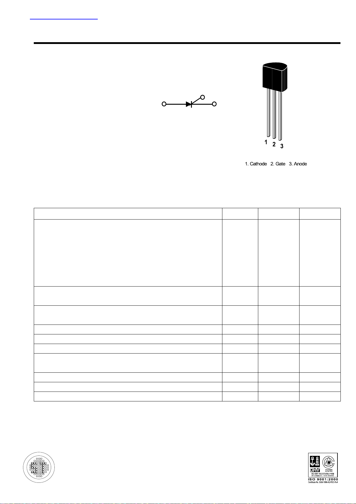
G
A
K
TO-92 Plastic Package
Weight approx. 0.18g
MAXIMUM RATINGS (TJ=25°C unless otherwise noted.)
Rating Symbol Value Unit
Peak Repetitive Forward and Reverse Blocking
Voltage, Note 1
=25 to 125°C, RGK=1KΩ)
(T
J
Forward Current RMS
(All Conduction Angles)
Peak Forward Surge Current, TA=25°C
(1/2 Cycle, Sine Wave, 60Hz)
MCR100-3
MCR100-4
MCR100-5
MCR100-6
MCR100-7
MCR100-8
100
V
DRM
and
V
RRM
200
300
400
Volts
500
600
0.8 Amps
I
T(RMS)
10 Amps
I
TSM
Circuit Fusing (t=8.3ms) I2t 0.415 A2s
Peak Gate Power - Forward, TA=25°C PGM 0.1 Watts
Average Gate Power - Forward, TA=25°C P
Peak Gate Current - Forward, TA=25°C
(300µs,120PPS)
Peak Gate Voltage - Reverse V
Operating Junction Temperature Range @ Rated V
RRM
and V
T
DRM
0.01 Watt
GF(AV)
1 Amp
I
GFM
5 Volts
GRM
-40 to +125 °C
J
Storage Temperature Range Ts -40 to +150 °C
Note 1. Ratings apply for zero or negative gate voltage; however, positive gate voltage shall not be applied
concurrent with negative potential on the anode.
GSP FORM A IS AVAILABLE
SEMTECH ELECTRONICS LTD.
®
( Wholly owned subsidiary of Honey Technology Ltd.)
Dated : 06/12/2003
MCR100-3 … MCR100-8
CHARACTERISTICS (TC=25°C, RGK=1KΩ unless otherwise noted.)
Characteristic Symbol Min Max Unit
Peak Forward or Reverse Blocking Current
(VAK=Rated V
Forward “On” Voltage
(ITM=1A Peak @TA=25°C)
Gate Trigger Current(Continuous dc),Note 1
(Anode Voltage=7Vdc,RL=100 Ohms)
Gate Trigger Voltage(Continuous dc)
(Anode Voltage=7Vdc,RL=100 Ohms)
(Anode Voltage=Rated V
Holding Current
(Anode Voltage=7Vdc,initiating current=20mA)
Note 1. RGK current is not included in measurement
DRM
or V
)
RRM
=100 Ohms)
DRM,RL
GSP FORM A IS AVAILABLE
I
DRM,IRRM
-
10
VTM - 1.7 Volts
- 200 µA
I
GT
-
V
GT
IH - 5 mA
0.8 Volts
µA
.
SEMTECH ELECTRONICS LTD.
®
( Wholly owned subsidiary of Honey Technology Ltd.)
Dated : 06/12/2003
MCR100-3 … MCR100-8
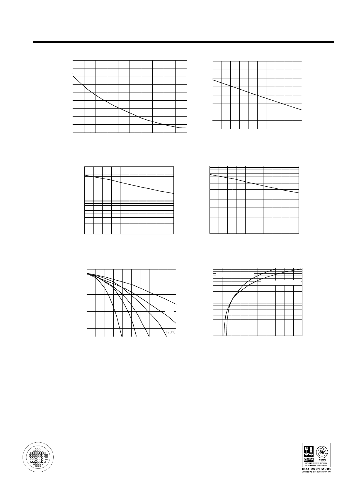
100
90
80
(µA)
70
60
50
40
30
20
Gate Trigger Current
10
-40
5
-10-25
20
T
, Junction Temperature (〜C)
J
Figure 1. Typical Gate Trigger Curent Versus
Junction Temperature
1000
(µA)
100
655035 9580
110
1.0
0.9
0.8
0.7
0.6
0.5
0.4
0.3
Gate Trigger Voltage (volts)
0.2
-25 -10-40
5
35
20 8050 65 11095
TJ, Junction Temperature (〜C)
Figure 2. Typical Gate Trigger Voltage
Versus Junction Temperature
1000
(µA)
100
Holding Current
10
-10-40 -25
T
, Junction Temperature (〜C)
J
520
35
8050 65 95 110
Figure 3. Typical Holding Curent Versus
Junction Temperature
120
110
100
90
C)
〜
80
70
60
50
, Maximum Allowable Case
C
T
Temperature (
40
0.1
00.2
T(RMS)
I
, RMS On-State Current (AMPS)
30〜C
60〜C
0.3
90〜C
0.4
Figure 5. Typical RMS Current Derating
DC
180〜C
0.5
Latching Current
-4010-10-25
5
J
T
, Junction Temperature (〜C)
503520 8065 110
95
Figure 4. Typical Latching Curent Versus
Junction Temperature
10
MAXIMUM @ TJ=25〜C
MAXIMUM @ TJ=110〜C
1
,Instantaneous On-State
T
Current (AMPS)
I
0.1
V
1.10.80.5
, Instantaneous On-State Voltage (volts)
T
2.01.71.4 2.92.62.3 3.53.2
Figure 6. Typical On-State Characteristics
SEMTECH ELECTRONICS LTD.
®
( Wholly owned subsidiary of Honey Technology Ltd.)
Dated : 06/12/2003
 Loading...