

Page 1
Wide bandwidth dual bipolar operational amplifier
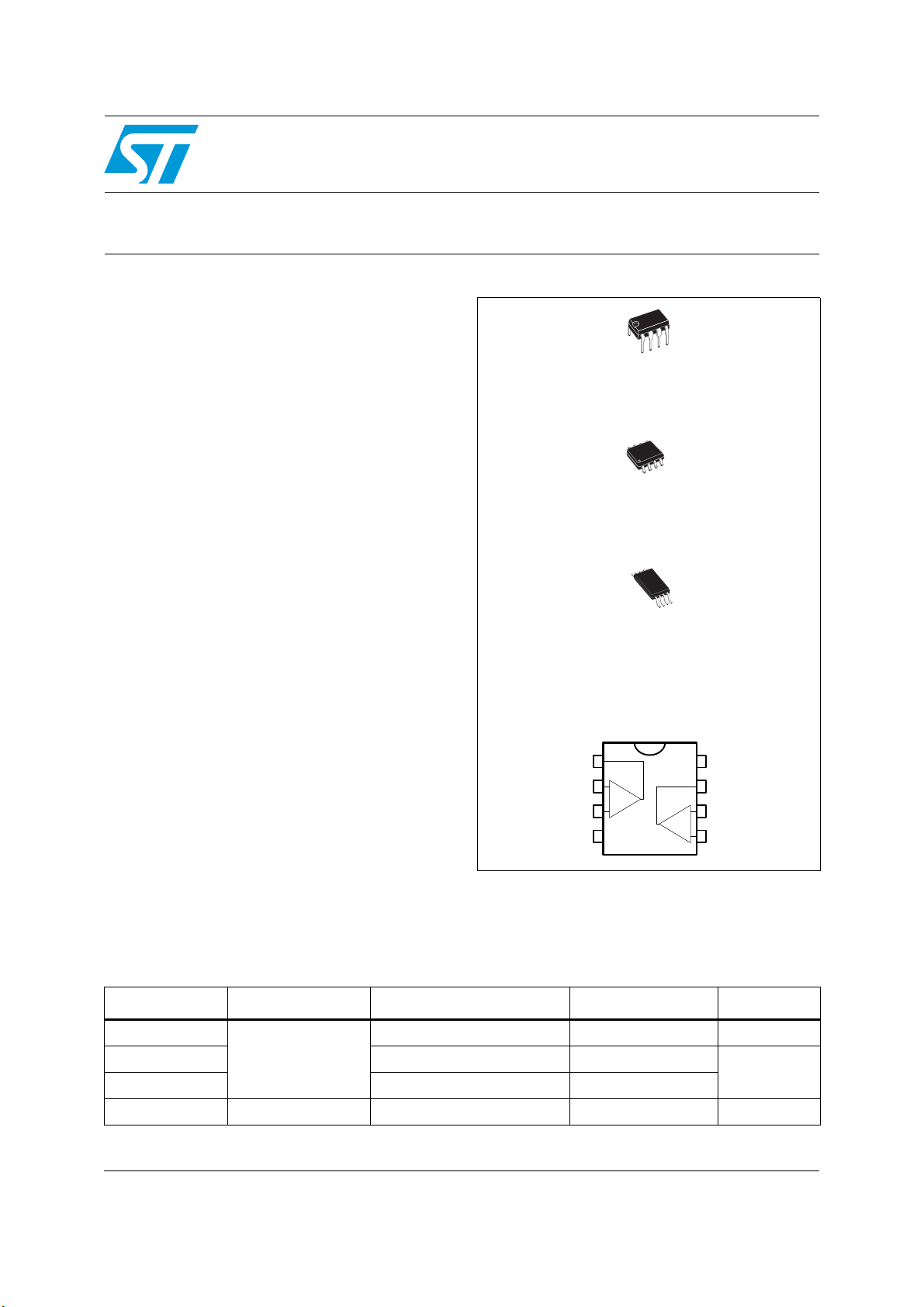
Pin connections (top view)
N
DIP8
(Plastic package)
D
SO-8
(Plastic micropackage)
P
TSSOP8
(Thin shrink small outline package)
Features
■ Internally compensated
■ Short-circuit protection
■ Gain and phase match between amplifier
■ Low power consumption
■ Pin-to-pin compatible with MC1458/LM358
■ Gain bandwidth (at 100 kHz): 5.5 MHz
Description
The MC4558 is a high performance monolithic
dual operational amplifier.
The circuit combines all of the outstanding
features of the MC1458, and in addition
possesses three times the unity gain bandwidth of
the industry standard.
MC4558
Datasheet − production data
Table 1. Device summary
Order codes Temperature range Package Packing Marking
MC4558CN
MC4558CD/CDT SO-8 Tube or tape & reel
MC4558CPT TSSOP8 Tape & reel
0 °C to +70 °C
MC4558ID/IDT -40 °C to +105 °C SO-8 Tube or tape & reel 4558I
April 2012 Doc ID 2181 Rev 3 1/11
This is information on a product in full production.
7
$$
0VUQVU
*OWFSUJOHJOQVU
/POJOWFSUJOHJOQVU
*OWFSUJOHJOQVU
/POJOWFSUJOHJOQVU
0VUQVU
7
$$
DIP8 Tube MC4558CN
4558C
www.st.com
11
Page 2
Absolute maximum ratings MC4558
1 Absolute maximum ratings
Table 2. Key parameters and their absolute maximum ratings
Symbol Parameter MC4558I MC4558C Unit
V
V
V
id
P
Supply voltage ±22 V
CC
(1)
Input voltage ±15 V
i
(2)
Differential input voltage ±30 V
Power dissipation 680 mW
tot
Output short-circuit duration Infinite
T
oper
Operating free-air temperature range -40 to +105 0 to +70 °C
Thermal resistance junction-to-ambient:
R
thja
ESD
SO-8
TSSOP8
DIP8
HBM: Human body model
(4)
(3)
125
120
85
500
200
°C/W
CDM: Charged device model 1500
1. Input voltage is with respect to the midpoint between Vcc+ and Vcc-. Its value must never exceed 15 V or
the magnitude of Vcc, whichever is less.
2. Differential voltages are the non-inverting input terminal with respect to the inverting input terminal.
3. Human body model, 100 pF discharged through a 1.5 kΩ resistor into pin of device.
4. Machine model ESD, a 200 pF cap is charged to the specified voltage, then discharged directly into the IC
with no external series resistor (internal resistor < 5 Ω), into pin of device.
VMM: Machine model
Table 3. Operating conditions
Symbol Parameter Min. Max. Unit
V
2/11 Doc ID 2181 Rev 3
Supply voltage ±2 ±20 V
CC
Page 3
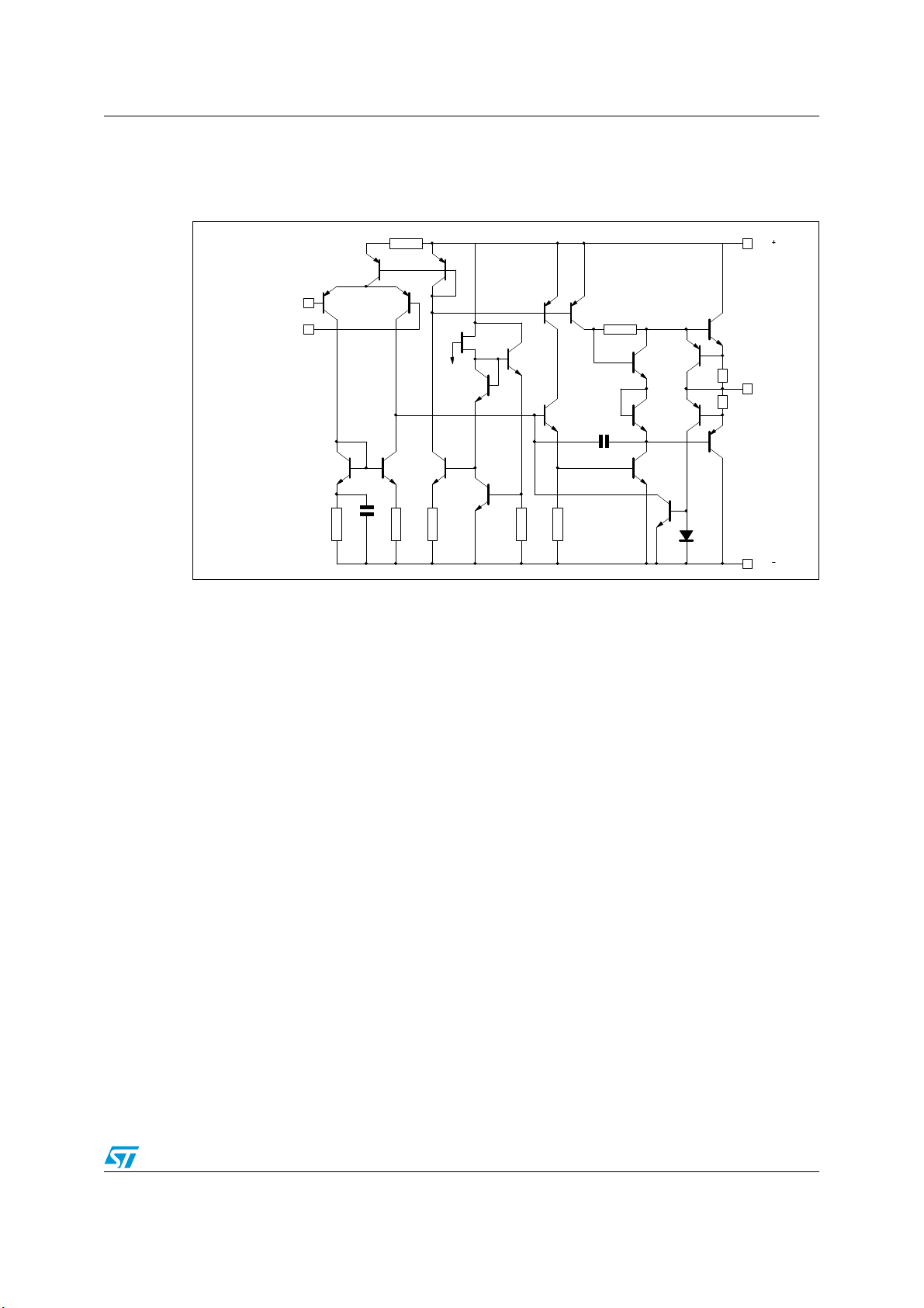
MC4558 Typical application schematic
2 Typical application schematic
Figure 1. Schematic diagram (1/2MC4558)
L
8
7
$$
*OWFSUJOHJOQVU
/POJOWFSUJOHJOQVU
L
8
8
0VUQVU
8
Q'
Q'
L8
8
8
L
8
L
8
7
$$
Doc ID 2181 Rev 3 3/11
Page 4
Electrical characteristics MC4558
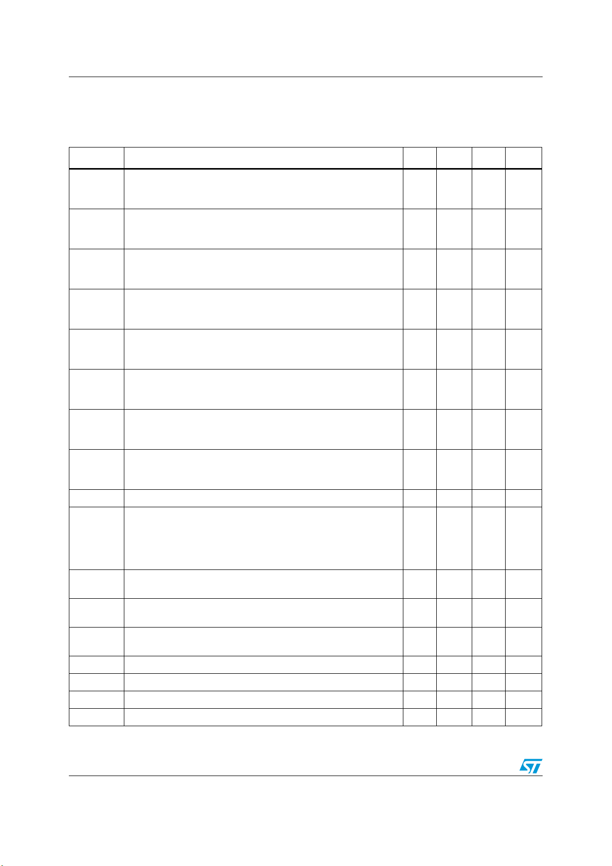
3 Electrical characteristics
Table 4. Electrical characteristics for VCC = ±15 V, T
= 25 °C (unless otherwise specified)
amb
Symbol Parameter Min. Typ. Max. Unit
Input offset voltage (Rs ≤ 10kΩ)
V
io
T
T
amb
min
= +25°C
. ≤ T
amb
≤ T
156mV
max.
Input offset current
I
io
T
T
amb
min
= +25°C
. ≤ T
amb
≤ T
max.
20 100
200
Input bias current
I
ib
T
T
amb
min
= +25°C
. ≤ T
amb
≤ T
max.
50 400
500
Large signal voltage gain (RL = 2kΩ, Vo = ±10V)
A
vd
SVR
T
= +25°C
amb
. ≤ T
T
min
amb
≤ T
max.
Supply voltage rejection ratio (R
= +25°C
T
amb
T
. ≤ T
amb
≤ T
max.
min
≤ 10kΩ)
s
50
25
77
77
200 V/mV
90 dB
Supply current, all amplifiers, no load
I
CC
T
T
amb
min
= +25°C
. ≤ T
amb
≤ T
max.
2.3 4.5
6
Input common mode voltage range
V
icm
CMR
I
os
= +25°C
T
amb
T
. ≤ T
amb
≤ T
max.
min
Common-mode rejection ratio (R
= +25°C
T
amb
T
. ≤ T
amb
≤ T
max.
min
≤ 10kΩ)
s
±12
±12
70
70
90 dB
Output short-circuit current 10 20 40 mA
Output voltage swing
V
o
SR
t
r
KOV
R
C
R
o
T
= +25°C RL = 10kΩ
amb
= 2kΩ
R
L
. ≤ T
T
min
R
L
= 2kΩ
amb
≤ T
max. RL
= 10kΩ
±12
±10
±12
±10
Slew rate
= ±10, RL = 2kΩ, CL = 100pF, T
V
i
= 25°C, unity gain 1.5 2.2
amb
Rise time
Vi = ±20mV, RL = 2kΩ, CL = 100pF, T
= 25°C, unity gain 0.3
amb
Overshoot
V
= ±20mV, RL = 2kΩ, CL = 100pF, T
i
Input resistance 0.3 2 MΩ
i
Input capacitance 1.4 pF
i
= 25°C, unity gain 15
amb
Output resistance 75 Ω
±14
±13 V
B Unity gain bandwidth 2.8 MHz
nA
nA
mA
V
V/µs
µs
%
4/11 Doc ID 2181 Rev 3
Page 5

MC4558 Electrical characteristics
nV
Hz
------------
Table 4. Electrical characteristics for VCC = ±15 V, T
= 25 °C (unless otherwise specified)
amb
Symbol Parameter Min. Typ. Max. Unit
GBP
THD
e
VO1/V
n
Gain bandwidth product
= 10mV, RL = 2kΩ, CL = 100pF, f = 100kHz, T
V
i
= 25°C 5.5
amb
Total harmonic distortion
f = 1kHz, A
= 20dB, RL = 2kΩ, Vo = 2Vpp, CL = 100pF, T
v
= 25°C 0.008
amb
Equivalent input noise voltage (RS = 100Ω, f = 1kHz) 12
Channel separation 120 dB
O2
MHz
%
Doc ID 2181 Rev 3 5/11
Page 6

Electrical characteristics MC4558
04$*--04$01&
04$*--04$01&
7
*
$
-
3
-
Figure 2. Transient response test circuit Figure 3. Positive output voltage swing vs.
load resistance
Figure 4. Open loop frequency response Figure 5. Negative output voltage swing vs.
load resistance
Figure 6. Phase margin vs. frequency Figure 7. Power bandwidth
6/11 Doc ID 2181 Rev 3
Page 7

MC4558 Package mechanical data
DIM.
mm. inch
MIN. TYP MAX. MIN. TYP. MAX.
A 3.3 0.130
a1 0.7 0.028
B 1.39 1.65 0.055 0.065
B1 0.91 1.04 0.036 0.041
b 0.5 0.020
b1 0.38 0.5 0.015 0.020
D 9.8 0.386
E 8.8 0.346
e 2.54 0.100
e3 7.62 0.300
e4 7.62 0.300
F 7.1 0.280
I 4.8 0.189
L 3.3 0.130
Z 0.44 1.6 0.017 0.063
Plastic DIP-8 MECHANICAL DATA
P001F
4 Package mechanical data
In order to meet environmental requirements, ST offers these devices in different grades of
ECOPACK
specifications, grade definitions and product status are available at: www.st.com.
ECOPACK
®
packages, depending on their level of environmental compliance. ECOPACK®
®
is an ST trademark.
Figure 8. DIP8 package
Doc ID 2181 Rev 3 7/11
Page 8

Package mechanical data MC4558
DIM.
mm. inch
MIN. TYP MAX. MIN. TYP. MAX.
A 1.35 1.75 0.053 0.069
A1 0.10 0.25 0.04 0.010
A2 1.10 1.65 0.043 0.065
B 0.33 0.51 0.013 0.020
C 0.19 0.25 0.007 0.010
D 4.80 5.00 0.189 0.197
E 3.80 4.00 0.150 0.157
e 1.27 0.050
H 5.80 6.20 0.228 0.244
h 0.25 0.50 0.010 0.020
L 0.40 1.27 0.016 0.050
k ˚ (max.)
ddd 0.1 0.04
SO-8 MECHANICAL DATA
0016023/C
8
Figure 9. SO-8 package
8/11 Doc ID 2181 Rev 3
Page 9

MC4558 Package mechanical data
DIM.
mm. inch
MIN. TYP MAX. MIN. TYP. MAX.
A 1.2 0.047
A1 0.05 0.15 0.002 0.006
A2 0.80 1.00 1.05 0.031 0.039 0.041
b 0.19 0.30 0.007 0.012
c 0.09 0.20 0.004 0.008
D 2.90 3.00 3.10 0.114 0.118 0.122
E 6.20 6.40 6.60 0.244 0.252 0.260
E1 4.30 4.40 4.50 0.169 0.173 0.177
e 0.65 0.0256
K0˚ 8˚0˚ 8˚
L 0.45 0.60 0.75 0.018 0.024 0.030
L1 1 0.039
TSSOP8 MECHANICAL DATA
0079397/D
Figure 10. TSSOP8 package
Doc ID 2181 Rev 3 9/11
Page 10

Revision history MC4558
5 Revision history
Table 5. Document revision history
Date Revision Changes
Oct-2001 1 Initial release.
The following changes were made in this revision:
– Table 3.: Operating conditions on page 2 updated with Vcc min.
Oct-2005 2
13-Apr-2012 3
and max.
– Addition of supplementary data in Table 2.: Key parameters and
their absolute maximum ratings on page 2
Minor grammatical and formatting changes throughout.
– ESD MM changed from 500 V to 200 V in Table 2: Key parameters
and their absolute maximum ratings
– Order codes MC4558IN and MC4558IPT removed from Table 1.:
Device summary
– Minor text and formatting changes throughout.
10/11 Doc ID 2181 Rev 3
Page 11

MC4558
Please Read Carefully:
Information in this document is provided solely in connection with ST products. STMicroelectronics NV and its subsidiaries (“ST”) reserve the
right to make changes, corrections, modifications or improvements, to this document, and the products and services described herein at any
time, without notice.
All ST products are sold pursuant to ST’s terms and conditions of sale.
Purchasers are solely responsible for the choice, selection and use of the ST products and services described herein, and ST assumes no
liability whatsoever relating to the choice, selection or use of the ST products and services described herein.
No license, express or implied, by estoppel or otherwise, to any intellectual property rights is granted under this document. If any part of this
document refers to any third party products or services it shall not be deemed a license grant by ST for the use of such third party products
or services, or any intellectual property contained therein or considered as a warranty covering the use in any manner whatsoever of such
third party products or services or any intellectual property contained therein.
UNLESS OTHERWISE SET FORTH IN ST’S TERMS AND CONDITIONS OF SALE ST DISCLAIMS ANY EXPRESS OR IMPLIED
WARRANTY WITH RESPECT TO THE USE AND/OR SALE OF ST PRODUCTS INCLUDING WITHOUT LIMITATION IMPLIED
WARRANTIES OF MERCHANTABILITY, FITNESS FOR A PARTICULAR PURPOSE (AND THEIR EQUIVALENTS UNDER THE LAWS
OF ANY JURISDICTION), OR INFRINGEMENT OF ANY PATENT, COPYRIGHT OR OTHER INTELLECTUAL PROPERTY RIGHT.
UNLESS EXPRESSLY APPROVED IN WRITING BY TWO AUTHORIZED ST REPRESENTATIVES, ST PRODUCTS ARE NOT
RECOMMENDED, AUTHORIZED OR WARRANTED FOR USE IN MILITARY, AIR CRAFT, SPACE, LIFE SAVING, OR LIFE SUSTAINING
APPLICATIONS, NOR IN PRODUCTS OR SYSTEMS WHERE FAILURE OR MALFUNCTION MAY RESULT IN PERSONAL INJURY,
DEATH, OR SEVERE PROPERTY OR ENVIRONMENTAL DAMAGE. ST PRODUCTS WHICH ARE NOT SPECIFIED AS "AUTOMOTIVE
GRADE" MAY ONLY BE USED IN AUTOMOTIVE APPLICATIONS AT USER’S OWN RISK.
Resale of ST products with provisions different from the statements and/or technical features set forth in this document shall immediately void
any warranty granted by ST for the ST product or service described herein and shall not create or extend in any manner whatsoever, any
liability of ST.
ST and the ST logo are trademarks or registered trademarks of ST in various countries.
Information in this document supersedes and replaces all information previously supplied.
The ST logo is a registered trademark of STMicroelectronics. All other names are the property of their respective owners.
© 2012 STMicroelectronics - All rights reserved
STMicroelectronics group of companies
Australia - Belgium - Brazil - Canada - China - Czech Republic - Finland - France - Germany - Hong Kong - India - Israel - Italy - Japan -
Malaysia - Malta - Morocco - Philippines - Singapore - Spain - Sweden - Switzerland - United Kingdom - United States of America
www.st.com
Doc ID 2181 Rev 3 11/11
 Loading...