

DC/DC CONVERTER CONTROL CIRCUITS
■ OUTPUT SWITCH CURRENT IN EXCESS
OF 1.5A
■ 2% REFERENCE ACCURACY
■ LOW QUIESCENT CURRENT: 2.5mA (TYP.)
■ OPERATINGFROM3VTO40V
■ FREQUENCY OPERATION TO 100KHz
■ ACTIVE CURRENT LIMITING
MC34063A
MC34063E
DESCRIPTION
The MC34063A/E series is a monolithic control
circuit delivering the main functions for DC/DC
voltage converting.
The device contains an internal temperature
compensated reference, comparator, duty cycle
controlled oscillator with an active current limit
circuit, driver and high current output switch.
Output v oltage is adjustable through two external
resistors with a 2% reference accuracy.
Employing a minimum number of ex ternal
components the MC34063A /E de vice s series is
designed for Step-Down, Step-Up and
Voltage-Inverting applications.
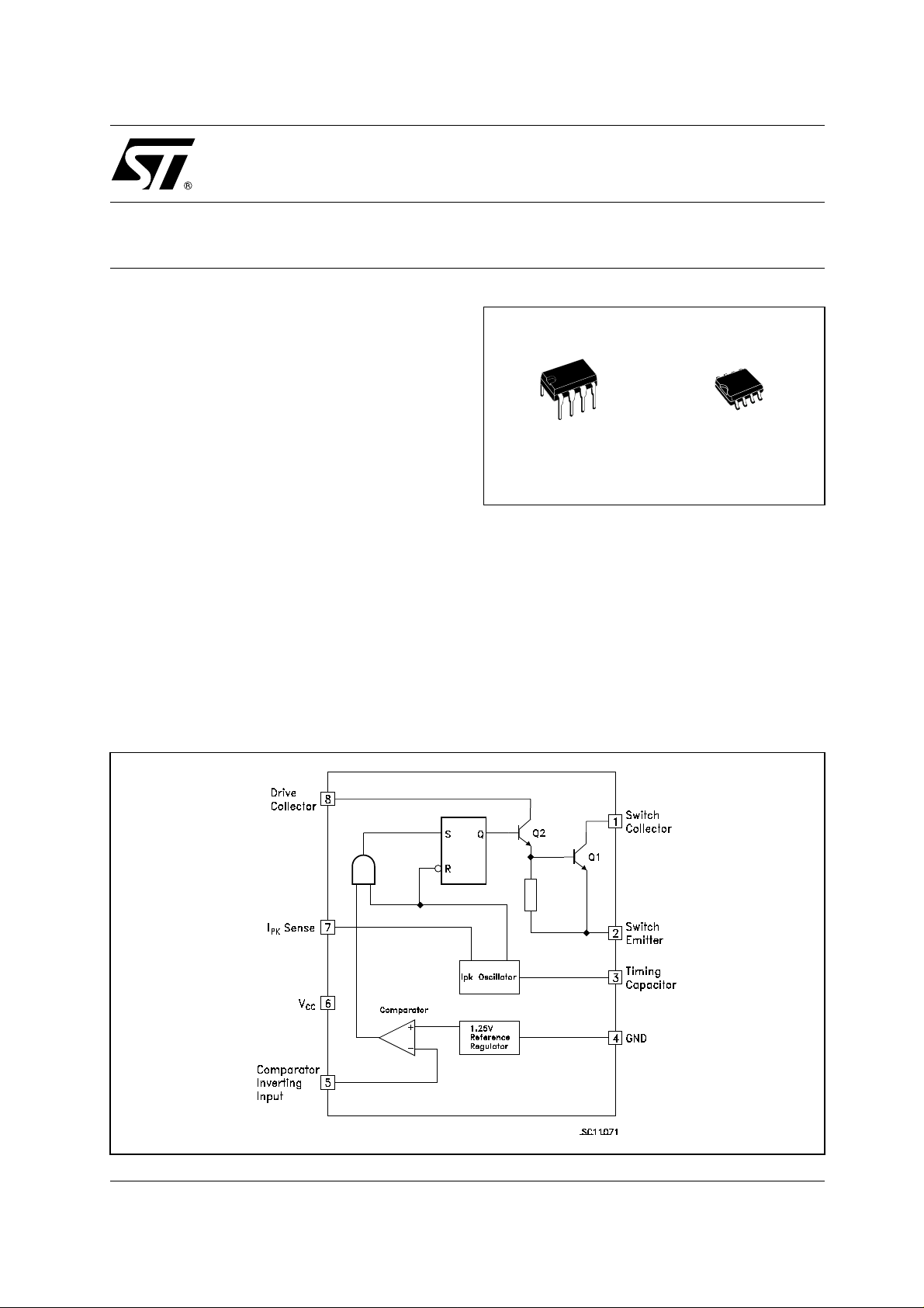
BLOCK DIAGRAM
DIP-8 SO-8
1/16March 2004
MC34063A/E
ABSOLUTE MAXIMUM RATINGS
Symbol Parameter Value Unit
V
V
V
SWC
V
SWE
V
V
I
DC
I
SW
P
TOT
T
T
STG
T
Absolute Maximum Ratings are those values beyond which damage to the device may occur. Functional operation under these condition is
not implied.
Power Supply Voltage
CC
Comparator Input Voltage Range
IR
Switch Collector Voltage
Switch Emitter Voltage (V
Switch Collector to Emitter Voltage
CE
Driver Collector Voltage
DC
SWC
=40V)
Driver Collector Current
Switch Current
Power Dissipation at TA= 25°C for DIP-8 1.25
for SO-8 0.625
Operating Junction Temperature
J
Storage Temperature Range
Operating Ambient Temperature Range for AC and EC SERIES 0 to 70
OP
for EB SERIES -40 to 125
50 V
-0.3 to 40 V
40 V
40 V
40 V
40 V
100 mA
1.5 A
W
150 °C
-40 to 150 °C
°Cfor AB SERIES -40 to 85
THERMAL DATA
Symbol Parameter DIP-8 SO-8 Unit
R
thj-amb
R
thj-case
(*) This value depends from thermal design of PCB on which the device is mounted.
Thermal Resistance Junction-ambient (*)
Thermal Resistance Junction-case
100 160 °C/W
42 20 °C/W
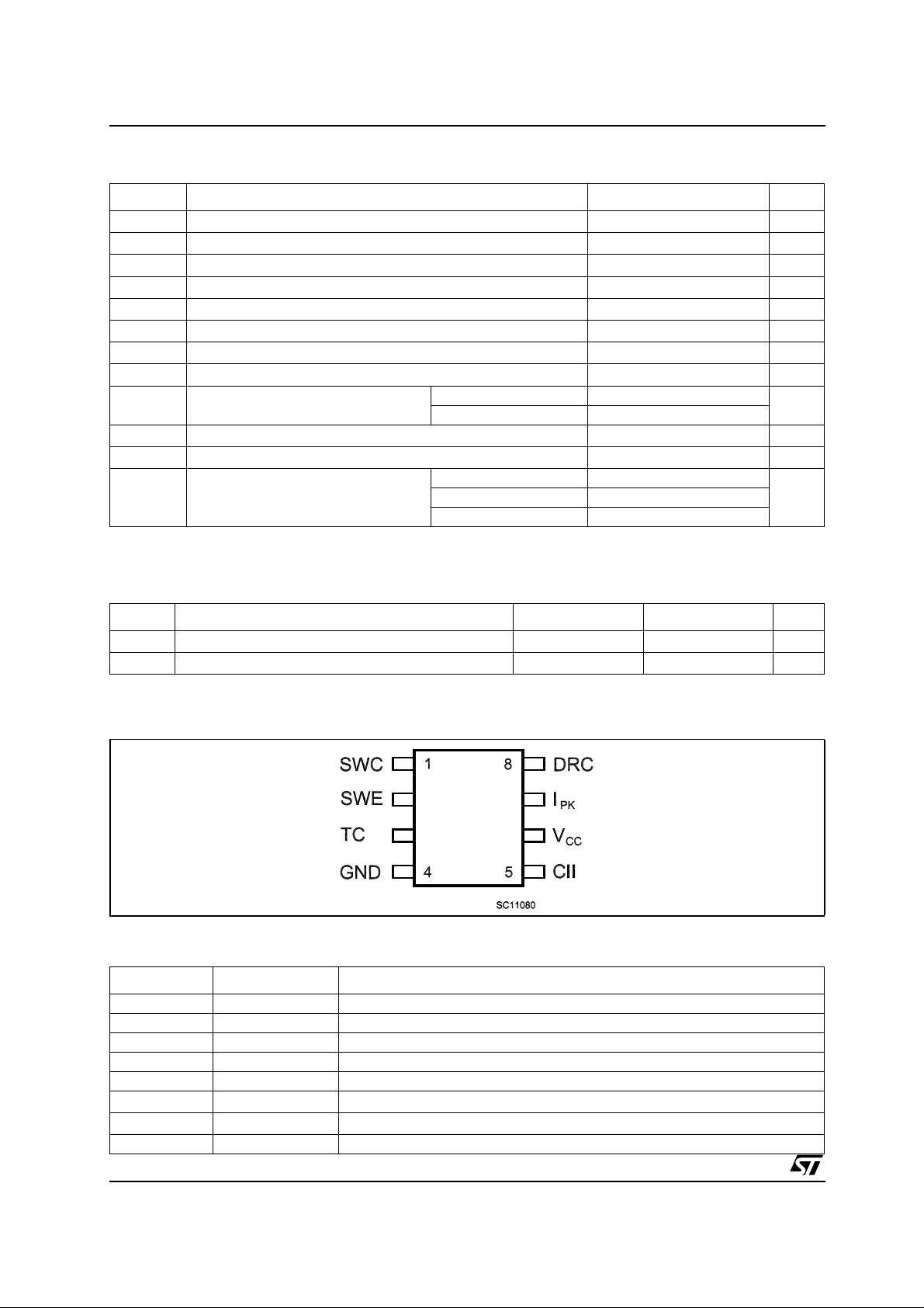
CONNECTION DIAGRAM (top view)
PIN DESCRIPTION
Pin N° Symbol Name and Function
1 SWC Switch Collector
2 SWE Switch Emitter
3 TC Timing Capacitor
4 GND Ground
5 CII Comparator Inverting Input
2/16
6V
7I
CC
PK
8 DRC Voltage Driver Collector
Voltage Supply
IPKSense
ORDERING CODES
TYPE DIP-8 SO-8 SO-8 (TAPE & REEL)
MC34063AB MC34063ABN MC34063ABD MC34063ABD-TR
MC34063AC MC34063ACN MC34063ACD MC34063ACD-TR
MC34063EB MC34063EBN MC34063EBD MC34063EBD-TR
MC34063EC MC34063ECN MC34063ECD MC34063ECD-TR
(*) The "A" version is not recommended for new designs.
MC34063A/E
ELECTRICAL CHARACTERISTICS (Refer to the t es t circuits, VCC=5V,TA=T
LOW
to T
HIGH
, unless
otherwise specified, see note 2)
OSCILLATOR
Symbol Parameter Test Conditions Min. Typ. Max. Unit
f
OSC
I
CHG
I
DISCHG
I
DISCHG
I
CHG
V
IPK(sense)
Frequency V
=0V CT=1nF TA=25°C243342KHz
PIN5
Charge Current VCC= 5 to 40V TA=25°C 243342µA
Discharge Current VCC= 5 to 40V TA= 25°C 140 200 260 µA
/
Discharge to Charge Current
Ratio
Current Limit Sense Voltage I
PIN 7 = V
CHG=IDISCHG
CC
TA= 25°C 5.2 6.2 7.5 µA
TA= 25°C 250 300 350 mV
OUTPUT S WITCH
Symbol Parameter Test Conditions Min. Typ. Max. Unit
V
CE(sat)
V
CE(sat)
Saturation Voltage, Darlington
ISW= 1 A PIN 7, 8 connected 1 1.3 V
Connection
Saturation Voltage ISW=1A R
=82Ω to V
PIN8
CC
0.45 0.7 V
Forced β ~20
h
I
C(off)
DC Current Gain ISW=1A VCE=5V TA= 25°C 50 120
FE
Collector Off-State Current VCE=40V 0.01 100 µA
COMPARATOR
Symbol Parameter Test Conditions Min. Typ. Max. Unit
V
Reg
I
Threshold Voltage TA= 25°C 1.225 1.25 1.275 V
TH
T
A=TLOW
Threshold Voltage Line
line
Regulation
Input Bias Current VIN= 0 V -5 -400 nA
IB
VCC=3to40V 1 5 mV
to T
HIGH
1.21 1.29
3/16
MC34063A/E
TOTAL DEVICE
Symbol Parameter Test Conditions Min. Typ. Max. Unit
I
V
START-UP
NOTES:
1) Maximum package power dissipation limit must beobserved.
2) T
LOW
3) If Darlington configuration is not used, care must be taken to avoid deep saturation of output switch. The resulting switch-off time may be
adversely affected. In a Darlington configuration the following output driver condition is suggested:
Forced
* Current lessdue to a built in 1KΩ anti leakage resistor.
4) Start-up Voltage is the minimum PowerSupply Voltag e at which the internal oscillator b egins to work.
TYPICAL P E RFORMAN CE CHARACTE RISTICS
Supply Current VCC=5to40V
CC
Start-Up Voltage (Note 4) TA=25°C
=0°C,T
β of output current switch = I
= 70°C (AC and EC series); T
HIGH
COUTPUT
/(I
CDRIVER
C
=1nF
T
PIN 7 = V
V
PIN5>VTH
CC
PIN 2 = GND
Remaining pins open
C
=1µF,PIN5=0
T
=-40°C,T
LOW
-1mA*)≥ 10
= 85°C (AB series); T
HIGH
for MC34063A 2.5 4 mA
1.5 4for MC34063E
for MC34063A 2.1 V
for MC34063E 1.5
LOW
= -40°C, T
= 125°C (EB series).
HIGH
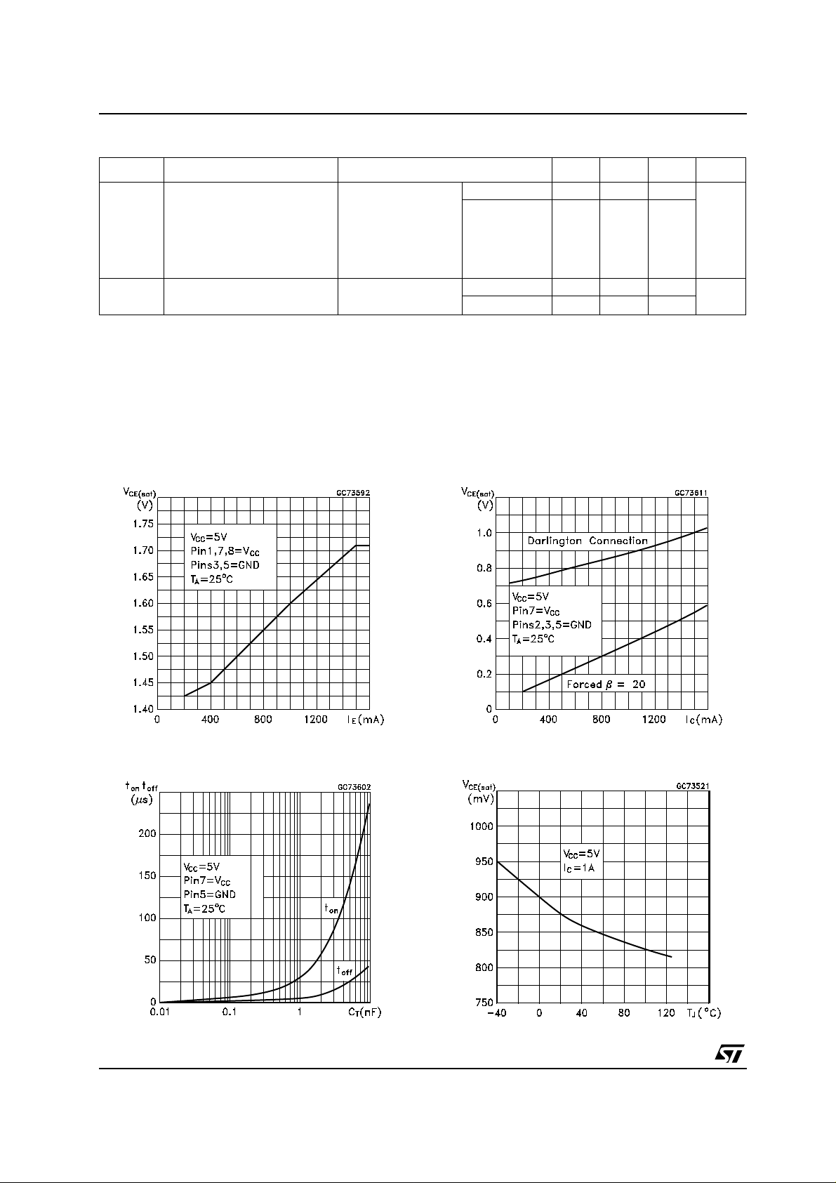
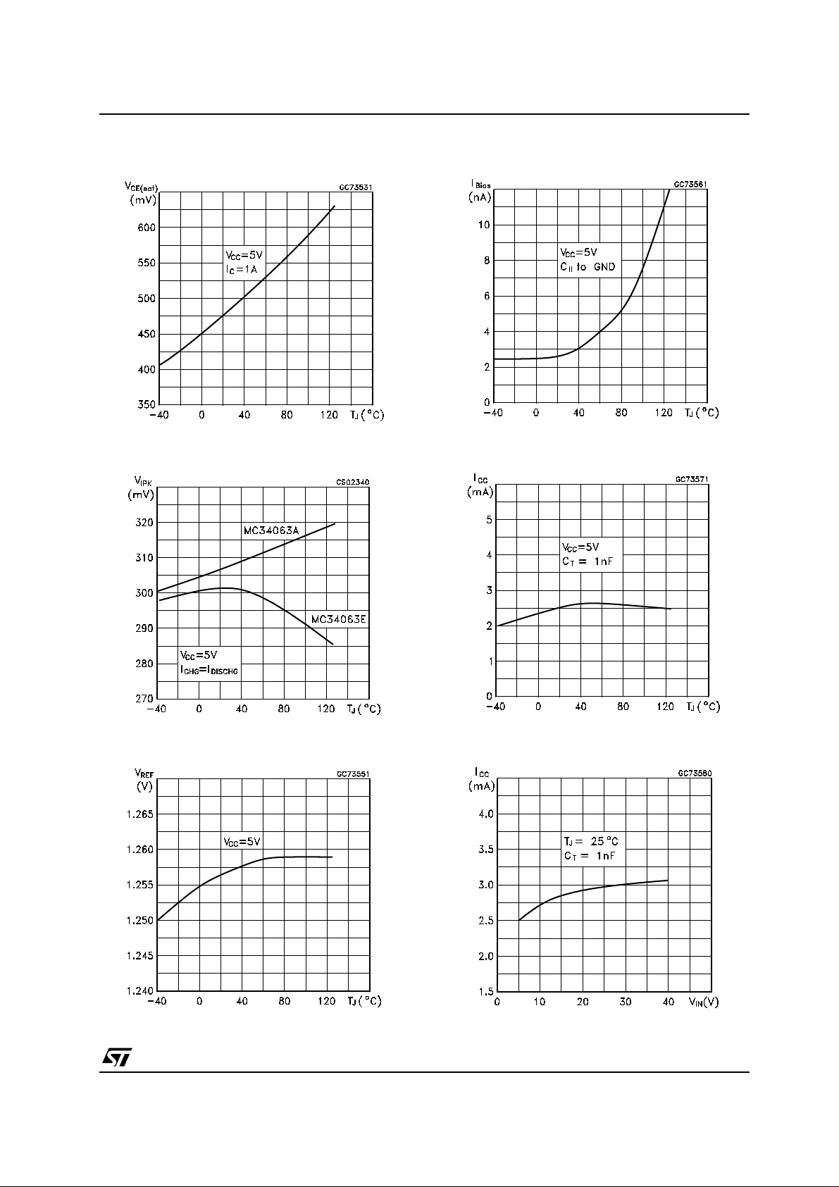
Figure1 : Emitter Follower Configuration Output
Saturation Voltage vs Emitter Current
Figure2 : Output SwitchON-OFF Time vs
Oscillator Timing Capacitor
Figure3 : Common Emitter Configuration Output
Switch Saturation Voltage vs Collector Current
Figure4 : Darlington Configuration Collector
Emitter Saturation Voltage (V
CEsat)
vs Temperat.
4/16
MC34063A/E
Figure5 : Power Collector E mi tter Saturation
Voltage (V
Figure6 : Current Limit Sense Voltage (V
vs Temperature
CEsat)
IPK
Temperature
)vs
Figure8 : Bias Current vs Temperat ure
Figure9 : Supply Current vs Temperature
Figure7 : Reference V oltage v s Temp eratu re
Figure10 : Supply Current vs Input Voltage
5/16

MC34063A/E
TYPICAL APP LICATION CIRCUIT
Step-UP Converter
Printed Demoboard
Test Condition (V
Test Conditions Value (Typ.) Unit
Line Regulation V
Load Regulation V
Output Ripple V
Efficiency V
OUT
= 28V)
PIN 1 = V
PIN 2 = GND
OUT
PIN 3 = GND
PIN 4 = V
=8to16V, IO= 175 mA 30 mV
IN
=12V, IO=75to175mA 10 mV
IN
=12V, IO= 175 mA 300 mV
IN
=12V, IO= 175 mA 89 %
IN
IN
6/16

Step-Down Converter
MC34063A/E
Printed Demoboard
Test Condition (V
Test Conditions Value (Typ.) Unit
Line Regulation V
Load Regulation V
Output Ripple V
Efficiency V
I
SC
OUT
=5V)
PIN 1 = V
PIN 2 = GND
OUT
PIN 3 = GND
PIN 4 = V
=15to25V, IO= 500 mA 5 mV
IN
=25V, IO=50to500mA 30 mV
IN
=25V, IO= 500 mA 100 mV
IN
=25V, IO= 500 mA 80 %
IN
VIN=25V, R
=0.1Ω 1.2 A
LOAD
IN
7/16

MC34063A/E
Voltage Inverting Converter
Printed Demoboard
Test Condition (V
Test Conditions Value (Typ.) Unit
Line Regulation V
Load Regulation V
Output Ripple V
Efficiency V
I
SC
OUT
= - 12V)
PIN 1 = V
PIN 2 = GND
OUT
PIN 3 = GND
PIN 4 = V
= 4.5 to 6 V, IO= 100 mA 15 mV
IN
=5V, IO=10to100mA 20 mV
IN
=5V, IO= 100 mA 230 mV
IN
=5V, IO= 100 mA 58 %
IN
VIN=5V, R
=0.1Ω 0.9 A
LOAD
IN
8/16

Calculation
)
MC34063A/E
Parameter
t
on/toff
(ton+t
C
I
PK(switch)
R
C
L
NOTES:
V
SAT
V
F
THE FOLLOWING POWER SUPPLY CHARACTERISTICS MUST BE CHOSEN:
V
IN
V
OUT
I
OUT
f
MIN
V
RIPPLE
series resistance and board layout. The ripple voltage should be kept to a low value since it will directly affect the line and load regulation.
)max 1/f
off
T 4.5x10
SC
O
(min)
= Saturation voltage of the output switch
= Forward voltage drop of the output rectifier
= Nominalinputvoltage
= Desired output voltage, |V
= Desired output current
= Minimum desired output switching frequency at the selected values of VINand I
= Desired peak to peak output ripple voltage. In practice, the calculated capacitor value will and to be increased due to its equivalent
Step-Up
(Discontinuous mode)
V
OUTVFVIN min()
------------------------------------------------------- -
V
2I
out(max)
V
IN min()Vsat
-------------------------------------- -
I
PK switch()
OUT
–+
–
IN m in()Vsat
min
-5
t
on
[(ton/t
off
0.3/I
PK(switch)
I
outton
-------------------------------
V
ripple p p–()
–
×
| = 1.25(1+R2/R1)
)+1] 2I
t
on min()
V
--------------------------------------------------------
Step-Down
(Continuous mode)
V
+
OUTVF
----------------------------------------------------------- -
V
IN m in()Vsat
– V
IN min()Vsat
4.5x10⁻⁵t
0.3/I
I
PK switch()tontoff
------------------------------------------------------
8V
– V
I
PK swit ch()
–
1/f
min
on
out(max)
PK(switch)
+()
ripple p p–()
–
out
O
OUT
t
×
on min(
Voltage Inverting
(Discontinuous mode)
V
+
OUTVF
------------------------------–
V
INVsat
1/f
min
4.5x10⁻⁵t
2I
out(max)
0.3/I
-------------------------------
V
V
IN min()Vsat
-------------------------------------- -
I
PK switch()
on
[(ton/t
)+1]
off
PK(switch)
I
outton
ripple p p–()
–
t
×
on min()
Step-Up With External NP N Switch
9/16

MC34063A/E
Step-Down With External NP N Switch
Step-Down With External P N P Switch
10/16

Voltage Inverting With External NPN Switch
MC34063A/E
Voltage Inverting With External PNP Saturated Switch
11/16

MC34063A/E
Dual Output Voltage
Higher Output Power, Higher Input Voltage
12/16

Plastic DIP-8 MECHANICAL DATA
MC34063A/E
DIM.
MIN. TYP MAX. MIN. TYP. MAX.
A 3.3 0.130
a1 0.7 0.028
B 1.39 1.65 0.055 0.065
B1 0.91 1.04 0.036 0.041
b 0.5 0.020
b1 0.38 0.5 0.015 0.020
D 9.8 0.386
E 8.8 0.346
e 2.54 0.100
e3 7.62 0.300
e4 7.62 0.300
F 7.1 0.280
I 4.8 0.189
L 3.3 0.130
Z 0.44 1.6 0.017 0.063
mm. inch
P001F
13/16

MC34063A/E
SO-8 MECHANICAL DATA
DIM.
A 1.35 1.75 0.053 0.069
A1 0.10 0.25 0.04 0.010
A2 1.10 1.65 0.043 0.065
B 0.33 0.51 0.013 0.020
C 0.19 0.25 0.007 0.010
D 4.80 5.00 0.189 0.197
E 3.80 4.00 0.150 0.157
e 1.27 0.050
H 5.80 6.20 0.228 0.244
h 0.25 0.50 0.010 0.020
L 0.40 1.27 0.016 0.050
k ˚ (max.)
ddd 0.1 0.04
MIN. TYP MAX. MIN. TYP. MAX.
mm. inch
8
14/16
0016023/C

MC34063A/E
Tape & Reel SO-8 MECHANICAL DATA
mm. inch
DIM.
MIN. TYP MAX. MIN. TYP. MAX.
A 330 12.992
C 12.8 13.2 0.504 0.519
D 20.2 0.795
N 60 2.362
T 22.4 0.882
Ao 8.1 8.5 0.319 0.335
Bo 5.5 5.9 0.216 0.232
Ko 2.1 2.3 0.082 0.090
Po 3.9 4.1 0.153 0.161
P 7.9 8.1 0.311 0.319
15/16

MC34063A/E
Information furnished is believed to be accurate and reliable. However, STMicroelectronics assumes no responsibility for the
consequences of use of such inform ation nor fo r an y infring ement of p atents or o ther rights of third p arties which may r esult f rom
its use. No license is granted by implication or otherwise under any patent or patent rights of STMicroelectronics. Specifications
mentioned in this publication are subject to change without notice. This publication supersedes and replaces all information
previously supplied. STMicroelectronics products are not authorized for use as critical components in life support devices or
systems without express written approval of STMicroelectronics.
Australia - Belgium - Brazil - Canada - China - Czech Republic - Finland - France - Germany - Hong Kong - India - Israel - Italy - Japan -
Malaysia - Malta - Morocco - Singapore - Spain - Sweden - Switzerland - United Kingdom - United States.
The ST logo is a registered trademark of STMicroelectronics
All other names are the property of their respective owners
© 2004 STMicroelectronics - All Rights Reserved
STMicroelectronics GROUP OF COMPANIES
http://www.st.com
16/16
 Loading...