

ST MC3303, MC3403, MC3503 User Manual

Inverting Input 2
Non-inverting Input 2
Non-inverting Input 1
CC
V
-
CC
V
1
2
3
4
8
5
6
7
9
10
11
12
13
14
+
Output 3
Output 4
Non-inverting Input 4
Inverting Input 4
Non-inverting Input 3
Inverting Input 3
-
+
+
-
+
-
+
Output 1
Inverting Input 1
Output 2
MC3303
MC3403 - MC3503
LOW POWER
QUAD BIPOLAR OPERATIONAL AMPLIFIERS
■ SHORT-CIRCUIT PROTECTED OUTPUTS
■ CLASS AB OUTPUT STAGE FOR MINIMAL
CROSSOVER DISTORTION
■ SINGLE SUPPLY OPER ATION: +3V TO +36V
■ DUAL SUPPLIES: ±15V TO ±18V
■ LOW INPUT BIAS CURRENT: 500nA MAX
■ INTERNALLY COMPENSATED
■ SIMILAR PERFORMANCE TO POPULAR
UA741
DESCRIPTION
The MC3403 is a low-cos t, quad operational amplifier with true differential i nputs. The devic e has
electrical characteristics similar to the popular
UA741. However the MC3403, has several distinct advantages over standa rd operat iona l am plifiers types in single supply applications. The quad
amplifier can operate at supply voltage as low as 3
Volts or as high as 36 volts with quiescent currents
about one third of those associated with the
UA741 (on a per amplifier basis). The common-mode input range includes the negat ive sup ply, thereby eliminating the neces sity for external
biasing components in many applications.
N
DIP14
(Plastic Package)
(Plastic Micropackage)
P
TSSOP14
(Thin Shrink Small Outline Package)
PIN CONNECTIONS (top view)
D
SO14
ORDER CODE
Part
Number
Temperature
Range
MC3303 -40°C, +105°C
MC3403 0°C, +70°C
MC3503 -55°C, +125°C
Example : MC3403N
N = Dual in Line Package (DIP)
D = Small Outline Package (SO) - also available in Tape & Reel (DT)
P = Thin Shrink Small Outline Package (TSSOP) - only available
in Tape & Reel (PT)
November 2001
Package
NDP
•••
•••
•••
1/10
MC3303 - MC3403 - MC3503
V
CC
V
CC
+3V to +30V
1.5V to 18V
1.5V to 18V
V
CC
V
CC
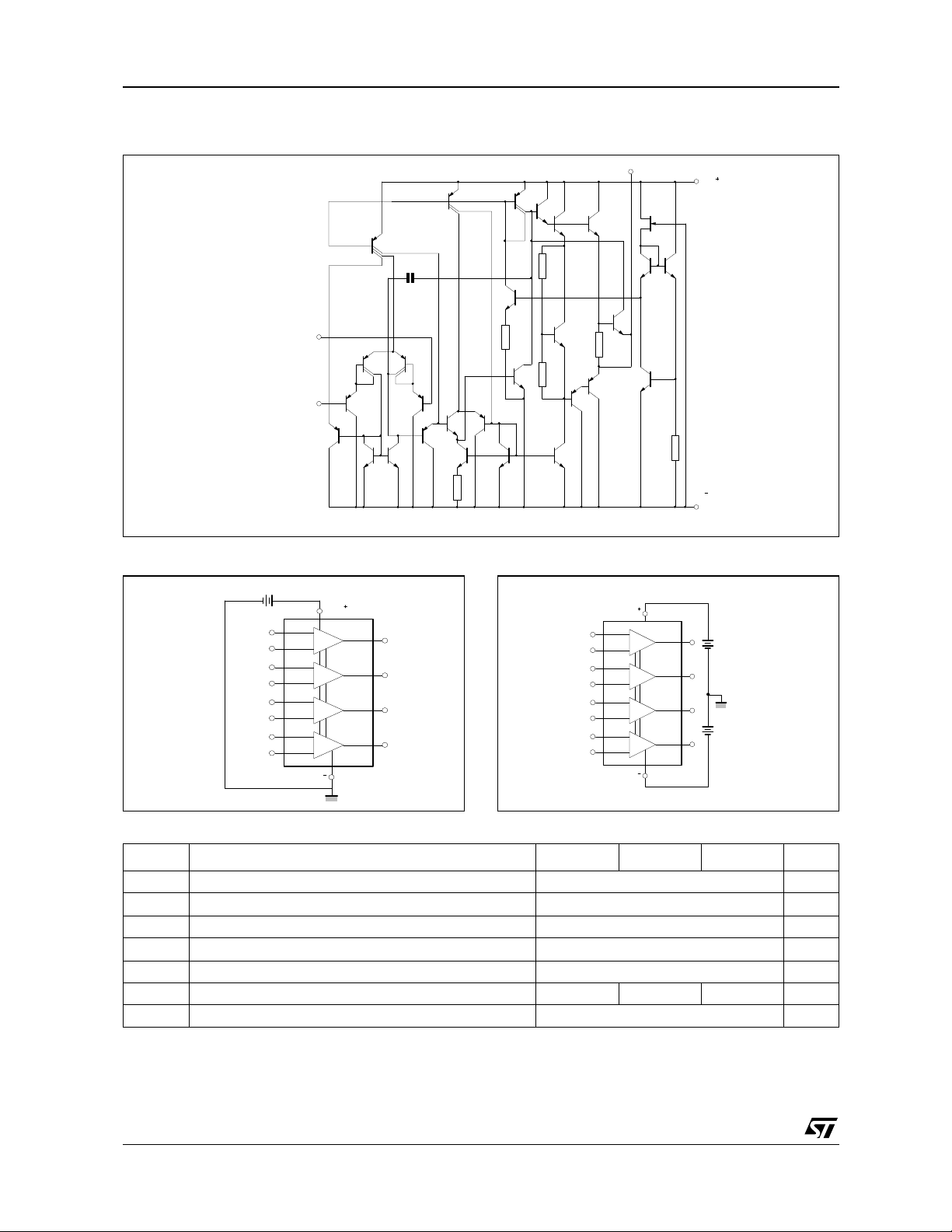
SCHEMATIC DIAGRAM (each amplifier)
Output
Q19
Q18
Q17
Q16
R4
Ω
31k
Q1
R6
Ω
0.7k
R2
37 k
Q9
Q7
Q8
Ω
Q10
Q13
Q11
Q12
Q15
R3
25
Ω
Non-inverting
input
Inverting
input
(1 stage)
Q23
Q22 Q24
Q21
Q2
Q3
Q20
C1
8pF
Q25
Q6
Q5
Q4
12k
Q14
R1
Ω
SCHEMATIC DIAGRAM DUAL SUPPLIES
Q27
Q28
Q30
8.2k
V
CC
Q29
R5
Ω
V
CC
(Ground)
ABSOLUTE MAXIMUM RATINGS
Symbol Parameter MC3503 MC3403 MC3303 Unit
V
P
T
T
1. For supply voltage less than ±15V, the absolute maximum input voltage is equal to the supply voltage.
2. Any of the amplifier outputs can be shorted to ground indefinitly; however more than one should not be simultaneously shorted as the maximum
2/10
Supply voltage ±18 or 36 V
CC
V
Input Voltage
i
V
Differential Input Voltage ±36 V
id
Output Short-circuit Duration
Power Dissipation 500 mW
tot
Operating Free-air Temperature Range -55 to +125 0 to +70 -40 to +105 °C
oper
Storage Temperature Range -65 to +150 °C
stg
junction will be exceeded.
1)
2)
±18 V
Infinite
MC3303 - MC3403 - MC3503
ELECTRICAL CHARACTERISTICS
V
= ±15V, T
CC
Symbol Parameter Min. Typ. Max. Unit
Input Offset Voltage (Rs ≤ 10kΩ)
V
io
Input Offset Current
I
io
Input Bias Current
I
ib
Large Signal Voltage Gain (Vo = ±10V, RL = 2k
A
vd
Supply Voltage Rejection Ratio (R
SVR
Supply Current, all Amp, no load
I
cc
Input Common Mode Voltage Range
V
icm
Common Mode Rejection Ratio (R
CMR
I
Output Short-circuit Current 10 30 45 mA
os
Output Voltage Swing
±V
opp
Slew Rate (V
SR
unity gain)
Rsie Time (Vo = ±20mV, RL = 2kΩ, CL = 100pF,T
t
r, tf
unity gain)
Overshoot (VI = ±20mV, RL = 2kΩ, CL = 100pF, T
K
OV
unity gain)
Z
Input Impedance 0.3 1
I
Z
Output Impedance 75
O
Power Bandwidth (RL = 2kΩ, CL = 100pF, AV = 1, T
B
om
V
O
Unity Gain Bandwidth V
B
25°C, unity gain)
= 25°C (unless otherwise specified)
amb
T
= 25°C
amb
T
≤ T
≤ T
amb
max
= 25°C
≤ T
≤ T
amb
max
= 25°C
≤ T
≤ T
amb
max
= 25°C
≤ T
≤ T
amb
max
≤ 10kΩ)
s
= 25°C
≤ T
≤ T
amb
max
= 25°C
≤ T
≤ T
amb
max
= 25°C
≤ T
≤ T
amb
max
≤ 10kΩ)
s
= 25°C
≤ T
≤ T
amb
max
= 25°C RL ≤ 10k
≤ T
≤ T
amb
max
= ±10V, RL = 2kΩ, CL = 100pF, T
I
T
T
T
T
T
T
T
T
T
T
T
T
T
T
min
amb
min
amb
min
amb
min
amb
min
amb
min
amb
min
T
T
amb
min
amb
min
= 2Vpp, THD ≤ 5%)
= 10mV, RL = 2kΩ, CL = 100pF, T
o
Ω)
MC3503
MC3503
R
≤ 2k
L
RL ≤ 10k
≤ 2k
R
L
= 25°C,
amb
amb
amb
Ω
Ω
Ω
Ω
= 25°C,
= 25°C,
= 25°C,
amb
amb
=
15
550
40 500
50
200 V/mV
25
77
90 dB
77
2.8 7
-15
-15
70
90 dB
70
12
10
13.5
13 V
12
10
0.35 0.5
0.18
10
9
1MHz
6
200
800
4
8
5
+13
+13
V/µs
ΜΩ
kHz
mV
nA
nA
mA
V
µs
%
Ω
3/10
 Loading...