

Low noise quad operational amplifier
Features
■ Low voltage noise: 4.5 nV/√Hz
■ High gain bandwidth product: 15 MHz
■ High slew rate: 7 V/µs
■ Low distortion: 0.002%
■ Large output voltage swing: +14.3 V/-14.6 V
■ Excellent frequency stability
■ ESD protection 2 kV
■ Macromodel included in this specification
Description
The MC33079 is a monolithic quad operational
amplifier particularly well suited for audio
applications.
It offers low voltage noise (4.5 nV/√Hz) and high
frequency performance (15 MHz gain bandwidth
product, 7 V/µs slew rate).
In addition the MC33079 has a v ery low distortion
(0.002%) and excellent phase/gain margins.
The output stage allows a large output voltage
swing and symmetrical source and sink currents.
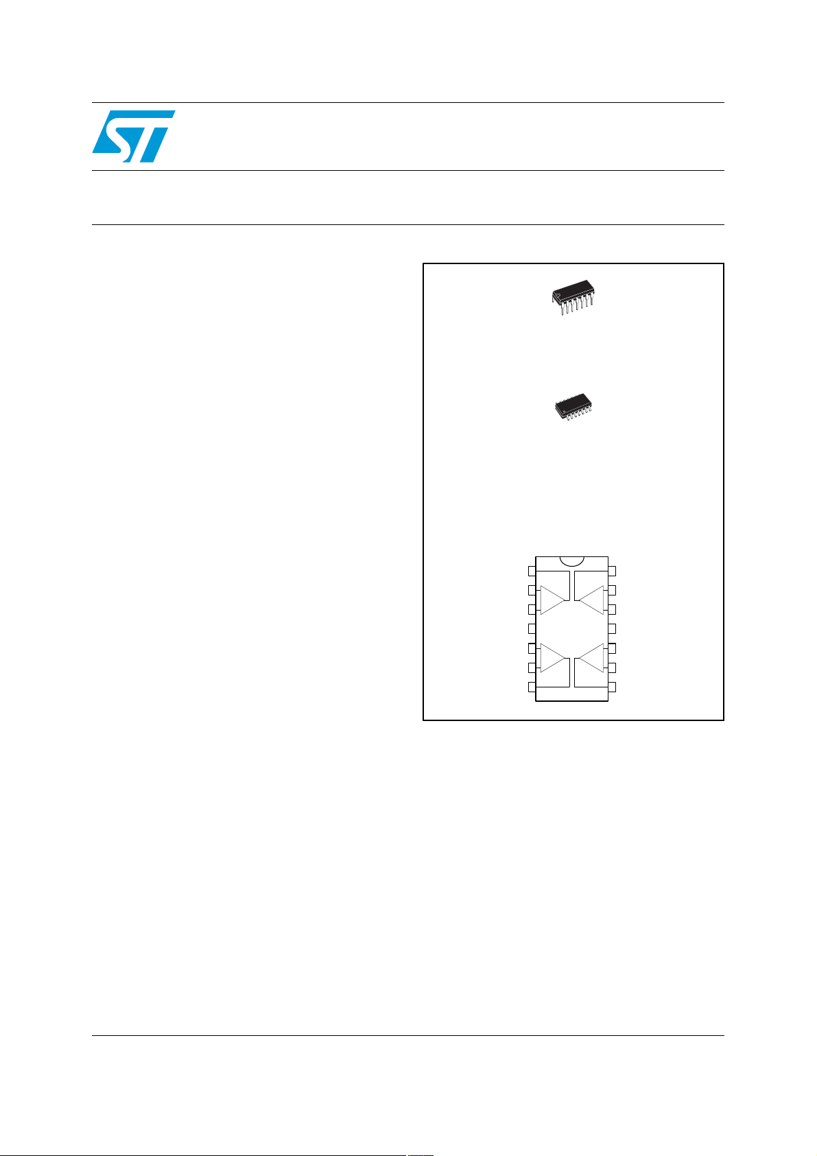
Output 1
Inverting Input 1
Non-inverting Input 1
V
CC
Non-inverting Input 2
Inverting Input 2
Output 2
MC33079
DIP14
(Plastic package)
SO-14
(Plastic micropackage)
Pin connections
(top view)
1
2
-
+
3
+
4
5
+
-
6
7
14
13
-
+
12
11
10
+
9
8
Output 4
Inverting Input 4
Non-inverting Input 4
-
V
CC
Non-inverting Input 3
Inverting Input 3
Output 3
March 2008 Rev 4 1/12
www.st.com
12

Schematic diagram (1/4 MC33079) MC33079
1 Schematic diagram (1/4 MC33079)
Figure 1. Schematic diagram (1/4 MC33079)
V
CC
Inverting
Input
Non-inverting
Input
V
CC
Output
2/12

MC33079 Absolute maximum ratings and operating conditions
2 Absolute maximum ratings and operating conditions
Table 1. Absolute maximum ratings (AMR)
Symbol Parameter Value Unit
V
V
Supply voltage ±18 or +36 V
CC
Differential input voltage
id
Input voltage
V
i
(1)
(1)
±30 V
±15 V
Output short-circuit duration Infinite s
T
Junction temperature +150 °C
j
T
R
R
ESD
1. Either or both input voltages must not exceed the magnitude of V
2. Short-circuits can cause excessive heating. Destructive dissipation can result from simultaneous shortcircuits on all amplifiers.
3. R
4. Human body model: 100pF discharged through a 1.5 kΩ resistor between two pins of the device, done for
all couples of pin combinations with other pins floating.
5. Machine model: a 200 pF cap is charged to the specified voltage, then discharged directly between two
pins of the device with no external series resistor (internal resistor < 5 Ω), done for all couples of pin
combinations with other pins floating.
6. Charged device model: all pins plus package are charged together to the specified voltage and then
discharged directly to the ground.
Table 2. Operating conditions
Storage temperature -65 to +150 °C
stg
(2) (3)
(2) (3)
CC
+
or V
CC
80
105
33
31
2kV
200 V
1.5 kV
-
.
Thermal resistance junction to ambient
thja
DIP14
SO-14
Thermal resistance junction to case
thjc
DIP14
SO-14
HBM: human body model
MM: machine model
(5)
CDM: charged device model
are typical values.
th
(4)
(6)
°C/W
°C/W
Symbol Parameter Value Unit
V
T
V
Supply voltage ±2.5 to ±15 V
CC
Operating free-air temperature range -40 to 105 °C
oper
Input common mode voltage range (ΔVio= 5mV, Vo= 0V) ±13 to ±14 V
icm
3/12
Electrical characteristics MC33079
3 Electrical characteristics
Table 3. V
+
= +15V, V
CC
Symbol Parameter Min. Typ. Max. Unit
-
= -15V, T
CC
= 25°C (unless otherwise specified)
amb
V
DV
A
Input offset voltage (Vo = 0V, Vic = 0V)
io
≤ T
T
min
amb
≤ T
max
Input offset voltage drift
io
I
io
I
ib
= 0V, Vic = 0V, T
V
o
min
≤ T
amb
≤ T
Input offset current (Vo = 0V, Vic = 0V)
≤ T
T
min
amb
≤ T
max
Input bias current (Vo = 0V, Vic = 0V)
≤ T
T
min
amb
≤ T
max
Large signal voltage gain (RL = 2kΩ, Vo = ±10V)
vd
≤ T
T
min
amb
≤ T
max
max
2µV/°C
10 150
250 750
9085100
2.5
3.5
175
800
Output voltage swing (Vid = ±1V)
RL = 600Ω
= 600Ω
R
±V
opp
L
RL = 2.0kΩ
RL = 2.0kΩ
= 10kΩ
R
L
RL = 10kΩ
CMR Common-mode rejection ratio (V
SVR Supply voltage rejection ratio (V
13.2
13.5
= ±13V) 80 100 dB
ic
+
-
/ V
CC
= +15V / -15V to +5V / -5V) 80 105 dB
CC
12.2
-12.7
14
-14.2
14.3
-14.6
-13.2
-14
Output short-circuit current (Vid = ±1V, output to ground)
I
o
I
CC
SR Slew rate (V
GBP Gain bandwidth product (R
Source
Sink
Supply current (Vo = 0V, all amplifiers)
≤ T
T
min
≤ T
amb
max
= -10V to +10V, RL = 2kΩ, CL = 100pF, AV = +1) 5 7 V/µs
i
= 2kΩ, CL = 100pF, f = 100kHz) 10 15 MHz
L
15
20
29
37
810
12
B Unity gain bandwidth (open loop) 9 MHz
Gain margin (RL = 2kΩ)
A
m
= 0pF
C
L
CL = 100pF
-11
-6
mV
nA
nA
dB
V
mA
mA
dB
Phase margin (R
φm
e
i
n
n
CL = 0pF
= 100pF
C
L
Equivalent input noise voltage (RS = 100Ω, f = 1kHz) 4.5
Equivalent input noise current (f = 1kHz) 0.5
= 2kΩ)
L
4/12
55
30
Degrees
nV
----------- Hz
pA
----------- Hz
 Loading...