

Features
1
2
3
45
6
7
8
-
+
-
+
Output 1
Inverting input 1
Non-inverting input 1
V
CC
V
CC
Output 2
Inverting input 2
Non-inverting input 2
-
+
■ Low voltage noise: 4.5 nV/√Hz
■ High gain bandwidth product: 15 MHz
■ High slew rate: 7V/µs
■ Low distortion: 0.002%
■ Large output voltage swing: +14.3 V / -14.6 V
■ Low input offset voltage
■ Excellent frequency stability
■ ESD protection 2 kV
■ Macromodel included in this specification
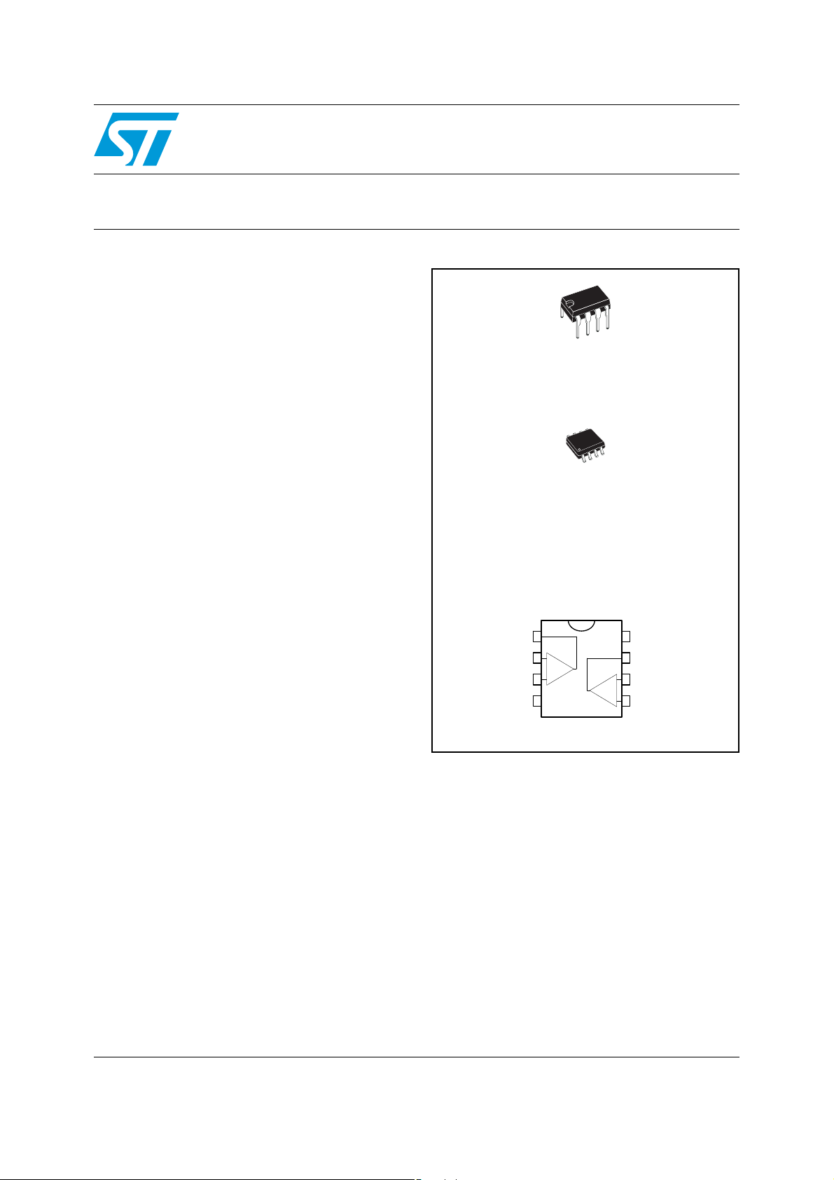
Description
MC33078
Low noise dual operational amplifier
N
DIP8
(Plastic package)
D
SO-8
(Plastic micropackage)
The MC33078 is a monolithic dual operational
amplifier particularly well suited for audio
applications.
It offers low voltage noise (4.5 nV/√Hz) and high
frequency performance (15 MHz gain bandwidth
product, 7 V/µs slew rate).
In addition, the MC33078 has a very low
distortion (0.0 02%) an d excellent phase/ga in
margins.
The output stage allows a large output voltage
swing and symmetrical source and sink currents.
Pin connections (top view)
March 2008 Rev 5 1/15
www.st.com
15
Absolute maximum ratings and operating conditions MC33078
1 Absolute maximum ratings and operating conditions
Table 1. Absolute maximum ratings (AMR)
Symbol Parameter Value Unit
V
V
Supply voltage ±18 or +36 V
CC
Differential input voltage - note
id
Input voltage - see note 1 ±15 V
V
i
(1)
±30 V
Output short circuit duration Infinite s
T
Junction temperature +150 °C
j
T
R
R
ESD
1. Either or both input voltages must not exceed the magnitude of V
2. Short-circuits can cause excessive heating and destructive dissipation.
3. R
4. Human body model: A 100 pF capacitor is charged to the specified voltage, then discharged through a
1.5 kΩ resistor between two pins of the device. This is done for all couples of connected pin combinations
while the other pins are floating.
5. Machine model: A 200pF capacitor is charged to the specified voltage, then discharged directly between
two pins of the device with no external series resistor (internal resistor < 5 Ω). This is done for all couples of
connected pin combinations while the other pins are floating.
6. Charged device model: all pins and the package are charged together to the specified voltage and then
discharged directly to the ground through only one pin. This is done for all pins.
Table 2. Operating conditions
Storage temperature -65 to +150 °C
stg
(2) (3)
(2) (3)
CC
+
or V
125
85
40
41
2kV
200 V
1.5 kV
-
.
CC
Thermal resistance junction to ambient
thja
SO-8
DIP8
Thermal resistance junction to case
thjc
SO-8
DIP8
HBM: human body model
MM: machine model
(5)
CDM: charged device model
are typical values.
th
(4)
(6)
°C/W
°C/W
Symbol Parameter Value Unit
V
T
Supply voltage ±2.5 to ±15 V
CC
Operating free-air temperature range -40 to 105 °C
oper
2/15
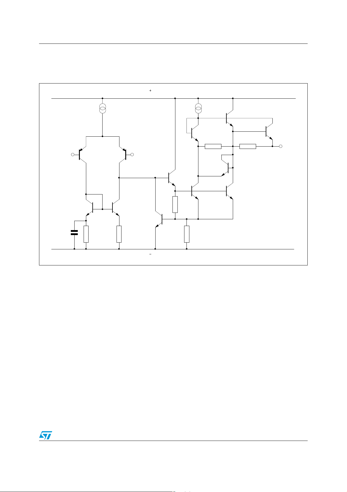
MC33078 Schematic diagram
2 Schematic diagram
Figure 1. Schematic diagram (1/2 MC33078)
V
CC
Inverting
Input
Non-inverting
Input
V
CC
Output
3/15
Electrical characteristics MC33078
3 Electrical characteristics
Table 3. V
+
= +15V, V
CC
Symbol Parameter Min. Typ. Max. Unit
-
= -15V, T
CC
= 25°C (unless otherwise specified)
amb
V
DV
V
A
Input offset voltage (Vo = 0V, Vic = 0V)
io
≤ T
T
min
amb
≤ T
max
Input offset voltage drift
I
I
icm
io
io
ib
= 0V, Vic = 0V, T
V
o
min
≤ T
amb
≤ T
max
Input offset current (Vo = 0V, Vic = 0V)
≤ T
T
min
amb
≤T
max
Input bias current (Vo = 0V, Vic = 0V)
≤ T
T
min
amb
≤ T
max
Input common mode voltage range (ΔVio = 5mV, Vo = 0V) ±13 ±14 V
Large signal voltage gain (RL = 2kΩ, Vo = ±10V)
vd
≤ T
T
min
amb
≤ T
max
0.15 2
3
2µV/°C
10 150
175
250 750
800
9085100
Output voltage swing (Vid = ±1V)
= 600Ω
R
L
RL = 600Ω
±V
opp
RL = 2.0kΩ
= 2.0kΩ
R
L
RL = 10kΩ
RL = 10kΩ
CMR Common-mode rejection ratio (V
SVR
Supply voltage rejection ratio
+
-
/ V
V
CC
= +15V / -15V to +5V / -5V
CC
13.2
13.5
= ±13V) 80 100 dB
ic
12.2
-12.7
14
-14.2
-13.2
14.3
-14.6
-14
80 105 dB
Output short-circuit current (Vid = ±1V, output to ground)
I
o
I
CC
SR
GBP
Source
Sink
Supply current (Vo = 0V, all amplifiers)
≤ T
T
min
amb
≤ T
max
Slew rate
= -10V to +10V, RL = 2kΩ, CL = 100pF, AV = +1
V
i
Gain bandwidth product
R
= 2kΩ, CL = 100pF, f = 100kHz
L
15
20
29
37
45
5.5
57 V/µs
10 15 MHz
B Unity gain bandwidth (Open loop) 9 MHz
mV
nA
nA
dB
V
mA
mA
A
φm
Gain margin (RL = 2kΩ), CL = 0pF
m
CL = 100pF
Phase margin (R
= 100pF
C
L
Equivalent input noise voltage
e
n
RS = 100Ω, f = 1kHz
i
Equivalent input noise current (f = 1kHz) 0.5 pA/√Hz
n
= 2kΩ), CL = 0pF
L
4/15
-11
-6
55
30
Degrees
4.5 nV/
dB
√Hz
MC33078 Electrical characteristics
Table 3. V
+
= +15V, V
CC
-
= -15V, T
CC
= 25°C (unless otherwise specified) (continued)
amb
Symbol Parameter Min. Typ. Max. Unit
THD
VO1/V
FPB
Total harmonic distortion
= 2kΩ, f = 20Hz to 20kHz, Vo = 3V
R
L
Channel separation
O2
f = 20Hz to 20kHz
Full power bandwidth
V
= 27Vpp, RL = 2kΩ, THD ≤ 1%
o
Output impedance
Z
o
R
i
C
i
= 0V, f = 9MHz
V
o
Input resistance
Vic = 0V
Input capacitance
Vic = 0V
, AV = +1
rms
0.002 %
120 dB
120 kHz
37 Ω
175 kΩ
12 pF
5/15

Electrical characteristics MC33078
Figure 2. Total supply current vs. supply
voltage
5
4.5
4
3.5
3
2.5
2
1.5
Total Supply Current (mA)
1
0.5
0
0 5 10 15 20 25 30
Supply Voltage (V)
Figure 4. Equivalent input noise v oltage vs.
frequency
VCC = ±15V, G = 100
= 100, T
R
s
amb
= 25°C
Figure 3. Output voltage vs. supply voltage
15
10
5
0
-5
Output Voltage (V)
-10
-15
0 5 10 15
Supply Voltage (V)
Figure 5. Output short circuit current vs.
output voltage
50
40
30
20
10
0
-10
-20
Output Short Circuit Current (mA)
-30
-40
0102030
VCC = 0/30V
= 25°C
T
amb
Output Voltage ( V)
Figure 6. Output voltage vs. supply voltage Figure 7. THD + noise vs. frequency
15
10
5
0
-5
Output Voltage (V)
-10
-15
0 5 10 15
Supply Voltage (V)
Vid = ±1V
= 2kΩ
R
L
6/15
1
0.1
0.01
THD+Noise (%)
0.001
0.01 0.1 1 10 100
RL = 2kΩ, Vo = 3V
VCC = ±15V, Av = 1
Frequency ( k Hz)
rms

MC33078 Electrical characteristics
Figure 8. Voltage gain and phase vs.
frequency
50
40
30
20
10
Gain (dB)
0
-10
-20
-30
10 100 1000 10000 100000
RL = 2kΩ, CL = 100pF
V
= ±15V, G = -100
CC
Frequency (kHz)
Figure 9. THD noise vs. V
180
120
60
0
-60
-120
1.000
0.100
Phase (Deg)
0.010
THD+Noise (%)
0.001
V
12345678910
out
RL = 2kΩ, f = 1kHz
= ±15V, Av = 10
CC
Vout (Vrms)
7/15

Macromodel MC33078
4 Macromodel
4.1 Important note concerning this macromodel
Please consider the following remarks before using this macromodel.
● All models are a trade-off between accuracy and complexity (i.e. simulation time).
● Macromodels are not a substitute to breadboarding; rather, they confirm the validity of
a design approach and help to select surrounding component values.
● A macromodel emulates the nominal p erf ormance of a typical de vice within specified
operating conditions (temperature, supply voltage, for e xample). Thus the
macromodel is often not as exhaustive as the datasheet, its purpose is to illustrate the
main parameters of the product.
Data derived from macromodels used outside of the specified conditions (V
for example) or even worse, outside of the device operating conditions (V
CC
example), is not reliable in any way.
Section 4.2 provides the electrical characteristics resulting f r om the u se of t his macro mod el.
4.2 Electrical characteristics from macromodelization
Table 4. Electrical characterist ics resulting from macromodel simulation at
Symbol Conditions Value Unit
V
io
A
VD
I
CC
V
icm
V
opp
I
sink
I
source
GBP R
SR R
φmR
+
V
= +15V, VCC- = -15V, T
CC
= 25°C (unless otherwise specified)
amb
0mV
RL = 2kΩ, VO = ±10V 100 dB
No load, per operator 2 mA
ΔV
= 5mV, VO = 0V 28 V
io
RL = 2kΩ 28.2 V
VO = 0V 37 mA
VO = 0V 29 mA
= 2kΩ, CL = 100pF 15 MHz
L
= 10kΩ, CL = 100pF, AV = +1 7 V/µs
L
= 2kΩ, CL = 0pF 55 Degrees
L
, temperature,
CC
, V
, for
icm
8/15

MC33078 Macromodel
4.3 Macromodel code
** Standard Linear Ics Macromodels, 1993.
** CONNECTIONS :
* 1 INVERTING INPUT
* 2 NON-INVERTING INPUT
* 3 OUTPUT
* 4 POSITIVE POWER SUPPLY
* 5 NEGATIVE POWER SUPPLY
.SUBCKT MC33078 1 3 2 4 5
********************************************************
.MODEL MDTH D IS=1E-8 KF=2.286238E-16 CJO=10F
* INPUT STAGE
CIP 2 5 1.200000E-11
CIN 1 5 1.200000E-11
EIP 10 5 2 5 1
EIN 16 5 1 5 1
RIP 10 11 2.363636E+00
RIN 15 16 2.363636E+00
RIS 11 15 1.224040E+01
DIP 11 12 MDTH 400E-12
DIN 15 14 MDTH 400E-12
VOFP 12 13 DC 0
VOFN 13 14 DC 0
IPOL 13 5 1.100000E-04
CPS 11 15 2.35E-09
DINN 17 13 MDTH 400E-12
VIN 17 5 1.000000e+00
DINR 15 18 MDTH 400E-12
VIP 4 18 1.000000E+00
FCP 4 5 VOFP 1.718182E+01
FCN 5 4 VOFN 1.718182E+01
FIBP 2 5 VOFN 4.545455E-03
FIBN 5 1 VOFP 4.545455E-03
* AMPLIFYING STAGE
FIP 5 19 VOFP 9.545455E+02
FIN 5 19 VOFN 9.545455E+02
CC 19 29 1.500000E-08
HZTP 30 29 VOFP 1.523529E+02
HZTN 5 30 VOFN 1.523529E+02
DOPM 51 22 MDTH 400E-12
DONM 21 52 MDTH 400E-12
HOPM 22 28 VOUT 5.172414E+03
VIPM 28 4 1.500000E+02
HONM 21 27 VOUT 4.054054E+03
VINM 5 27 1.500000E+02
DBIDON1 19 53 MDTH 400E-12
V1 51 53 0.68
DBIDON2 54 19 MDTH 400E-12
V2 54 52 0.68
RG11 51 5 3.04E+05
RG12 51 4 3.04E+05
9/15

Macromodel MC33078
RG21 52 5 0.6072E+05
RG22 52 4 0.6072E+05
E1 50 40 51 0 1 E2 40 39 52 0 1
EDEC1 38 39 4 0 0.5
EDEC2 0 38 5 0 0.5
DOP 51 25 MDTH 400E-12
VOP 4 25 1.474575E+00
DON 24 52 MDTH 400E-12
VON 24 5 1.474575E+00
RAJUS 50 5 1E12
GCOMP 5 4 4 5 8.1566068E-04
RPM1 5 80 1E+06
RPM2 4 80 1E+06
GAVPH 5 82 50 80 3.26E-03
RAVPHGH 82 4 613
RAVPHGB 82 5 613
RAVPHDH 82 83 1000
RAVPHDB 82 84 1000
CAVPHH 4 83 0.159E-09
CAVPHB 5 84 0.159E-09
EOUT 26 23 82 5 1
VOUT 23 5 0
ROUT 26 3 4.780354E+01
COUT 3 5 1.000000E-12
.ENDS
10/15

MC33078 Package information
5 Package information
In order to meet environmental requ irements, ST offers these devices in ECOPACK®
packages. These packages have a lead-free second level interconnect. The category of
second level interconnect is marked on the package and on the inner box label, in
compliance with JEDEC Standard JESD97. The maximum ratings related t o soldering
conditions are also marked on the inner box label. ECOPACK is an ST trademark.
ECOPACK specifications are available at: www.st.com
.
11/15

Package information MC33078
5.1 DIP8 package information
Figure 10. DIP8 package mechanical drawing
Table 5. DIP8 package mechanical data
Dimensions
Ref.
Min. Typ. Max. Min. Typ. Max.
A5.330.210
A1 0.38 0.015
A2 2.92 3.30 4.95 0.115 0.130 0.195
b 0.36 0.46 0.56 0.014 0.018 0.022
b2 1.14 1.52 1.78 0.045 0.060 0.070
c 0.20 0.25 0.36 0.008 0.010 0.014
D 9.02 9.27 10.16 0.355 0.365 0.400
E 7.62 7.87 8.26 0.300 0.310 0.325
E1 6.10 6.35 7.11 0.240 0.250 0.280
e 2.54 0.100
eA 7.62 0.300
eB 10.92 0.430
L 2.92 3.30 3.81 0.115 0.130 0.150
Millimeters Inches
12/15

MC33078 Package information
5.2 SO-8 package information
Figure 11. SO-8 package mechanical drawing
Table 6. SO-8 package mechanical data
Dimensions
Ref.
Min. Typ. Max. Min. Typ. Max.
A1.750.069
A1 0.10 0.25 0.004 0.010
A2 1.25 0.049
b 0.28 0.48 0.011 0.019
c 0.17 0.23 0.007 0.010
D 4.80 4.90 5.00 0.189 0.193 0.197
E 5.80 6.00 6.20 0.228 0.236 0.244
E1 3.80 3.90 4.00 0.150 0.154 0.157
e 1.27 0.050
h 0.25 0.50 0.010 0.020
L 0.40 1.27 0.016 0.050
k1°8°1°8°
ccc 0.10 0.004
Millimeters Inches
13/15

Ordering information MC33078
6 Ordering information
Table 7. Order codes
Order code
Temperature
MC33078N
MC33078D
MC33078DT
MC33078YD
MC33078YDT
1. Qualification and characterization according to AEC Q100 and Q003 or equivalent, advanced screening
according to AEC Q001 & Q 002 or equivalent are on-going.
(1)
(1)
-40, +105°C
7 Revision history
Table 8. Document revision history
Date Revision Changes
10-Nov-2001 1 Initial release.
10-Jun-2005 2 PPAP references inserted in the datasheet, see order codes table.
30-Sep- 2005 3
16-Feb-2006 4 Corrected error in the first page title.
range
Package Packing Marking
DIP8 Tube MC33078N
SO-8
SO-8
(Automotive grade)
Tube or
Tape & reel
Tube or
Tape & reel
The following changes were made in this revision:
– Order codes table updated with complete list of mar k ings and
packages.
– Reorgani zation of Chapter 4.3: Macromodel code on page 9.
33078
33078Y
and ESD values in absolute maximum ratings table.
th
3-Mar-2008 5
Added R
Added footnote for automotive grade order codes in order codes
table.
Re-formatted document.
14/15

MC33078
Please Read Carefully:
Information in this document is provided solely in connection with ST products. STMicroelectronics NV and its subsidiaries (“ST”) reserve the
right to make changes, corrections, modifications or improvements, to this document, and the products and services described herein at any
time, without notice.
All ST products are sold pursuant to ST’s terms and conditions of sale.
Purchasers are solely res ponsibl e fo r the c hoic e, se lecti on an d use o f the S T prod ucts and s ervi ces d escr ibed he rein , and ST as sumes no
liability whatsoever relati ng to the choice, selection or use of the ST products and services described herein.
No license, express or implied, by estoppel or otherwise, to any intellectual property rights is granted under this document. If any part of this
document refers to any third pa rty p ro duc ts or se rv ices it sh all n ot be deem ed a lice ns e gr ant by ST fo r t he use of su ch thi r d party products
or services, or any intellectua l property c ontained the rein or consi dered as a warr anty coverin g the use in any manner whats oever of suc h
third party products or servi ces or any intellectual property contained therein.
UNLESS OTHERWISE SET FORTH IN ST’S TERMS AND CONDITIONS OF SALE ST DISCLAIMS ANY EXPRESS OR IMPLIED
WARRANTY WITH RESPECT TO THE USE AND/OR SALE OF ST PRODUCTS INCLUDING WITHOUT LIMITATION IMPLIED
WARRANTIES OF MERCHANTABILITY, FITNESS FOR A PARTICUL AR PURPOS E (AND THEIR EQUIVALE NTS UNDER THE LAWS
OF ANY JURISDICTION), OR INFRINGEMENT OF ANY PATENT, COPYRIGHT OR OTHER INTELLECTUAL PROPERTY RIGHT.
UNLESS EXPRESSLY APPROVED IN WRITING BY AN AUTHORIZED ST REPRESENTATIVE, ST PRODUCTS ARE NOT
RECOMMENDED, AUTHORIZED OR WARRANTED FOR USE IN MILITARY, AIR CRAFT, SPACE, LIFE SAVING, OR LIFE SUSTAINING
APPLICATIONS, NOR IN PRODUCTS OR SYSTEMS WHERE FAILURE OR MALFUNCTION MAY RESULT IN PERSONAL INJ URY,
DEATH, OR SEVERE PROPERTY OR ENVIRONMENTAL DAMAGE. ST PRODUCTS WHICH ARE NOT SPECIFIED AS "AUTOMOTIVE
GRADE" MAY ONLY BE USED IN AUTOMOTIVE APPLICATIONS AT USER’S OWN RISK.
Resale of ST products with provisions different from the statements and/or technical features set forth in this document shall immediately void
any warranty granted by ST fo r the ST pro duct or serv ice describe d herein and shall not cr eate or exten d in any manne r whatsoever , any
liability of ST.
ST and the ST logo are trademarks or registered trademarks of ST in various countries.
Information in this document su persedes and replaces all information previously supplied.
The ST logo is a registered trademark of STMicroelectronics. All other names are the property of their respective owners.
© 2008 STMicroelectronics - All rights reserved
STMicroelectronics group of compan ie s
Australia - Belgium - Brazil - Canada - China - Czech Republic - Finland - France - Germany - Hong Kong - India - Israel - Italy - Japan -
Malaysia - Malta - Morocco - Singapore - Spain - Sweden - Switzerland - United Kingdom - United States of America
www.st.com
15/15
 Loading...