


Inverting Input 2
Non-inverting Input 2
Non-inverting Input 1
CC
V
-
CC
V
1
2
3
4
8
5
6
7
9
10
11
12
13
14
+
Output 3
Output 4
Non-inverting Input 4
Inverting Input 4
Non-inverting Input 3
Inverting Input 3
-
+
+
-
+
-
+
Output 1
Inverting Input 1
Output 2
MC3303
MC3403 - MC3503
LOW POWER
QUAD BIPOLAR OPERATIONAL AMPLIFIERS
■ SHORT-CIRCUIT PROTECTED OUTPUTS
■ CLASS AB OUTPUT STAGE FOR MINIMAL
CROSSOVER DISTORTION
■ SINGLE SUPPLY OPER ATION: +3V TO +36V
■ DUAL SUPPLIES: ±15V TO ±18V
■ LOW INPUT BIAS CURRENT: 500nA MAX
■ INTERNALLY COMPENSATED
■ SIMILAR PERFORMANCE TO POPULAR
UA741
DESCRIPTION
The MC3403 is a low-cos t, quad operational amplifier with true differential i nputs. The devic e has
electrical characteristics similar to the popular
UA741. However the MC3403, has several distinct advantages over standa rd operat iona l am plifiers types in single supply applications. The quad
amplifier can operate at supply voltage as low as 3
Volts or as high as 36 volts with quiescent currents
about one third of those associated with the
UA741 (on a per amplifier basis). The common-mode input range includes the negat ive sup ply, thereby eliminating the neces sity for external
biasing components in many applications.
N
DIP14
(Plastic Package)
(Plastic Micropackage)
P
TSSOP14
(Thin Shrink Small Outline Package)
PIN CONNECTIONS (top view)
D
SO14
ORDER CODE
Part
Number
Temperature
Range
MC3303 -40°C, +105°C
MC3403 0°C, +70°C
MC3503 -55°C, +125°C
Example : MC3403N
N = Dual in Line Package (DIP)
D = Small Outline Package (SO) - also available in Tape & Reel (DT)
P = Thin Shrink Small Outline Package (TSSOP) - only available
in Tape & Reel (PT)
November 2001
Package
NDP
•••
•••
•••
1/10
MC3303 - MC3403 - MC3503
V
CC
V
CC
+3V to +30V
1.5V to 18V
1.5V to 18V
V
CC
V
CC
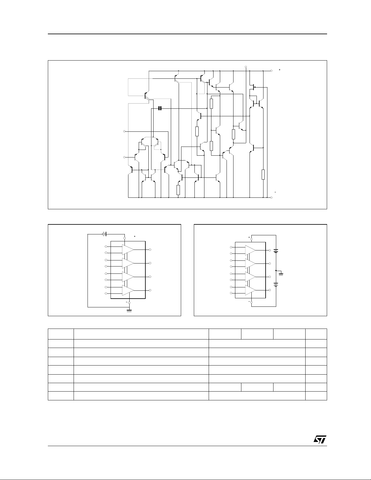
SCHEMATIC DIAGRAM (each amplifier)
Output
Q19
Q18
Q17
Q16
R4
Ω
31k
Q1
R6
Ω
0.7k
R2
37 k
Q9
Q7
Q8
Ω
Q10
Q13
Q11
Q12
Q15
R3
25
Ω
Non-inverting
input
Inverting
input
(1 stage)
Q23
Q22 Q24
Q21
Q2
Q3
Q20
C1
8pF
Q25
Q6
Q5
Q4
12k
Q14
R1
Ω
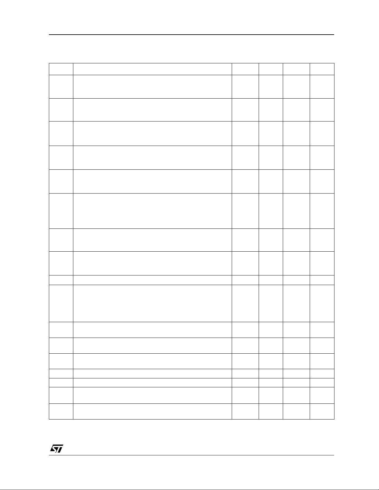
SCHEMATIC DIAGRAM DUAL SUPPLIES
Q27
Q28
Q30
8.2k
V
CC
Q29
R5
Ω
V
CC
(Ground)
ABSOLUTE MAXIMUM RATINGS
Symbol Parameter MC3503 MC3403 MC3303 Unit
V
P
T
T
1. For supply voltage less than ±15V, the absolute maximum input voltage is equal to the supply voltage.
2. Any of the amplifier outputs can be shorted to ground indefinitly; however more than one should not be simultaneously shorted as the maximum
2/10
Supply voltage ±18 or 36 V
CC
V
Input Voltage
i
V
Differential Input Voltage ±36 V
id
Output Short-circuit Duration
Power Dissipation 500 mW
tot
Operating Free-air Temperature Range -55 to +125 0 to +70 -40 to +105 °C
oper
Storage Temperature Range -65 to +150 °C
stg
junction will be exceeded.
1)
2)
±18 V
Infinite
MC3303 - MC3403 - MC3503
ELECTRICAL CHARACTERISTICS
V
= ±15V, T
CC
Symbol Parameter Min. Typ. Max. Unit
Input Offset Voltage (Rs ≤ 10kΩ)
V
io
Input Offset Current
I
io
Input Bias Current
I
ib
Large Signal Voltage Gain (Vo = ±10V, RL = 2k
A
vd
Supply Voltage Rejection Ratio (R
SVR
Supply Current, all Amp, no load
I
cc
Input Common Mode Voltage Range
V
icm
Common Mode Rejection Ratio (R
CMR
I
Output Short-circuit Current 10 30 45 mA
os
Output Voltage Swing
±V
opp
Slew Rate (V
SR
unity gain)
Rsie Time (Vo = ±20mV, RL = 2kΩ, CL = 100pF,T
t
r, tf
unity gain)
Overshoot (VI = ±20mV, RL = 2kΩ, CL = 100pF, T
K
OV
unity gain)
Z
Input Impedance 0.3 1
I
Z
Output Impedance 75
O
Power Bandwidth (RL = 2kΩ, CL = 100pF, AV = 1, T
B
om
V
O
Unity Gain Bandwidth V
B
25°C, unity gain)
= 25°C (unless otherwise specified)
amb
T
= 25°C
amb
T
≤ T
≤ T
amb
max
= 25°C
≤ T
≤ T
amb
max
= 25°C
≤ T
≤ T
amb
max
= 25°C
≤ T
≤ T
amb
max
≤ 10kΩ)
s
= 25°C
≤ T
≤ T
amb
max
= 25°C
≤ T
≤ T
amb
max
= 25°C
≤ T
≤ T
amb
max
≤ 10kΩ)
s
= 25°C
≤ T
≤ T
amb
max
= 25°C RL ≤ 10k
≤ T
≤ T
amb
max
= ±10V, RL = 2kΩ, CL = 100pF, T
I
T
T
T
T
T
T
T
T
T
T
T
T
T
T
min
amb
min
amb
min
amb
min
amb
min
amb
min
amb
min
T
T
amb
min
amb
min
= 2Vpp, THD ≤ 5%)
= 10mV, RL = 2kΩ, CL = 100pF, T
o
Ω)
MC3503
MC3503
R
≤ 2k
L
RL ≤ 10k
≤ 2k
R
L
= 25°C,
amb
amb
amb
Ω
Ω
Ω
Ω
= 25°C,
= 25°C,
= 25°C,
amb
amb
=
15
550
40 500
50
200 V/mV
25
77
90 dB
77
2.8 7
-15
-15
70
90 dB
70
12
10
13.5
13 V
12
10
0.35 0.5
0.18
10
9
1MHz
6
200
800
4
8
5
+13
+13
V/µs
ΜΩ
kHz
mV
nA
nA
mA
V
µs
%
Ω
3/10
MC3303 - MC3403 - MC3503
Symbol Parameter Min. Typ. Max. Unit
GBP
THD
DV
V
o1/Vo2
Gain Bandwith Product (V
f =100kHz, T
= 25°C)
amb
Total Harmonic Distortion (f = 1kHz, A
= 100pF, Vo = 2Vpp, T
C
L
Equivalent Input Noise Voltage (f = 1kHz, Rs = 100
e
n
m Phase Margin 60 Degrees
φ
Input Offset Voltage Drift
DI
io
io
T
≤ T
amb
≤ T
min
Input Offset Current Drift
≤ T
T
min
amb
≤ T
Channel Separation 120 dB
= 10 mV, RL = 2kΩ, CL = 100pF
O
0.7 1
= 20dB, RL = 2k
= 25°C) 0.02
amb
v
Ω
Ω
max
max
43
10
50
MHz
----------- -
µV/°C
pA/°C
%
nV
Hz
ELECTRICAL CHARACTERISTICS
+
V
= 5V, V
CC
Symbol Parameter Min. Typ. Max. Unit
V
io
I
io
I
ib
A
vd
SVR
I
cc
V
opp
-
= Ground, T
CC
= 25°C (unless otherwise specified)
amb
Input Offset Voltage (Rs ≤ 10kΩ)
T
= 25°C
amb
T
≤ T
amb
≤ T
max
min
Input Offset Current
= 25°C
T
amb
T
≤ T
amb
= 25°C
≤ T
amb
≤ T
≤ T
max
max
min
Input Bias Current
T
amb
T
min
Large Signal Voltage Gain (Vo = 1.4Vto 2.4V, RL = 2k
T
= 25°C
amb
T
≤ T
amb
= 25°C
≤ T
amb
≤ T
≤ T
max
max
≤ 10kΩ)
s
min
Supply Voltage Rejection Ratio (R
T
amb
T
min
Supply Current, all Amp, no load
MC3503 2.8
Output Voltage Range (RL = 10k
V
= +5V
CC
+5 < V
≤ +30V
CC
Ω)
Ω)
15
6
550
200
40 500
800
10
200 V/mV
5
77
90 dB
77
7
4
3.3
+
V
-2V
CC
3.5
+
V
-1.7V
CC
mV
nA
nA
mA
V
4/10
CIRCUIT DESCRIPTION
1/4
MC3403
V
O
V
CC
V
CC
R1
10kΩ
V
O
=
V
CC
1
2
V
O
R1
R1 + R2
V
CC
=
R2
10kΩ
50kΩ
5kΩ
10kΩ
1/4
MC3403
V
O
V
CC
V
(ref)
R
C
C
R
V
(ref)
=
1
2
V
CC
f
O
=
1
2 π RC
For
f
O
= 1kHz
R = 16kΩ
C = 0.01µF
The MC3403 i s made usin g four internally compensated, two-stage operational amplifiers. The
first stage of each consists of differential input devices Q24 and Q22 with input buffer transistors
Q25 and Q21 and the differential to single ended
converter Q3 and Q4. The first stage performs not
only the first stage gain function but also performs
the level shifting and transonductance reduction
functions. By reducing the transconductance a
smaller compensation capacitor (only 8pF) can be
employed, thus saving chip area.
The transconductance reduc tion is accomplished
by splitting the collectors of Q24 and Q22. Another
feature of this input stage is that the input common-mode range can include the negative supply
fo ground, in single supply ope ration, without saturation either the inpu t devices or the differential
to single-ended converter.
The second st age consists of a standard c urrent
source load amplifier stage. The output stage is
unique because it allows the output to swing to
ground in single supply operation and yet does not
exhibit any crossover disto rtion in split supply operations. This is possible because class AB operation is utilized.
Each amplifier is biased from an internal voltage
regulator which has a low temperature coef ficient
thus giving each amplifier good temperature characteristics as we ll as excellent power suppl y rejection.
MC3303 - MC3403 - MC3503
AV = 100
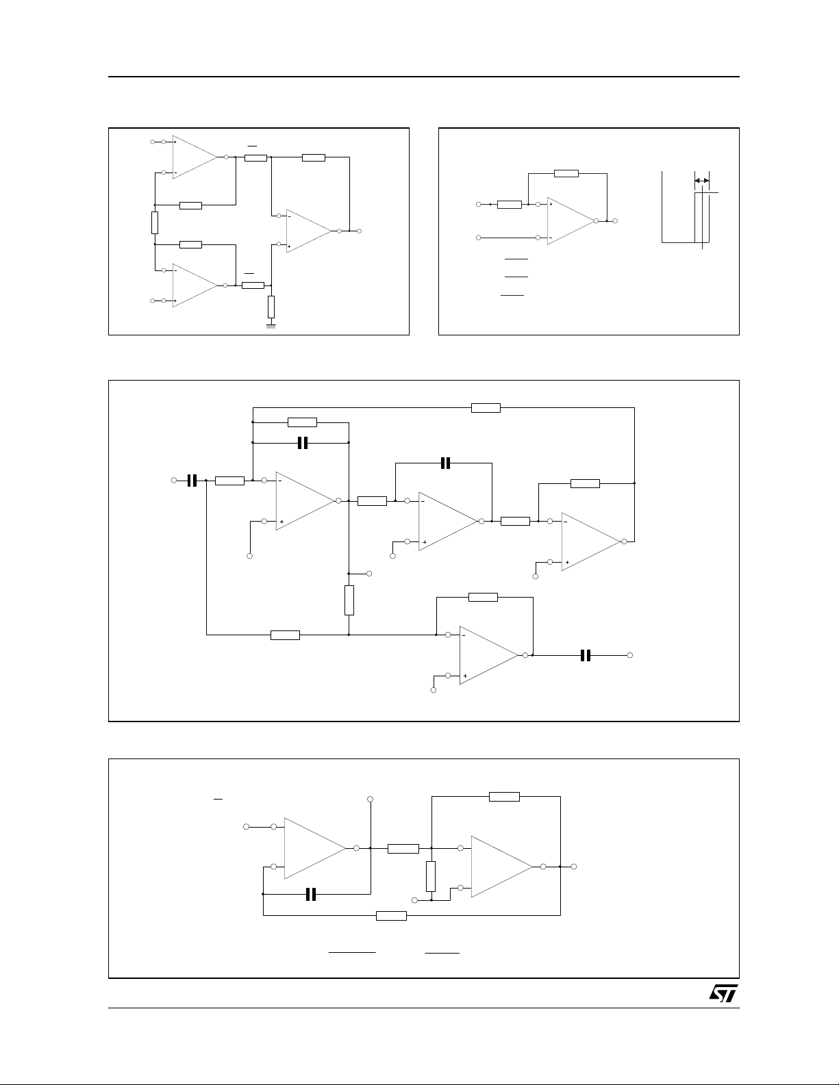
APPLICATION INFORMATION
VOLTAGE REFERENCE
TYPICAL PERFORMANCE CURVES
WIEN BRIDGE OSCILLATOR
20µs/div.
5/10
MC3303 - MC3403 - MC3503
1/4
MC3403
1/4
MC3403
1/4
MC3403
1/4
MC3403
R
R
C
C
R
100k
Ω
100k
Ω
C1
R2
e
I
V
(ref)
R2
R1
Bandpass output
V
(ref)
V
(ref)
R3
V
(ref)
C1
Notch output
R = 160k
Ω
C = 0.001
µ
F
R1 = 1.6M Ω
R2 = 1.6M Ω
R3 = 1.6M Ω
T = Passband notch gain
N
Where T = Center frequency gain
BP
HIGH IMPEDANC E DIFFERENTIAL AMPL IFIER COMPARATOR WITH HYSTERESIS
e
1
R1
e
2
1/4
MC3403
a R1
b R1
1/4
MC3403
BI-QUAD FILTER
1
R
C
1
R
C
R
1/4
MC3403
e
= C (1 + a + b) ( - )
o
R
R2
V
e
o
e
e
2
1
V
R1
(ref)
I
R1
V = [V - V ] + V
IL
R1+R2
R1
V = [V - V ] + V
IH
R1+R2
R1
H = [V - V ]
R1+R2
OH
OL
OL
1/4
MC3403
(ref)
(ref)
OL
V
O
(ref)
(ref)
Hysteresis
V
OH
V
O
V
OL
V
V
IL
IH
V
(ref)
FUNCTION GENERATOR
V
(ref)
1
V
=
CC
2
V
(ref)
1/4
MC3403
C
f =
Triangle wave output
R3
75k
100k
V
(ref)
R
f
R1 + R2
4 CR R1
if R3 =
f
Ω
R1
Ω
R2 R1
R2 + R1
6/10
R2
300k
1/4
MC3403
Ω
Square wave output
MULTIPLE FEEDBACK BANDPASS FILTER
MC3303 - MC3403 - MC3503
C
R1
e
I
R3
C
V
CC
1/4
MC3403
R2
V
(ref)
Given f = center frequency ; chosse valuesf,Cthan
o o
A (f ) = gain at center frequency
o
V
(ref)
For less than 10% error from operational amplifier
QF
oo
< 0.1 where f and BW are expressed in Hz
BW
o
If source impedance varies, filter may be preceded with voltage
follower buffer to stabilize filter parameters
TYPICAL PERFORMANCE CURVES
e
o
C
O
= 10C
C
O
1
V
=
CC
2
R3 =
R1 =
R2 =
Q
fCp
o
R3
2A (f )
o
R1 R5
2
4Q R1-R5
7/10
MC3303 - MC3403 - MC3503
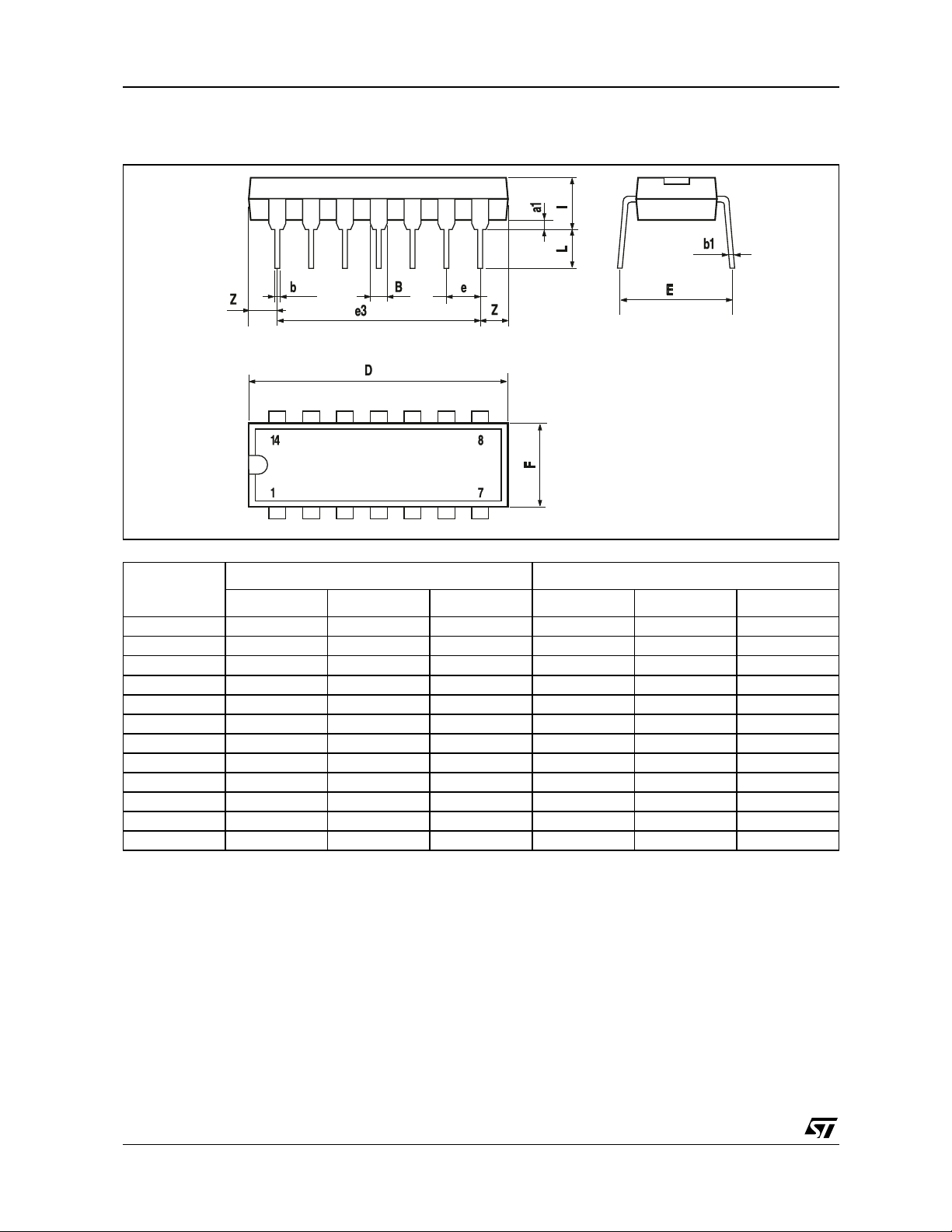
PACKAGE MECHANICAL DATA
14 PINS - PLASTIC PACKAGE
Dimensions
Min. Typ. Max. Min. Typ. Max.
a1 0.51 0.020
B 1.39 1.65 0.055 0.065
b 0.5 0.020
b1 0.25 0.010
D 20 0.787
E 8.5 0.335
e 2.54 0.100
e3 15.24 0.600
F 7.1 0.280
i 5.1 0.201
L 3.3 0.130
Z 1.27 2.54 0.050 0.100
Millimeters Inches
8/10

PACKAGE MECHANICAL DATA
14 PINS - PLASTIC MICROPACKAGE (SO)
a2
LG
A
MC3303 - MC3403 - MC3503
C
c1
b
e3
D
14
e
s
a1
b1
E
M
8
F
1
Millimeters Inches
Dimensions
Min. Typ. Max. Min. Typ. Max.
A 1.75 0.069
a1 0.1 0.2 0.004 0.008
a2 1.6 0.063
b 0.35 0.46 0.014 0.018
b1 0.19 0.25 0.007 0.010
C 0.5 0.020
c1 45° (typ.)
D (1) 8.55 8.75 0.336 0.344
E 5.8 6.2 0.228 0.244
e 1.27 0.050
e3 7.62 0.300
F (1) 3.8 4.0 0.150 0.157
G 4.6 5.3 0.181 0.208
L 0.5 1.27 0.020 0.050
M 0.68 0.027
S 8° (max.)
Note : (1) D and F do not include mold flash or protrusions - Mold flash or protrusions shall not exceed 0.15mm (.066 inc) ONLY FOR DATA BOOK.
7
9/10

MC3303 - MC3403 - MC3503
PACKAGE MECHANICAL DATA
14 PINS - THIN SHRINK SMALL OUT L INE PAC KAG E
c
E1
A
A2
A1
b
D
C
aaa
0,25 mm
.010 inch
GAGE PLANE
PLANE
SEATING
14
PIN 1 IDENTIFICATION
k
L
L1
C
E
e
78
1
Millimeters Inches
Dimensions
Min. Typ. Max. Min. Typ. Max.
A 1.20 0.05
A1 0.05 0.15 0.01 0.006
A2 0.80 1.00 1.05 0.031 0.039 0.041
b 0.19 0.30 0.007 0.15
c 0.09 0.20 0.003 0.012
D 4.90 5.00 5.10 0.192 0.196 0.20
E 6.40 0.252
E1 4.30 4.40 4.50 0.169 0.173 0.177
e 0.65 0.025
k 0° 8° 0° 8°
L 0.450 0.600 0.750 0.018 0.024 0.030
L1 1.00 0.039
aaa 0.100 0.004
Information furnished is bel ieved to be accurate and reliable. However, STMicroe lectronics assumes no responsibility for the
consequences of use of such information nor for any infringement of patents or other rights of third parties which may result from
its use. No li cense is granted by implica tion or otherwise under any patent or patent righ ts of S TMic roelec tronics. Specifications
mentioned in this publication ar e subject to change without notice. This publication supersedes and replaces all information
previously supplied. S TMicroelectronics products are not authorized for use as critica l components in life suppo rt devices or
systems without express written approval of STMicroelectronics.
© The ST logo is a registered trademark of STMicroelectronics
© 2001 STM icroelectronics - Prin ted in Italy - All Rights Reserved
STMicr o el ectronics GROU P OF COMPANIE S
Australi a - Brazil - Canada - China - Fi nl and - France - Germany - Hon g Kong - India - Israel - Italy - Japan - Malaysi a
Malta - Mor occo - Singap ore - Spain - Sweden - Switzerl and - United K i ngdom - United S tates
© http://www.st.com
10/10
 Loading...