

ST MC1489, MC1489A User Manual

MC1489
MC1489A
QUAD LINE RECEIVERS
■INPUT RESISTANCE –3k to 7kΩ
■INPUT SIGNAL RANGE – ± 30V
■INPUT THRESHOLD HYSTERESIS BUILT-IN
■RESPONSE CONTROL:
a) LOGIC THRESHOLD SHIFTING b) INPUT NOISE FILTERING
DESCRIPTION |
|
|
The MC1489 monolithic quad line receivers are |
DIP |
|
designed to interface data terminal equipment |
||
|
||
with data communications equipment in |
|
|
conformance with the specifications of EIA |
|
|
Standard N° RS232C. |
|
SOP
SCHEMATIC DIAGRAM
September 2003 |
1/13 |
MC1489/MC1489A
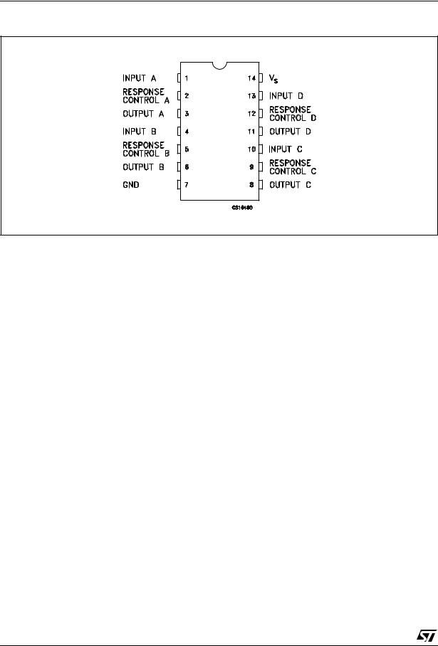
PIN CONFIGURATION (top view)
ORDERING CODES
|
DIP14 |
|
SO14 |
SO14 (TAPE & REEL) |
|
|
|
|
|
|
|
|
|
|
MC1489P |
|
MC1489D1 |
MC1489D1013TR |
|
|
|
|
|
|
|
|
|
|
MC1489AP |
|
|
MC1489AD1013TR |
|
|
|
|
|
|
|
|
|
ABSOLUTE MAXIMUM RATINGS |
|
|
|
|
||
|
|
|
|
|
|
|
Symbol |
|
Parameter |
|
Value |
|
Unit |
|
|
|
|
|
|
|
VS |
Power Supply Voltage |
|
10 |
|
V |
|
VI |
Input Voltage Range |
|
±30 |
|
V |
|
IOL |
Output Load Current |
|
20 |
|
mA |
|
PTOT |
Power Dissipation |
|
1 |
|
W |
|
Tamb |
Operating Ambient Temperature |
|
0 to 75 |
|
°C |
|
Tstg |
Storage Temperature Range |
|
-65 to 150 |
|
°C |
|
Absolute Maximum Ratings are those values beyond which damage to the device may occur. Functional operation under these condition is not implied.
2/13
MC1489/MC1489A
ELECTRICAL CHARACTERISTICS
Response Control Pin in Open; VS = 5V, Tamb = 0 to 75°C, unless otherwise specified.
Symbol |
Parameter |
|
Test Conditions |
Min. |
Typ. |
Max. |
Unit |
|||
|
|
|
|
|
|
|
|
|
|
|
IIH |
Positive Input Current |
VIH = 25 V |
|
|
3.6 |
|
|
8.3 |
mA |
|
|
|
VIH = 3 V |
|
|
0.43 |
|
|
|
|
|
IIL |
Negative Input Current |
VIL = - 25 V |
|
|
-3.6 |
|
|
-8.3 |
mA |
|
|
|
VIL = - 3 V |
|
|
-0.43 |
|
|
|
|
|
VIH |
Input Turn-On Threshold |
Tamb = 25°C, V OL £ 0.45 V |
for MC1489 |
1 |
|
|
1.5 |
V |
||
|
Voltage |
IL = 10 mA |
for MC1489A |
1.75 |
|
1.95 |
2.25 |
|
||
|
|
|
|
|||||||
VIL |
Input Turn-Off Threshold |
Tamb = 25°C, V OL ³ 2.5 V IL = |
-0.5 mA |
0.75 |
|
|
1.25 |
V |
||
|
Voltage |
|
|
|
|
|
|
|
|
|
VOH |
Output Voltage High |
VIH = 0.75 V, IL = -0.5 mA |
|
|
2.5 |
|
4 |
5 |
V |
|
|
|
IL = 0.5 mA Input Open Circuit |
2.5 |
|
4 |
5 |
|
|||
VOL |
Output Voltage Low |
VIL = 3 V, IL = 10 mA |
|
|
|
|
0.2 |
0.45 |
V |
|
IOS |
Output Short Circuit |
|
|
|
|
|
|
-3 |
-4 |
mA |
|
Current |
|
|
|
|
|
|
|
|
|
IS |
Power Supply Current |
All gates "ON", IO = 0 mA, VIH = 5 V |
|
|
16 |
26 |
mA |
|||
PC |
Power Consumption |
VIH = 5 V |
|
|
|
|
80 |
130 |
mW |
|
SWITCHING CHARACTERISTICS |
|
|
|
|
|
|
|
|||
VS = 5V, Tamb = 25°C, (see Figure 1) |
|
|
|
|
|
|
|
|||
Symbol |
Parameter |
|
Test Conditions |
|
Min. |
|
Typ. |
Max. |
Unit |
|
|
|
|
|
|
|
|
|
|
|
|
tPLH |
Propagation Delay Time |
|
RL = 3.9 KΩ |
|
|
|
|
25 |
85 |
ns |
tTHL |
Rise Time |
|
RL = 3.9 KΩ |
|
|
|
|
120 |
175 |
ns |
tPHL |
Propagation Delay Time |
|
RL = 390 Ω |
|
|
|
|
25 |
50 |
ns |
tTHL |
Fall Time |
|
RL = 390 Ω |
|
|
|
|
10 |
20 |
ns |
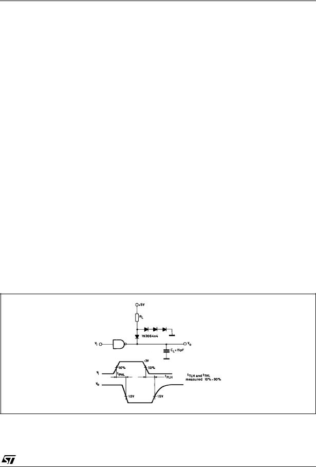
TEST CIRCUITS
Figure 1 : Switching Response
3/13
MC1489/MC1489A
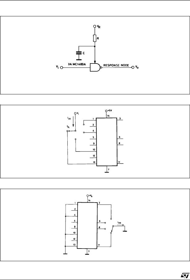
Figure 2 : Response Control Node
C: capacitor is for noise filtering
Figure 3 : Input Current
Figure 4 : Output Short-Circuit Current
4/13
 Loading...