


■ INPUT RESISTANCE –3kto 7kΩ
■ INPUT SIGNAL RANGE – ± 30V
■ INPUT THRESHOLD HYSTERESIS BUILT-IN
■ RESPONSE CON TROL:
a) LOGIC T HRE SHOLD SHIFTING
b) INPUT NOISE FILTERING
DESCRIPTION
The MC1489 monolithic quad line receivers are
designed to interface data terminal equipment
with data communications equipment in
conformance with the specifications of EIA
Standard N° RS232C.
MC1489
MC1489A
QUAD LINE RECEIVERS
DIP
SCHEMATIC DIAGRAM
SOP
1/13September 2003

MC1489/MC1489A
PIN CONFIGURATION (top view)
ORDERING CODES
DIP14 SO14 SO14 (TAPE & REEL)
MC1489P MC1489D1 MC1489D1013TR
MC1489AP MC1489AD1013TR
ABSOLUTE MAXIMUM RATINGS
Symbol Parameter Value Unit
V
V
I
OL
P
TOT
T
amb
T
Absolute Maximum Ratings are those values beyond which damage to the device may occur. Functional operation under these condition is
not implied.
Power Supply Voltage
S
Input Voltage Range
I
Output Load Current
Power Dissipation
Operating Ambient Temperature
Storage Temperature Range
stg
10 V
±30 V
20 mA
1W
0to75 °C
-65 to 150 °C
2/13

MC1489/MC1489A
ELECTRICAL CHARACTERISTICS
Response Control Pin in Open; V
Symbol Parameter Test Conditions Min. Typ. Max. Unit
I
Positive Input Current VIH=25V 3.6 8.3 mA
IH
Negative Input Current VIL= - 25 V -3.6 -8.3 mA
I
IL
Input Turn-On Threshold
V
IH
Voltage
Input Turn-Off Threshold
V
IL
Voltage
V
V
Output Voltage High VIH=0.75V,IL=-0.5mA 2.5 4 5 V
OH
Output Voltage Low VIL=3V, IL= 10 mA 0.2 0.45 V
OL
Output Short Circuit
I
OS
Current
I
Power Supply Current All gates "ON", IO=0mA,VIH= 5 V 16 26 mA
S
Power Consumption VIH= 5 V 80 130 mW
P
C
SWITCHING CHARACTERISTICS
=5V,T
V
S
Symbol Parameter Test Conditions Min. Typ. Max. Unit
t
PLH
t
THL
t
PHL
t
THL
= 25°C, (see Figure 1)
amb
Propagation Delay Time RL= 3.9 KΩ 25 85 ns
Rise Time RL= 3.9 KΩ 120 175 ns
Propagation Delay Time RL=390Ω 25 50 ns
Fall Time RL=390Ω 10 20 ns
=5V,T
S
= 3 V 0.43
V
IH
= - 3 V -0.43
V
IL
T
= 25°C, V
amb
I
=10mA
L
T
= 25°C, V
amb
= 0.5 mA Input Open Circuit 2.5 4 5
I
L
= 0 t o 75°C, unless otherwise spec if ied.
amb
≤ 0.45 V
OL
for MC1489 1 1.5 V
for MC1489A 1.75 1.95 2.25
≥ 2.5VI
OL
=-0.5mA
L
0.75 1.25 V
-3 -4 mA
TEST CIRCUITS
Figure1 : Switching Response
3/13

MC1489/MC1489A
Figure2 : Response Control Node
Figure3 : Input Current
C: capacitor is for noise filtering
Figure4 : Output Short-Circuit Current
4/13

Figure5 : Output Voltage and Input Thres hold Voltage
Figure6 : Power Supply Currents
MC1489/MC1489A
5/13

MC1489/MC1489A
TYPICAL APPLICATIONS:
Figure7 : RS232C Data Transmission
TYPICAL CHARACTERISTICS V
=5V,T
S
= 25°C, unl es s otherwise specified
amb
Figure8 : Input Current v s Input Voltage Figure 9 : MC1489 I nput Threshold Voltage
Adjustment
6/13
MC1489/MC1489A
Figure10 : MC1489A Input Threshold Voltage
Adjustment
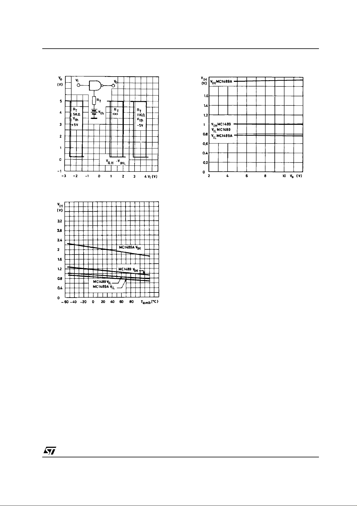
Figure11 : Input Threshold vs Temperature
Figure12 : Input Threshold vs Power Supply
Voltage
7/13

MC1489/MC1489A
APPLICATION INFORMATION
The Electronic Industries Association (EIA) has released the RS-232C specification detailing the
requirements for the interface between data processing equipment and data communications equipment.
This standard specifies not only the number and type of interface leads, but also the voltage levels to be
used. The MC1488 quad driver and its companion circuit, the MC1489 qua d receiver, provide a complete
interface system between DTL or TTL logic levels and the RS-232C defined levels. The RS-232C
requirements as applied to receivers are discussed herein.
The required input impedance is defined as between 3000Ω and 7000Ω for input voltages between 3.0
and 25V in magnitude; and any voltage on the receiver input inan open circuit condition must be less than
2.0V in magnitude. The MC1489 circuits meet these requirements with a maximum open circuit voltage of
one V
The receiver shall detect a voltage between - 3.0 and - 25V as a Logic "1" and inputs between + 3.0 and
+ 2 .5V as a Lo gic "0". On s ome interchange leads, an open circuit of power "OFF" condition (300Ω or
more to ground) shall be decoded as an "OFF" condition or Logic "1". For the reason, the input hysteresis
thresholds of the MC1489 circuits are al l above ground. Thus an open or grounde d input will cause the
same output as a negative or Logic "1" input .
DEVICE CHARACTERISTICS
The MC1489 interface receivers have internal feedback from the second stage to the input stage
providing input hysteresis for noise rejection. The MC1489 input has typical turn-on voltage of 1.25V and
turn-off of1.0 V for a typical hysteresis of 250mV. The MC1489A has t y pical turn-on of 1.95V and turn-off
of 0.8V for typically 1.15V of hysteresis.
Each receiver section has an external response control node in addition to the input and output pins,
thereby allowing the designer to vary the input threshold voltage levels. A resistor can be connected
between this node and an external power supply. Figures 2, 4 and 5 illustrate the input threshold voltage
shift possible through this technique.
This response node can also be used for the filtering of the high-frequency, high-energy noise pulses.
Figures 9 and 10 show typical noise-pulse rej ec tion for external capacitors of various sizes.
These two operations on the response node can be combined or used individually for may combinations
of interfacing applications. The MC1489 circuits are particularly useful for interfacing between MOS
circuits and MDTL/MTTL logic systems. I n thisapplication, the input threshold voltages areadjusted. (with
the appropriate supply and resistor values) to fall in the center of the MOS voltage logic levels (see Figure
11).
The response node may also be used as the receiver input as long as the designer realizes that he may
not drivethis node with a low impedance source to a voltage greater than one diode above ground or less
than one diode below ground. This feature is demonstrated in Figure 12 where two receivers are slaved
to the s ame line that must still meet the RS-232C impedance requirement.
BE
.
Figure13 : Typical T urn-on Threshold vs
Capacitance from Response Control Pin to GND
8/13
Figure14 : Typical T urn-on Threshold vs
Capacitance from Response Control Pin to GND

Figure15 : Typical Paralleling of Two MC1489/A Receivers to M eet RS-232C
MC1489/MC1489A
9/13

MC1489/MC1489A
Plastic DIP-14 MECHANICAL DATA
mm. inch
DIM.
MIN. TYP MAX. MIN. TYP. MAX.
a1 0.51 0.020
B 1.39 1.65 0.055 0.065
b 0.5 0.020
b1 0.25 0.010
D 20 0.787
E 8.5 0.335
e 2.54 0.100
e3 15.24 0.600
F 7.1 0.280
I 5.1 0.201
L 3.3 0.130
Z 1.27 2.54 0.050 0.100
10/13
P001A

SO-14 MECHANICAL DATA
MC1489/MC1489A
DIM.
A 1.75 0.068
a1 0.1 0.2 0.003 0.007
a2 1.65 0.064
b 0.35 0.46 0.013 0.018
b1 0.19 0.25 0.007 0.010
C 0.5 0.019
c1 45˚ (typ.)
D 8.55 8.75 0.336 0.344
E 5.8 6.2 0.228 0.244
e 1.27 0.050
e3 7.62 0.300
F 3.8 4.0 0.149 0.157
G 4.6 5.3 0.181 0. 208
L 0.5 1.27 0.019 0.050
M 0.68 0.026
S ˚ (max.)
MIN. TYP MAX. MIN. TYP. MAX.
mm. inch
8
PO13G
11/13

MC1489/MC1489A
Tape & Reel SO-14 MECHANICAL DATA
mm. inch
DIM.
MIN. TYP MAX. MIN. TYP. MAX.
A 330 12.992
C 12.8 13.2 0.504 0.519
D 20.2 0.795
N 60 2.362
T 22.4 0.882
Ao 6.4 6.6 0.252 0.260
Bo 9 9.2 0.354 0.362
Ko 2.1 2.3 0.082 0.090
Po 3.9 4.1 0.153 0.161
P 7.9 8.1 0.311 0.319
12/13

MC1489/MC1489A
Information furnished is believed to be accurate and reliable. However, STMicroelectronics assumes no responsibility for the
consequences of use o f suc h info rmat ion n or for any in fring ement of paten ts or oth er ri ghts of th ird p arties which may resul t f rom
its use. No license is granted by implication or otherwise under any patent or patent rights of STMicroelectronics. Specifications
mentioned in this publication are subject to change without notice. This publication supersedes and replaces all information
previously supplied. STMicroelectronics products are not authorized for use as critical components in life support devices or
systems without express written approval of STMicroelectronics.
Australia - Belgium - Brazil - Canada - China - Czech Republic - Finland - France - Germany - Hong Kong - India - Israel - Italy - Japan -
Malaysia - Malta - Morocco - Singapore - Spain - Sweden - Switzerland - United Kingdom - United States.
The ST logo is a registered trademark of STMicroelectronics
All other names are the property of their respective owners
© 2003 STMicroelectronics - All Rights Reserved
STMicroelectronics GROUP OF COMPANIES
http://www.st.com
13/13
 Loading...