

ST M95640, M95640-W, M95640-R, M95640-DR User Manual
M95640 M95640-W M95640-R
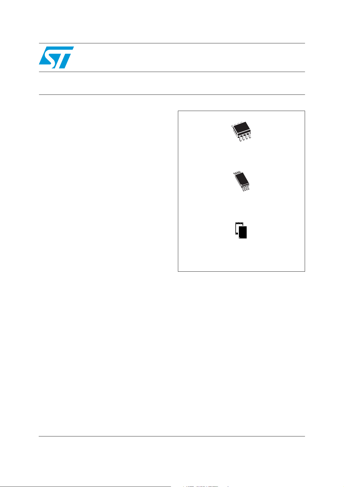
UFDFPN8 (MB or MC)
2 x 3 mm
TSSOP8 (DW)
169 mil width
SO8 (MN)
150 mil width
Features
■ Compatible with the Serial Peripheral Interface
(SPI) bus
■ Memory array
– 64 Kb (8 Kbytes) of EEPROM
– Page size: 32 bytes
■ Additional Write lockable Page (Identification
page)
■ Write (self timed cycle)
– Byte Write within 5 ms
– Page Write within 5 ms
■ Write Protect: quarter, half or whole memory
array
■ High speed clock frequency (20 MHz)
■ Single supply voltage: 1.8 V to 5.5 V
■ More than 1 million Write cycles
■ More than 40-year data retention
■ Enhanced ESD Protection
■ Packages
–ECOPACK2
Halogen-free)
®
(RoHS-compliant and
M95640-DR
64 Kbit serial SPI bus EEPROMs
with high-speed clock
April 2011 Doc ID 16877 Rev 15 1/48
www.st.com
1

Contents M95640, M95640-W, M95640-R, M95640-DR
Contents
1 Description . . . . . . . . . . . . . . . . . . . . . . . . . . . . . . . . . . . . . . . . . . . . . . . . . 6
2 Signal description . . . . . . . . . . . . . . . . . . . . . . . . . . . . . . . . . . . . . . . . . . . 8
2.1 Serial Data output (Q) . . . . . . . . . . . . . . . . . . . . . . . . . . . . . . . . . . . . . . . . 8
2.2 Serial Data input (D) . . . . . . . . . . . . . . . . . . . . . . . . . . . . . . . . . . . . . . . . . . 8
2.3 Serial Clock (C) . . . . . . . . . . . . . . . . . . . . . . . . . . . . . . . . . . . . . . . . . . . . . 8
2.4 Chip Select (S
2.5 Hold (HOLD
2.6 Write Protect (W
2.7 V
2.8 V
ground . . . . . . . . . . . . . . . . . . . . . . . . . . . . . . . . . . . . . . . . . . . . . . . . . 9
SS
supply voltage . . . . . . . . . . . . . . . . . . . . . . . . . . . . . . . . . . . . . . . . . . . 9
CC
) . . . . . . . . . . . . . . . . . . . . . . . . . . . . . . . . . . . . . . . . . . . . . . 8
) . . . . . . . . . . . . . . . . . . . . . . . . . . . . . . . . . . . . . . . . . . . . . . . . 8
) . . . . . . . . . . . . . . . . . . . . . . . . . . . . . . . . . . . . . . . . . . . . 9
3 Connecting to the SPI bus . . . . . . . . . . . . . . . . . . . . . . . . . . . . . . . . . . . 10
3.1 SPI modes . . . . . . . . . . . . . . . . . . . . . . . . . . . . . . . . . . . . . . . . . . . . . . . . 11
4 Operating features . . . . . . . . . . . . . . . . . . . . . . . . . . . . . . . . . . . . . . . . . 12
4.1 Supply voltage (VCC) . . . . . . . . . . . . . . . . . . . . . . . . . . . . . . . . . . . . . . . . 12
4.1.1 Operating supply voltage V
4.1.2 Device reset . . . . . . . . . . . . . . . . . . . . . . . . . . . . . . . . . . . . . . . . . . . . . . 12
4.1.3 Power-up conditions . . . . . . . . . . . . . . . . . . . . . . . . . . . . . . . . . . . . . . . 12
4.1.4 Power-down . . . . . . . . . . . . . . . . . . . . . . . . . . . . . . . . . . . . . . . . . . . . . . 13
4.2 Active Power and Standby Power modes . . . . . . . . . . . . . . . . . . . . . . . . . 13
4.2.1 Hold condition . . . . . . . . . . . . . . . . . . . . . . . . . . . . . . . . . . . . . . . . . . . . 13
CC . . . . . . . . . . . . . . . . . . . . . . . . . . . . . . . . . . . . . . . . . 12
4.3 Status Register . . . . . . . . . . . . . . . . . . . . . . . . . . . . . . . . . . . . . . . . . . . . . 14
4.4 Data protection and protocol control . . . . . . . . . . . . . . . . . . . . . . . . . . . . 14
5 Memory organization . . . . . . . . . . . . . . . . . . . . . . . . . . . . . . . . . . . . . . . 15
6 Instructions . . . . . . . . . . . . . . . . . . . . . . . . . . . . . . . . . . . . . . . . . . . . . . . 16
6.1 Write Enable (WREN) . . . . . . . . . . . . . . . . . . . . . . . . . . . . . . . . . . . . . . . 16
6.2 Write Disable (WRDI) . . . . . . . . . . . . . . . . . . . . . . . . . . . . . . . . . . . . . . . . 18
6.3 Read Status Register (RDSR) . . . . . . . . . . . . . . . . . . . . . . . . . . . . . . . . . 19
6.3.1 WIP bit . . . . . . . . . . . . . . . . . . . . . . . . . . . . . . . . . . . . . . . . . . . . . . . . . . 19
2/48 Doc ID 16877 Rev 15

M95640, M95640-W, M95640-R, M95640-DR Contents
6.3.2 WEL bit . . . . . . . . . . . . . . . . . . . . . . . . . . . . . . . . . . . . . . . . . . . . . . . . . 19
6.3.3 BP1, BP0 bits . . . . . . . . . . . . . . . . . . . . . . . . . . . . . . . . . . . . . . . . . . . . . 19
6.3.4 SRWD bit . . . . . . . . . . . . . . . . . . . . . . . . . . . . . . . . . . . . . . . . . . . . . . . . 19
6.4 Write Status Register (WRSR) . . . . . . . . . . . . . . . . . . . . . . . . . . . . . . . . . 20
6.5 Read from Memory Array (READ) . . . . . . . . . . . . . . . . . . . . . . . . . . . . . . 22
6.6 Write to Memory Array (WRITE) . . . . . . . . . . . . . . . . . . . . . . . . . . . . . . . 23
6.7 Read Identification Page . . . . . . . . . . . . . . . . . . . . . . . . . . . . . . . . . . . . . 24
6.8 Write Identification Page . . . . . . . . . . . . . . . . . . . . . . . . . . . . . . . . . . . . . 26
6.9 Read Lock Status . . . . . . . . . . . . . . . . . . . . . . . . . . . . . . . . . . . . . . . . . . . 26
6.10 Lock ID . . . . . . . . . . . . . . . . . . . . . . . . . . . . . . . . . . . . . . . . . . . . . . . . . . . 27
7 Power-up and delivery state . . . . . . . . . . . . . . . . . . . . . . . . . . . . . . . . . . 28
7.1 Power-up state . . . . . . . . . . . . . . . . . . . . . . . . . . . . . . . . . . . . . . . . . . . . . 28
7.2 Initial delivery state . . . . . . . . . . . . . . . . . . . . . . . . . . . . . . . . . . . . . . . . . . 28
8 Maximum rating . . . . . . . . . . . . . . . . . . . . . . . . . . . . . . . . . . . . . . . . . . . . 29
9 DC and AC parameters . . . . . . . . . . . . . . . . . . . . . . . . . . . . . . . . . . . . . . 30
10 Package mechanical data . . . . . . . . . . . . . . . . . . . . . . . . . . . . . . . . . . . . 40
11 Part numbering . . . . . . . . . . . . . . . . . . . . . . . . . . . . . . . . . . . . . . . . . . . . 43
12 Revision history . . . . . . . . . . . . . . . . . . . . . . . . . . . . . . . . . . . . . . . . . . . 44
Doc ID 16877 Rev 15 3/48

List of tables M95640, M95640-W, M95640-R, M95640-DR
List of tables
Table 1. Signal names . . . . . . . . . . . . . . . . . . . . . . . . . . . . . . . . . . . . . . . . . . . . . . . . . . . . . . . . . . . . 7
Table 2. Write-protected block size . . . . . . . . . . . . . . . . . . . . . . . . . . . . . . . . . . . . . . . . . . . . . . . . . 14
Table 3. M95640-x Instruction set . . . . . . . . . . . . . . . . . . . . . . . . . . . . . . . . . . . . . . . . . . . . . . . . . . 16
Table 4. M95640-DR instruction set . . . . . . . . . . . . . . . . . . . . . . . . . . . . . . . . . . . . . . . . . . . . . . . . . 16
Table 5. Status Register format . . . . . . . . . . . . . . . . . . . . . . . . . . . . . . . . . . . . . . . . . . . . . . . . . . . . 19
Table 6. Protection modes . . . . . . . . . . . . . . . . . . . . . . . . . . . . . . . . . . . . . . . . . . . . . . . . . . . . . . . . 21
Table 7. Address range bits . . . . . . . . . . . . . . . . . . . . . . . . . . . . . . . . . . . . . . . . . . . . . . . . . . . . . . . 21
Table 8. Absolute maximum ratings . . . . . . . . . . . . . . . . . . . . . . . . . . . . . . . . . . . . . . . . . . . . . . . . . 29
Table 9. Operating conditions (M95640 device grade 3) . . . . . . . . . . . . . . . . . . . . . . . . . . . . . . . . . 30
Table 10. Operating conditions (M95640-W) . . . . . . . . . . . . . . . . . . . . . . . . . . . . . . . . . . . . . . . . . . . 30
Table 11. Operating conditions (M95640-R device grade 6) . . . . . . . . . . . . . . . . . . . . . . . . . . . . . . . 30
Table 12. AC measurement conditions. . . . . . . . . . . . . . . . . . . . . . . . . . . . . . . . . . . . . . . . . . . . . . . . 30
Table 13. Capacitance . . . . . . . . . . . . . . . . . . . . . . . . . . . . . . . . . . . . . . . . . . . . . . . . . . . . . . . . . . . . 31
Table 14. DC characteristics (M95640, device grade 3). . . . . . . . . . . . . . . . . . . . . . . . . . . . . . . . . . . 31
Table 15. DC characteristics (M95640-W, device grade 6) . . . . . . . . . . . . . . . . . . . . . . . . . . . . . . . . 32
Table 16. DC characteristics (M95640-W, device grade 3) . . . . . . . . . . . . . . . . . . . . . . . . . . . . . . . . 33
Table 17. DC characteristics (M95640-R, M95640-DR, device grade 6) . . . . . . . . . . . . . . . . . . . . . . 33
Table 18. AC characteristics (M95640, device grade 3) . . . . . . . . . . . . . . . . . . . . . . . . . . . . . . . . . . . 34
Table 19. AC characteristics (M95640-W products, device grade 6) . . . . . . . . . . . . . . . . . . . . . . . . . 35
Table 20. AC characteristics (M95640-W products, device grade 3) . . . . . . . . . . . . . . . . . . . . . . . . . 36
Table 21. AC characteristics (M95640-R, M95640-DR devices, grade 6) . . . . . . . . . . . . . . . . . . . . . 37
Table 22. SO8N – 8-lead plastic small outline, 150 mils body width, package mechanical data . . . . 40
Table 23. TSSOP8 – 8-lead thin shrink small outline, package mechanical data. . . . . . . . . . . . . . . . 41
Table 24. UFDFPN8 (MLP8) 8-lead ultra thin fine pitch dual flat package no lead
2 x 3 mm, data . . . . . . . . . . . . . . . . . . . . . . . . . . . . . . . . . . . . . . . . . . . . . . . . . . . . . . . . . . 42
Table 25. Ordering information scheme . . . . . . . . . . . . . . . . . . . . . . . . . . . . . . . . . . . . . . . . . . . . . . . 43
Table 26. Document revision history . . . . . . . . . . . . . . . . . . . . . . . . . . . . . . . . . . . . . . . . . . . . . . . . . 44
4/48 Doc ID 16877 Rev 15

M95640, M95640-W, M95640-R, M95640-DR List of figures
List of figures
Figure 1. Logic diagram . . . . . . . . . . . . . . . . . . . . . . . . . . . . . . . . . . . . . . . . . . . . . . . . . . . . . . . . . . . . 6
Figure 2. 8-pin package connections . . . . . . . . . . . . . . . . . . . . . . . . . . . . . . . . . . . . . . . . . . . . . . . . . . 6
Figure 3. Bus master and memory devices on the SPI bus . . . . . . . . . . . . . . . . . . . . . . . . . . . . . . . . 10
Figure 4. SPI modes supported . . . . . . . . . . . . . . . . . . . . . . . . . . . . . . . . . . . . . . . . . . . . . . . . . . . . . 11
Figure 5. Hold condition activation . . . . . . . . . . . . . . . . . . . . . . . . . . . . . . . . . . . . . . . . . . . . . . . . . . . 13
Figure 6. Block diagram . . . . . . . . . . . . . . . . . . . . . . . . . . . . . . . . . . . . . . . . . . . . . . . . . . . . . . . . . . . 15
Figure 7. Write Enable (WREN) sequence . . . . . . . . . . . . . . . . . . . . . . . . . . . . . . . . . . . . . . . . . . . . 17
Figure 8. Write Disable (WRDI) sequence . . . . . . . . . . . . . . . . . . . . . . . . . . . . . . . . . . . . . . . . . . . . . 18
Figure 9. Read Status Register (RDSR) sequence . . . . . . . . . . . . . . . . . . . . . . . . . . . . . . . . . . . . . . 20
Figure 10. Write Status Register (WRSR) sequence . . . . . . . . . . . . . . . . . . . . . . . . . . . . . . . . . . . . . . 22
Figure 11. Read from Memory Array (READ) sequence . . . . . . . . . . . . . . . . . . . . . . . . . . . . . . . . . . . 22
Figure 12. Byte Write (WRITE) sequence . . . . . . . . . . . . . . . . . . . . . . . . . . . . . . . . . . . . . . . . . . . . . . 23
Figure 13. Page Write (WRITE) sequence . . . . . . . . . . . . . . . . . . . . . . . . . . . . . . . . . . . . . . . . . . . . . 24
Figure 14. Read Identification Page sequence . . . . . . . . . . . . . . . . . . . . . . . . . . . . . . . . . . . . . . . . . . 25
Figure 15. Write Identification Page sequence . . . . . . . . . . . . . . . . . . . . . . . . . . . . . . . . . . . . . . . . . . 26
Figure 16. Read Lock Status sequence . . . . . . . . . . . . . . . . . . . . . . . . . . . . . . . . . . . . . . . . . . . . . . . . 27
Figure 17. Lock ID sequence . . . . . . . . . . . . . . . . . . . . . . . . . . . . . . . . . . . . . . . . . . . . . . . . . . . . . . . . 27
Figure 18. AC measurement I/O waveform . . . . . . . . . . . . . . . . . . . . . . . . . . . . . . . . . . . . . . . . . . . . . 30
Figure 19. Serial input timing . . . . . . . . . . . . . . . . . . . . . . . . . . . . . . . . . . . . . . . . . . . . . . . . . . . . . . . . 38
Figure 20. Hold timing . . . . . . . . . . . . . . . . . . . . . . . . . . . . . . . . . . . . . . . . . . . . . . . . . . . . . . . . . . . . . 38
Figure 21. Serial output timing . . . . . . . . . . . . . . . . . . . . . . . . . . . . . . . . . . . . . . . . . . . . . . . . . . . . . . . 39
Figure 22. SO8N – 8-lead plastic small outline, 150 mils body width, package outline . . . . . . . . . . . . 40
Figure 23. TSSOP8 – 8-lead thin shrink small outline, package outline . . . . . . . . . . . . . . . . . . . . . . . 41
Figure 24. UFDFPN8 (MLP8) - 8-lead ultra thin fine pitch dual flat no lead, package
outline . . . . . . . . . . . . . . . . . . . . . . . . . . . . . . . . . . . . . . . . . . . . . . . . . . . . . . . . . . . . . . . . . 42
Doc ID 16877 Rev 15 5/48
Description M95640, M95640-W, M95640-R, M95640-DR
AI01789C
S
V
CC
M95xxx
HOLD
V
SS
W
Q
C
D
DV
SS
C
HOLDQ
SV
CC
W
AI01790D
M95xxx
1
2
3
4
8
7
6
5
1 Description
The M95640, M95640-W and M95640-R are electrically erasable programmable memory
(EEPROM) devices. They are accessed by a high-speed SPI-compatible bus. The devices
are 64 Kbit devices organized as 8192 × 8 bits.
The M95640-D also offers an additional page, named the Identification Page (32 bytes)
which can be written and (later) permanently locked in Read-only mode. This Identification
Page offers flexibility in the application board production line, as it can be used to store
unique identification parameters and/or parameters specific to the production line.
The device is accessed by a simple serial interface that is SPI-compatible. The bus signals
are C, D and Q, as shown in Ta bl e 1 and Figure 1.
The device is selected when Chip Select (S
can be interrupted using Hold (HOLD
).
Figure 1. Logic diagram
Figure 2. 8-pin package connections
) is taken low. Communications with the device
1. See Package mechanical data section for package dimensions and how to identify pin-1.
6/48 Doc ID 16877 Rev 15

M95640, M95640-W, M95640-R, M95640-DR Description
Table 1. Signal names
Signal name Description
C Serial Clock
D Serial data input
Q Serial data output
S Chip Select
W
HOLD
Write Protect
Hold
V
CC
V
SS
Supply voltage
Ground
Doc ID 16877 Rev 15 7/48

Signal description M95640, M95640-W, M95640-R, M95640-DR
2 Signal description
During all operations, VCC must be held stable and within the specified valid range:
V
(min) to VCC(max).
CC
All of the input and output signals must be held high or low (according to voltages of V
V
, VIL or VOL, as specified in Ta bl e 1 4 ). These signals are described next.
OH
2.1 Serial Data output (Q)
This output signal is used to transfer data serially out of the device. Data is shifted out on the
falling edge of Serial Clock (C).
2.2 Serial Data input (D)
This input signal is used to transfer data serially into the device. It receives instructions,
addresses, and the data to be written. Values are latched on the rising edge of Serial Clock
(C).
,
IH
2.3 Serial Clock (C)
This input signal provides the timing of the serial interface. Instructions, addresses, or data
present at Serial Data Input (D) are latched on the rising edge of Serial Clock (C). Data on
Serial Data Output (Q) changes after the falling edge of Serial Clock (C).
2.4 Chip Select (S)
When this input signal is high, the device is deselected and Serial Data output (Q) is at high
impedance. Unless an internal Write cycle is in progress, the device will be in the Standby
Power mode. Driving Chip Select (S
mode.
After Power-up, a falling edge on Chip Select (S
instruction.
2.5 Hold (HOLD)
The Hold (HOLD) signal is used to pause any serial communications with the device without
deselecting the device.
During the Hold condition, the Serial Data output (Q) is high impedance, and Serial Data
input (D) and Serial Clock (C) are Don’t Care.
To start the Hold condition, the device must be selected, with Chip Select (S
) low selects the device, placing it in the Active Power
) is required prior to the start of any
) driven low.
8/48 Doc ID 16877 Rev 15

M95640, M95640-W, M95640-R, M95640-DR Signal description
2.6 Write Protect (W)
The main purpose of this input signal is to freeze the size of the area of memory that is
protected against Write instructions (as specified by the values in the BP1 and BP0 bits of
the Status Register).
This pin must be driven either high or low, and must be stable during all write operations.
2.7 VSS ground
VSS is the reference for the VCC supply voltage.
2.8 VCC supply voltage
Refer to Section 4.1: Supply voltage (VCC) on page 12.
Doc ID 16877 Rev 15 9/48
Connecting to the SPI bus M95640, M95640-W, M95640-R, M95640-DR
AI12836b
SPI bus master
SPI memory
device
SDO
SDI
SCK
CQD
S
SPI memory
device
CQD
S
SPI memory
device
CQD
S
CS3 CS2 CS1
SPI interface with
(CPOL, CPHA) =
(0, 0) or (1, 1)
W
HOLD
W
HOLD
W
HOLD
RRR
V
CC
V
CC
V
CC
V
CC
V
SS
V
SS
V
SS
V
SS
R
3 Connecting to the SPI bus
These devices are fully compatible with the SPI protocol.
All instructions, addresses and input data bytes are shifted in to the device, most significant
bit first. The Serial Data input (D) is sampled on the first rising edge of the Serial Clock (C)
after Chip Select (S
All output data bytes are shifted out of the device, most significant bit first. The Serial Data
output (Q) is latched on the first falling edge of the Serial Clock (C) after the instruction (such
as the Read from Memory Array and Read Status Register instructions) have been clocked
into the device.
Figure 3 shows three devices, connected to an MCU, on a SPI bus. Only one device is
selected at a time, so only one device drives the Serial Data output (Q) line at a time, all the
others being high impedance.
Figure 3. Bus master and memory devices on the SPI bus
) goes low.
1. The Write Protect (W) and Hold (HOLD) signals should be driven, high or low as appropriate.
A pull-up resistor connected on each /S input (represented in Figure 3) ensures that each
device is not selected if the bus master leaves the /S line in the high impedance state.
In applications where the bus master might enter a state where all inputs/outputs SPI bus
10/48 Doc ID 16877 Rev 15
would be in high impedance at the same time (for example, if the bus master is reset during
the transmission of an instruction), the clock line (C) must be connected to an external pull-
down resistor so that, if all inputs/outputs become high impedance, the C line is pulled low
(while the S
same time, and so, that the t
line is pulled high): this will ensure that S and C do not become high at the
requirement is met. The typical value of R is 100 kΩ.
SHCH
M95640, M95640-W, M95640-R, M95640-DR Connecting to the SPI bus
AI01438B
C
MSB
CPHA
D
0
1
CPOL
0
1
Q
C
MSB
3.1 SPI modes
These devices can be driven by a microcontroller with its SPI peripheral running in either of
the two following modes:
● CPOL=0, CPHA=0
● CPOL=1, CPHA=1
For these two modes, input data is latched in on the rising edge of Serial Clock (C), and
output data is available from the falling edge of Serial Clock (C).
The difference between the two modes, as shown in Figure 4, is the clock polarity when the
bus master is in Stand-by mode and not transferring data:
● C remains at 0 for (CPOL=0, CPHA=0)
● C remains at 1 for (CPOL=1, CPHA=1)
Figure 4. SPI modes supported
Doc ID 16877 Rev 15 11/48

Operating features M95640, M95640-W, M95640-R, M95640-DR
4 Operating features
4.1 Supply voltage (VCC)
4.1.1 Operating supply voltage V
Prior to selecting the memory and issuing instructions to it, a valid and stable VCC voltage
within the specified [V
(min), VCC(max)] range must be applied (see Ta bl e 9 andTa bl e 1 0).
CC
This voltage must remain stable and valid until the end of the transmission of the instruction
and, for a Write instruction, until the completion of the internal write cycle (t
secure a stable DC supply voltage, it is recommended to decouple the V
suitable capacitor (usually of the order of 10 nF to 100 nF) close to the V
pins.
4.1.2 Device reset
In order to prevent inadvertent write operations during power-up, a power-on-reset (POR)
circuit is included. At power-up, the device does not respond to any instruction until V
reaches the internal threshold voltage (this threshold is defined in DC characteristics tables
14, 15 and16 as V
When V
● in the Standby Power mode
● deselected (note that, to be executed, an instruction must be preceded by a falling
passes over the POR threshold, the device is reset and in the following state:
CC
edge on Chip Select (S
● Status register values:
– the Write Enable Latch (WEL) bit is reset to 0
– the Write In Progress (WIP) bit is reset to 0
– the SRWD, BP1 and BP0 bits remain unchanged (non-volatile bits).
RES
).
))
CC
). In order to
W
line with a
CC
CC/VSS
package
CC
When V
passes over the POR threshold, the device is reset and enters the Standby
CC
Power mode. The device must not be accessed until V
voltage within the specified [V
(min), VCC(max)] range defined in Ta b le 9 andTa bl e 1 0.
CC
4.1.3 Power-up conditions
When the power supply is turned on, VCC continuously rises from VSS to VCC. During this
time, the Chip Select (S
therefore recommended to connect the S
Figure 3).
In addition, the Chip Select (S
sensitive as well as level-sensitive: after power-up, the device does not become selected
until a falling edge has first been detected on Chip Select (S
(S
) must have been high, prior to going low to start the first operation.
The V
voltage has to rise continuously from 0 V up to the minimum VCC operating voltage
CC
defined in Ta bl e 9 and Ta bl e 1 0 and the rise time must not vary faster than 1 V/µs.
12/48 Doc ID 16877 Rev 15
) line is not allowed to float but should follow the VCC voltage. It is
line to VCC via a suitable pull-up resistor (see
) input offers a built-in safety feature, as the S input is edge-
reaches a valid and stable VCC
CC
). This ensures that Chip Select

M95640, M95640-W, M95640-R, M95640-DR Operating features
AI02029D
HOLD
C
Hold
Condition
Hold
Condition
4.1.4 Power-down
During power-down (continuous decrease in the VCC supply voltage below the minimum
V
operating voltage defined in Ta bl e 9 and Ta bl e 1 0 ), the device must be:
CC
● deselected (Chip Select S should be allowed to follow the voltage applied on V
● in Standby Power mode (there should not be any internal write cycle in progress).
CC
)
4.2 Active Power and Standby Power modes
When Chip Select (S) is low, the device is selected, and in the Active Power mode. The
device consumes I
When Chip Select (S
progress, the device then goes in to the Standby Power mode, and the device consumption
drops to I
CC1
.
4.2.1 Hold condition
The Hold (HOLD) signal is used to pause any serial communications with the device without
resetting the clocking sequence.
During the Hold condition, the Serial Data output (Q) is high impedance, and Serial Data
input (D) and Serial Clock (C) are Don’t Care.
, as specified in Ta bl e 1 4 to Ta bl e 1 8 .
CC
) is high, the device is deselected. If a Write cycle is not currently in
To enter the Hold condition, the device must be selected, with Chip Select (S
) low.
Normally, the device is kept selected, for the whole duration of the Hold condition.
Deselecting the device while it is in the Hold condition, has the effect of resetting the state of
the device, and this mechanism can be used if it is required to reset any processes that had
been in progress.
The Hold condition starts when the Hold (HOLD
) signal is driven low at the same time as
Serial Clock (C) already being low (as shown in Figure 5).
The Hold condition ends when the Hold (HOLD
) signal is driven high at the same time as
Serial Clock (C) already being low.
Figure 5 also shows what happens if the rising and falling edges are not timed to coincide
with Serial Clock (C) being low.
Figure 5. Hold condition activation
Doc ID 16877 Rev 15 13/48

Operating features M95640, M95640-W, M95640-R, M95640-DR
4.3 Status Register
Figure 6 shows the position of the Status Register in the control logic of the device. The
Status Register contains a number of status and control bits that can be read or set (as
appropriate) by specific instructions. See Section 6.3: Read Status Register (RDSR) for a
detailed description of the Status Register bits.
4.4 Data protection and protocol control
Non-volatile memory devices can be used in environments that are particularly noisy, and
within applications that could experience problems if memory bytes are corrupted.
Consequently, the device features the following data protection mechanisms:
● Write and Write Status Register instructions are checked that they consist of a number
of clock pulses that is a multiple of eight, before they are accepted for execution.
● All instructions that modify data must be preceded by a Write Enable (WREN)
instruction to set the Write Enable Latch (WEL) bit. This bit is returned to its reset state
by the following events:
–Power-up
– Write Disable (WRDI) instruction completion
– Write Status Register (WRSR) instruction completion
– Write (WRITE) instruction completion
● The Block Protect (BP1, BP0) bits in the Status Register allow part of the memory to be
configured as read-only.
● The Write Protect (W) signal is used to protect the Block Protect (BP1, BP0) bits of the
Status Register.
For any instruction to be accepted, and executed, Chip Select (S
) must be driven high after
the rising edge of Serial Clock (C) for the last bit of the instruction, and before the next rising
edge of Serial Clock (C).
Two points need to be noted in the previous sentence:
● The ‘last bit of the instruction’ can be the eighth bit of the instruction code, or the eighth
bit of a data byte, depending on the instruction (except for Read Status Register
(RDSR) and Read (READ) instructions).
● The ‘next rising edge of Serial Clock (C)’ might (or might not) be the next bus
transaction for some other device on the SPI bus.
Table 2. Write-protected block size
Status Register bits
Protected block
BP1 BP0 64 Kbit devices
0 0 none none
0 1 Upper quarter 1800h - 1FFFh
1 0 Upper half 1000h - 1FFFh
1 1 Whole memory 0000h - 1FFFh
Array addresses protected
14/48 Doc ID 16877 Rev 15
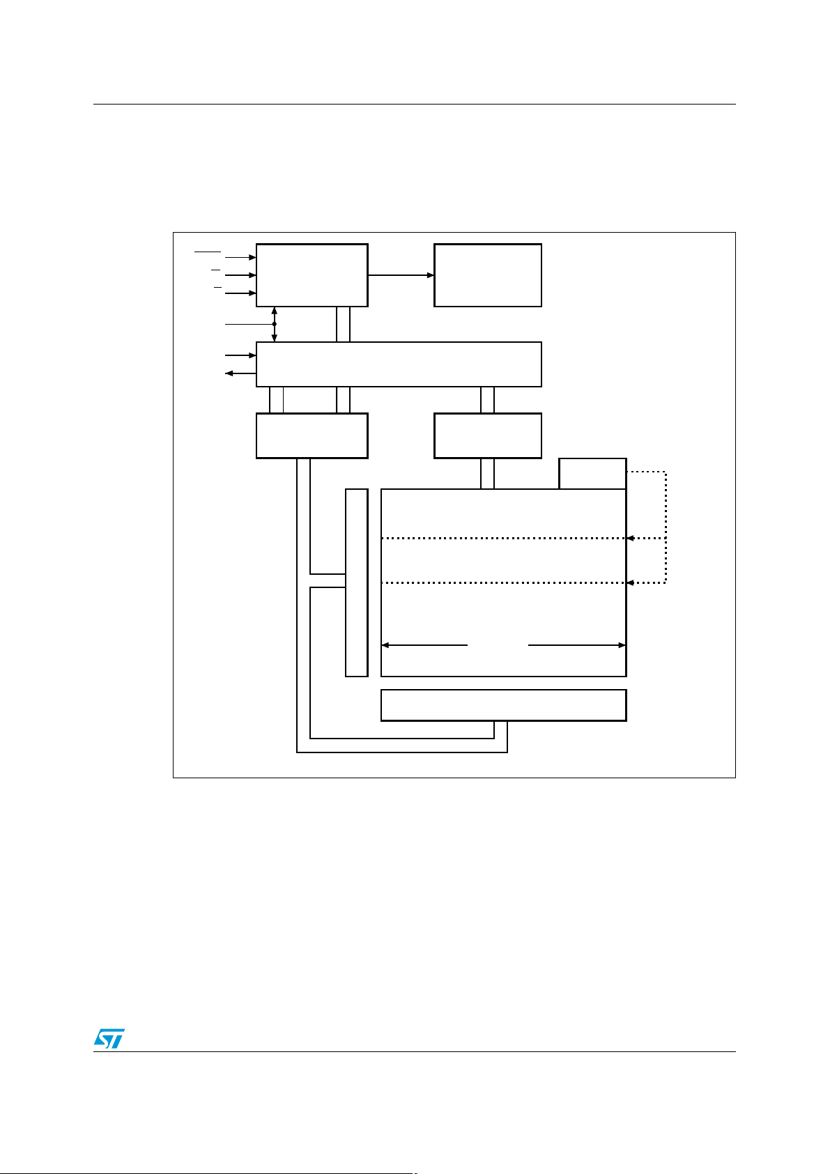
M95640, M95640-W, M95640-R, M95640-DR Memory organization
AI01272C
HOLD
S
W
Control Logic
High Voltage
Generator
I/O Shift Register
Address Register
and Counter
Data
Register
1 Page
X Decoder
Y Decoder
C
D
Q
Size of the
Read only
EEPROM
area
Status
Register
5 Memory organization
The memory is organized as shown in Figure 6.
Figure 6. Block diagram
Doc ID 16877 Rev 15 15/48
 Loading...