

ST M95512-W, M95512-R, M95512-DR, M95512-DF User Manual
M95512-W M95512-R
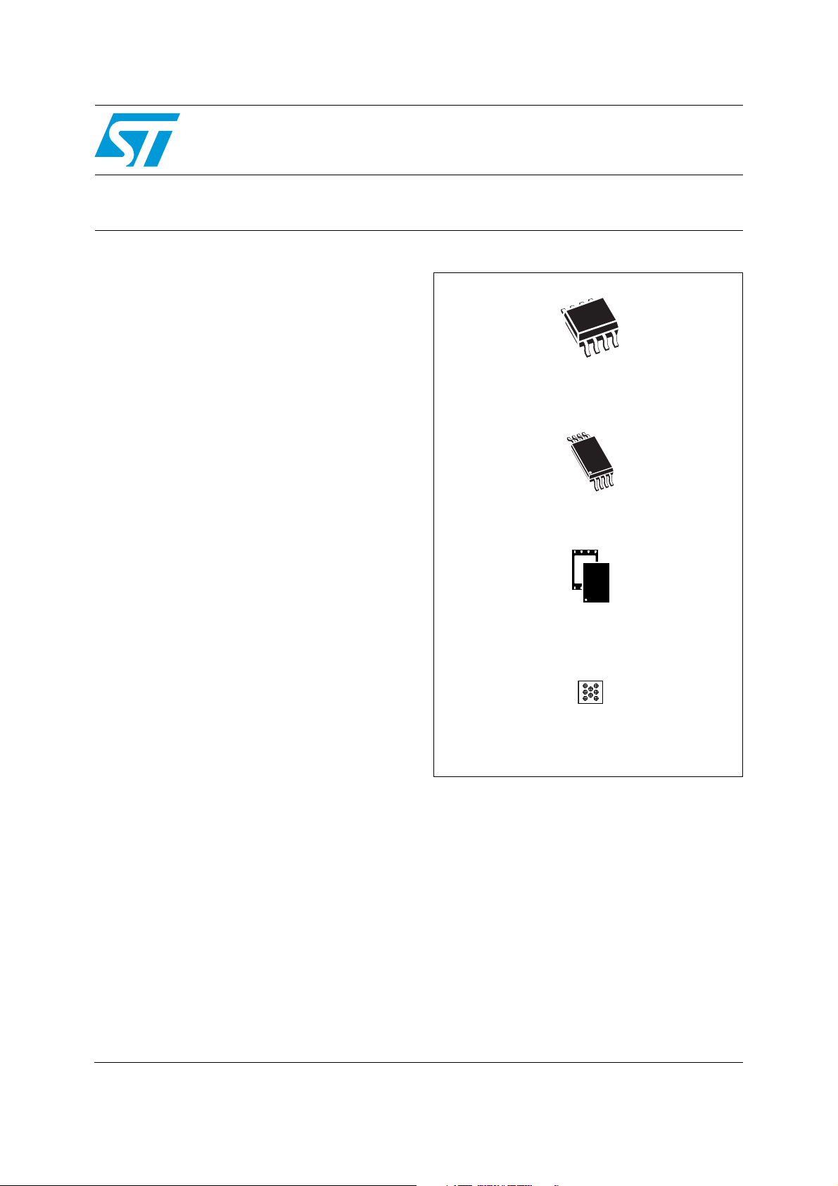
SO8 (MN)
150 mil width
TSSOP8 (DW)
169 mil width
WLCSP (CS)
UFDFPN8 (MC)
2 x 3 mm (MLP)
(preliminary data)
M95512-DR M95512-DF
512-Kbit serial SPI bus EEPROM
Datasheet − production data
Features
■ Compatible with the Serial Peripheral Interface
(SPI) bus
■ Memory array
– 512 Kb (64 Kbytes) of EEPROM
– Page size: 128 bytes
■ Write
– Byte Write within 5 ms
– Page Write within 5 ms
■ Additional Write lockable page (Identification
page)
■ Write Protect: quarter, half or whole memory
array
■ High-speed clock: 10 MHz
■ Single supply voltage:
– 2.5 V to 5.5 V for M95512-W
– 1.8 V to 5.5 V for M95512-R and M95512-
DR
– 1.7 V to 5.5 V for M95512-DF
■ Operating temperature range: from -40°C up to
+85°C
■ Enhanced ESD protection
■ More than 4 million Write cycles
■ More than 200-year data retention
■ Packages
– RoHS compliant and halogen-free
(ECOPACK
®
)
June 2012 Doc ID 11124 Rev 17 1/52
This is information on a product in full production.
www.st.com
1

Contents M95512-W M95512-R M95512-DR M95512-DF
Contents
1 Description . . . . . . . . . . . . . . . . . . . . . . . . . . . . . . . . . . . . . . . . . . . . . . . . . 6
2 Memory organization . . . . . . . . . . . . . . . . . . . . . . . . . . . . . . . . . . . . . . . . 8
3 Signal description . . . . . . . . . . . . . . . . . . . . . . . . . . . . . . . . . . . . . . . . . . . 9
3.1 Serial Data Output (Q) . . . . . . . . . . . . . . . . . . . . . . . . . . . . . . . . . . . . . . . . 9
3.2 Serial Data Input (D) . . . . . . . . . . . . . . . . . . . . . . . . . . . . . . . . . . . . . . . . . 9
3.3 Serial Clock (C) . . . . . . . . . . . . . . . . . . . . . . . . . . . . . . . . . . . . . . . . . . . . . 9
3.4 Chip Select (S
3.5 Hold (HOLD
3.6 Write Protect (W
3.7 V
3.8 V
supply voltage . . . . . . . . . . . . . . . . . . . . . . . . . . . . . . . . . . . . . . . . . . 10
CC
ground . . . . . . . . . . . . . . . . . . . . . . . . . . . . . . . . . . . . . . . . . . . . . . . . 10
SS
) . . . . . . . . . . . . . . . . . . . . . . . . . . . . . . . . . . . . . . . . . . . . . . 9
) . . . . . . . . . . . . . . . . . . . . . . . . . . . . . . . . . . . . . . . . . . . . . . . . 9
) . . . . . . . . . . . . . . . . . . . . . . . . . . . . . . . . . . . . . . . . . . . 10
4 Connecting to the SPI bus . . . . . . . . . . . . . . . . . . . . . . . . . . . . . . . . . . . 11
4.1 SPI modes . . . . . . . . . . . . . . . . . . . . . . . . . . . . . . . . . . . . . . . . . . . . . . . . 12
5 Operating features . . . . . . . . . . . . . . . . . . . . . . . . . . . . . . . . . . . . . . . . . 13
5.1 Supply voltage (VCC) . . . . . . . . . . . . . . . . . . . . . . . . . . . . . . . . . . . . . . . . 13
5.1.1 Operating supply voltage V
5.1.2 Device reset . . . . . . . . . . . . . . . . . . . . . . . . . . . . . . . . . . . . . . . . . . . . . . 13
5.1.3 Power-up conditions . . . . . . . . . . . . . . . . . . . . . . . . . . . . . . . . . . . . . . . 13
5.1.4 Power-down . . . . . . . . . . . . . . . . . . . . . . . . . . . . . . . . . . . . . . . . . . . . . . 14
5.2 Active Power and Standby Power modes . . . . . . . . . . . . . . . . . . . . . . . . . 14
5.3 Hold condition . . . . . . . . . . . . . . . . . . . . . . . . . . . . . . . . . . . . . . . . . . . . . . 14
CC . . . . . . . . . . . . . . . . . . . . . . . . . . . . . . . . . . . . . . . . . 13
5.4 Status Register . . . . . . . . . . . . . . . . . . . . . . . . . . . . . . . . . . . . . . . . . . . . . 15
5.5 Data protection and protocol control . . . . . . . . . . . . . . . . . . . . . . . . . . . . 15
6 Instructions . . . . . . . . . . . . . . . . . . . . . . . . . . . . . . . . . . . . . . . . . . . . . . . 16
6.1 Write Enable (WREN) . . . . . . . . . . . . . . . . . . . . . . . . . . . . . . . . . . . . . . . 17
6.2 Write Disable (WRDI) . . . . . . . . . . . . . . . . . . . . . . . . . . . . . . . . . . . . . . . . 18
6.3 Read Status Register (RDSR) . . . . . . . . . . . . . . . . . . . . . . . . . . . . . . . . . 19
6.3.1 WIP bit . . . . . . . . . . . . . . . . . . . . . . . . . . . . . . . . . . . . . . . . . . . . . . . . . . 19
2/52 Doc ID 11124 Rev 17

M95512-W M95512-R M95512-DR M95512-DF Contents
6.3.2 WEL bit . . . . . . . . . . . . . . . . . . . . . . . . . . . . . . . . . . . . . . . . . . . . . . . . . 19
6.3.3 BP1, BP0 bits . . . . . . . . . . . . . . . . . . . . . . . . . . . . . . . . . . . . . . . . . . . . . 19
6.3.4 SRWD bit . . . . . . . . . . . . . . . . . . . . . . . . . . . . . . . . . . . . . . . . . . . . . . . . 20
6.4 Write Status Register (WRSR) . . . . . . . . . . . . . . . . . . . . . . . . . . . . . . . . . 20
6.5 Read from Memory Array (READ) . . . . . . . . . . . . . . . . . . . . . . . . . . . . . . 22
6.6 Write to Memory Array (WRITE) . . . . . . . . . . . . . . . . . . . . . . . . . . . . . . . 23
6.6.1 Cycling with Error Correction Code (ECC) . . . . . . . . . . . . . . . . . . . . . . 25
6.7 Read Identification Page (available only in M95512-D devices) . . . . . . . . 26
6.8 Write Identification Page (available only in M95512-D devices) . . . . . . . . 27
6.9 Read Lock Status (available only in M95512-D devices) . . . . . . . . . . . . . 28
6.10 Lock ID (available only in M95512-D devices) . . . . . . . . . . . . . . . . . . . . . 29
7 Power-up and delivery state . . . . . . . . . . . . . . . . . . . . . . . . . . . . . . . . . . 30
7.1 Power-up state . . . . . . . . . . . . . . . . . . . . . . . . . . . . . . . . . . . . . . . . . . . . . 30
7.2 Initial delivery state . . . . . . . . . . . . . . . . . . . . . . . . . . . . . . . . . . . . . . . . . . 30
8 Maximum rating . . . . . . . . . . . . . . . . . . . . . . . . . . . . . . . . . . . . . . . . . . . . 31
9 DC and AC parameters . . . . . . . . . . . . . . . . . . . . . . . . . . . . . . . . . . . . . . 32
10 Package mechanical data . . . . . . . . . . . . . . . . . . . . . . . . . . . . . . . . . . . . 42
11 Part numbering . . . . . . . . . . . . . . . . . . . . . . . . . . . . . . . . . . . . . . . . . . . . 47
12 Revision history . . . . . . . . . . . . . . . . . . . . . . . . . . . . . . . . . . . . . . . . . . . 48
Doc ID 11124 Rev 17 3/52

List of tables M95512-W M95512-R M95512-DR M95512-DF
List of tables
Table 1. Signal names . . . . . . . . . . . . . . . . . . . . . . . . . . . . . . . . . . . . . . . . . . . . . . . . . . . . . . . . . . . . 6
Table 2. Write-protected block size . . . . . . . . . . . . . . . . . . . . . . . . . . . . . . . . . . . . . . . . . . . . . . . . . 15
Table 3. Instruction set . . . . . . . . . . . . . . . . . . . . . . . . . . . . . . . . . . . . . . . . . . . . . . . . . . . . . . . . . . . 16
Table 4. M95512-D instruction set . . . . . . . . . . . . . . . . . . . . . . . . . . . . . . . . . . . . . . . . . . . . . . . . . . 16
Table 5. Status Register format . . . . . . . . . . . . . . . . . . . . . . . . . . . . . . . . . . . . . . . . . . . . . . . . . . . . 20
Table 6. Protection modes . . . . . . . . . . . . . . . . . . . . . . . . . . . . . . . . . . . . . . . . . . . . . . . . . . . . . . . . 21
Table 7. Absolute maximum ratings . . . . . . . . . . . . . . . . . . . . . . . . . . . . . . . . . . . . . . . . . . . . . . . . . 31
Table 8. Operating conditions (M95512-W, device grade 6) . . . . . . . . . . . . . . . . . . . . . . . . . . . . . . 32
Table 9. Operating conditions (M95512-R and M95512-DR, device grade 6) . . . . . . . . . . . . . . . . . 32
Table 10. AC measurement conditions. . . . . . . . . . . . . . . . . . . . . . . . . . . . . . . . . . . . . . . . . . . . . . . . 32
Table 11. Capacitance . . . . . . . . . . . . . . . . . . . . . . . . . . . . . . . . . . . . . . . . . . . . . . . . . . . . . . . . . . . . 33
Table 12. Cycling performance by groups of four bytes . . . . . . . . . . . . . . . . . . . . . . . . . . . . . . . . . . . 33
Table 13. Memory cell data retention . . . . . . . . . . . . . . . . . . . . . . . . . . . . . . . . . . . . . . . . . . . . . . . . . 33
Table 14. DC characteristics (previous M95512-W products, device grade 6). . . . . . . . . . . . . . . . . . 34
Table 15. DC characteristics (M95512-W products, device grade 6) . . . . . . . . . . . . . . . . . . . . . . . . . 35
Table 16. DC characteristics (M95512-R and M95512-DR products, device grade 6). . . . . . . . . . . . 35
Table 17. DC characteristics (M95512-DF products, device grade 6) . . . . . . . . . . . . . . . . . . . . . . . . 36
Table 18. AC characteristics (previous M95512-W products, device grade 6) . . . . . . . . . . . . . . . . . . 37
Table 19. AC characteristics (M95512-W products, device grade 6) . . . . . . . . . . . . . . . . . . . . . . . . . 38
Table 20. AC characteristics (M95512-R and M95512-DF products, device grade 6) . . . . . . . . . . . . 39
Table 21. SO8N – 8-lead plastic small outline, 150 mils body width, mechanical data . . . . . . . . . . . 42
Table 22. UFDFPN8 (MLP8) – 8-lead ultra thin fine pitch dual flat package no lead
2 x 3 mm, data . . . . . . . . . . . . . . . . . . . . . . . . . . . . . . . . . . . . . . . . . . . . . . . . . . . . . . . . . . 43
Table 23. TSSOP8 – 8-lead thin shrink small outline, package mechanical data. . . . . . . . . . . . . . . . 44
Table 24. M95512-DFCS6TP/K, WLCSP 8-bump wafer-level chip scale package mechanical data. 46
Table 25. Ordering information scheme . . . . . . . . . . . . . . . . . . . . . . . . . . . . . . . . . . . . . . . . . . . . . . . 47
Table 26. Document revision history . . . . . . . . . . . . . . . . . . . . . . . . . . . . . . . . . . . . . . . . . . . . . . . . . 48
4/52 Doc ID 11124 Rev 17

M95512-W M95512-R M95512-DR M95512-DF List of figures
List of figures
Figure 1. Logic diagram . . . . . . . . . . . . . . . . . . . . . . . . . . . . . . . . . . . . . . . . . . . . . . . . . . . . . . . . . . . . 6
Figure 2. 8-pin package connections (top view) . . . . . . . . . . . . . . . . . . . . . . . . . . . . . . . . . . . . . . . . . 7
Figure 3. WLCSP connections for the die identified by process letters “KB”
(top view, marking side, with balls on the underside) . . . . . . . . . . . . . . . . . . . . . . . . . . . . . 7
Figure 4. Block diagram . . . . . . . . . . . . . . . . . . . . . . . . . . . . . . . . . . . . . . . . . . . . . . . . . . . . . . . . . . . . 8
Figure 5. Bus master and memory devices on the SPI bus . . . . . . . . . . . . . . . . . . . . . . . . . . . . . . . . 11
Figure 6. SPI modes supported . . . . . . . . . . . . . . . . . . . . . . . . . . . . . . . . . . . . . . . . . . . . . . . . . . . . . 12
Figure 7. Hold condition activation . . . . . . . . . . . . . . . . . . . . . . . . . . . . . . . . . . . . . . . . . . . . . . . . . . . 14
Figure 8. Write Enable (WREN) sequence . . . . . . . . . . . . . . . . . . . . . . . . . . . . . . . . . . . . . . . . . . . . 17
Figure 9. Write Disable (WRDI) sequence . . . . . . . . . . . . . . . . . . . . . . . . . . . . . . . . . . . . . . . . . . . . . 18
Figure 10. Read Status Register (RDSR) sequence . . . . . . . . . . . . . . . . . . . . . . . . . . . . . . . . . . . . . . 19
Figure 11. Write Status Register (WRSR) sequence . . . . . . . . . . . . . . . . . . . . . . . . . . . . . . . . . . . . . . 20
Figure 12. Read from Memory Array (READ) sequence . . . . . . . . . . . . . . . . . . . . . . . . . . . . . . . . . . . 22
Figure 13. Byte Write (WRITE) sequence . . . . . . . . . . . . . . . . . . . . . . . . . . . . . . . . . . . . . . . . . . . . . . 23
Figure 14. Page Write (WRITE) sequence . . . . . . . . . . . . . . . . . . . . . . . . . . . . . . . . . . . . . . . . . . . . . 24
Figure 15. Read Identification Page sequence . . . . . . . . . . . . . . . . . . . . . . . . . . . . . . . . . . . . . . . . . . 26
Figure 16. Write identification page sequence. . . . . . . . . . . . . . . . . . . . . . . . . . . . . . . . . . . . . . . . . . . 27
Figure 17. Read Lock Status sequence . . . . . . . . . . . . . . . . . . . . . . . . . . . . . . . . . . . . . . . . . . . . . . . 28
Figure 18. Lock ID sequence . . . . . . . . . . . . . . . . . . . . . . . . . . . . . . . . . . . . . . . . . . . . . . . . . . . . . . . 29
Figure 19. AC measurement I/O waveform . . . . . . . . . . . . . . . . . . . . . . . . . . . . . . . . . . . . . . . . . . . . . 32
Figure 20. Serial input timing . . . . . . . . . . . . . . . . . . . . . . . . . . . . . . . . . . . . . . . . . . . . . . . . . . . . . . . . 40
Figure 21. Hold timing . . . . . . . . . . . . . . . . . . . . . . . . . . . . . . . . . . . . . . . . . . . . . . . . . . . . . . . . . . . . . 40
Figure 22. Serial output timing . . . . . . . . . . . . . . . . . . . . . . . . . . . . . . . . . . . . . . . . . . . . . . . . . . . . . . . 41
Figure 23. SO8N – 8-lead plastic small outline, 150 mils body width, package outline . . . . . . . . . . . . 42
Figure 24. UFDFPN8 (MLP8) – 8-lead ultra thin fine pitch dual flat no lead, package outline. . . . . . . 43
Figure 25. TSSOP8 – 8-lead thin shrink small outline, package outline . . . . . . . . . . . . . . . . . . . . . . . 44
Figure 26. M95512-DFCS6TP/K, WLCSP 8-bump wafer-level chip scale package outline . . . . . . . . 45
Doc ID 11124 Rev 17 5/52
Description M95512-W M95512-R M95512-DR M95512-DF
AI01789C
S
V
CC
M95xxx
HOLD
V
SS
W
Q
C
D
1 Description
The M95512 devices are Electrically Erasable PROgrammable Memories (EEPROMs)
organized as 65536 x 8 bits, accessed through the SPI bus.
The M95512-W can operate with a supply voltage from 2.5 V to 5.5 V, the M95512-R and
M95512-DR can operate with a supply voltage from 1.8 V to 5.5 V, and the M95512-DF can
operate with a supply voltage from 1.7 V to 5.5 V, over an ambient temperature range of
-40 °C / +85 °C.
The M95512-D offers an additional page, named the Identification Page (128 bytes). The
Identification Page can be used to store sensitive application parameters which can be
(later) permanently locked in Read-only mode.
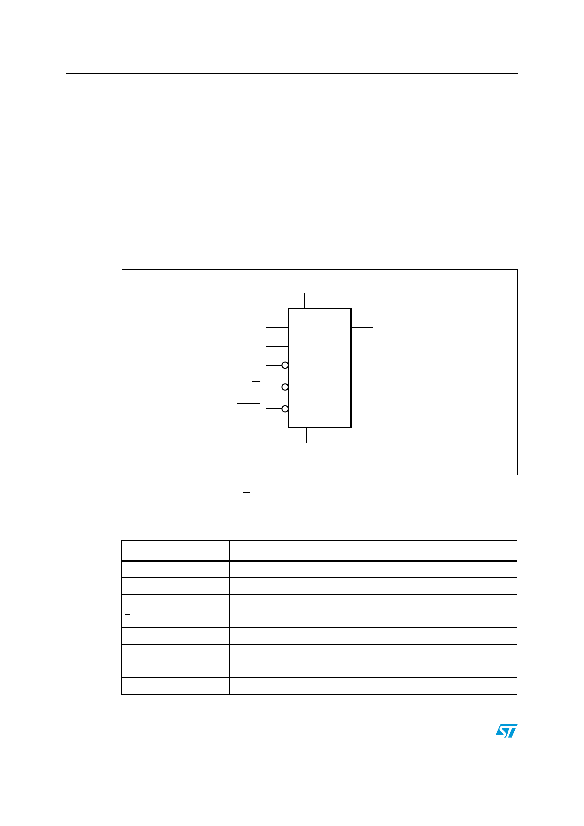
Figure 1. Logic diagram
The SPI bus signals are C, D and Q, as shown in Figure 1 and Tab l e 1 . The device is
selected when Chip Select (S
interrupted when the HOLD
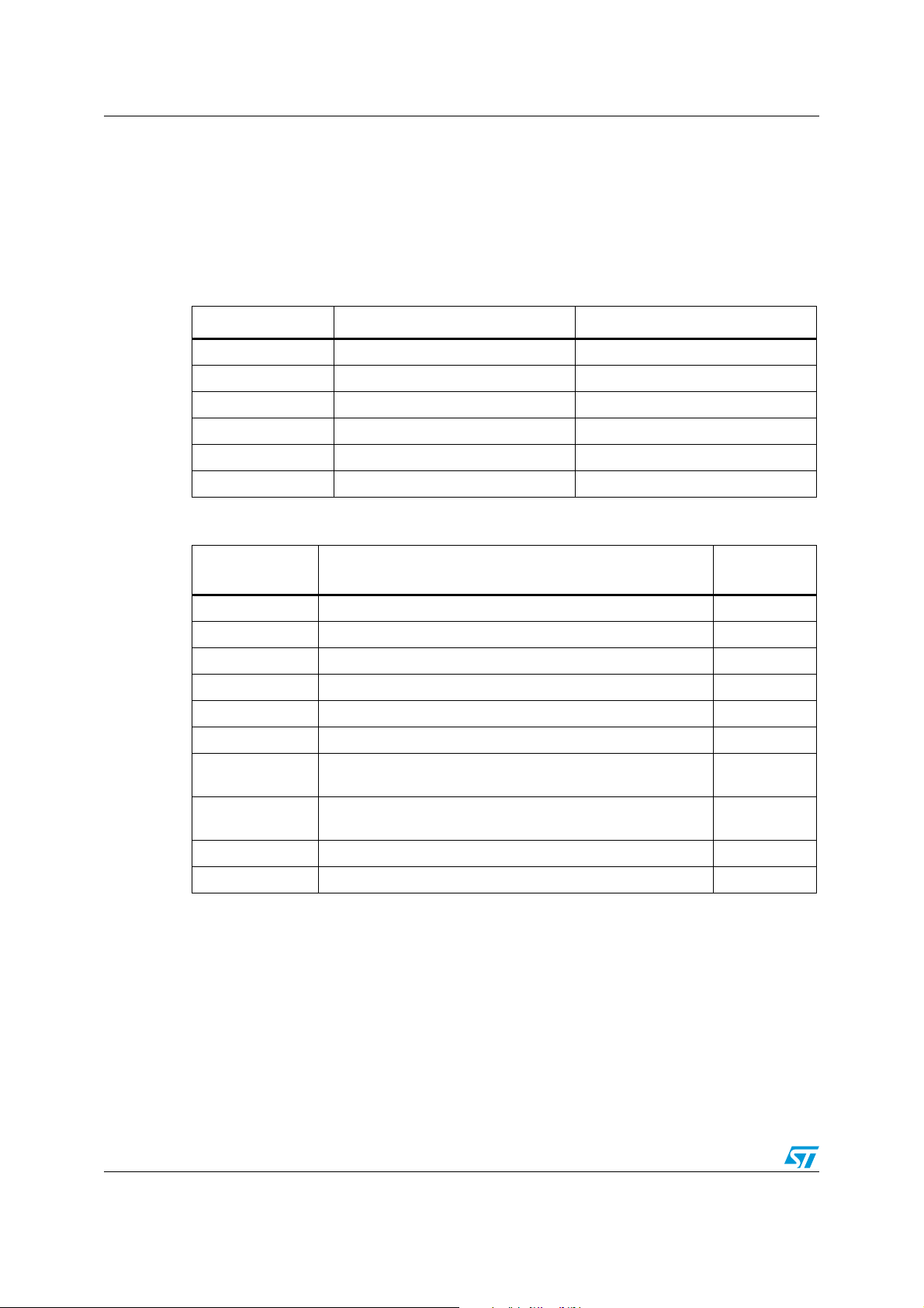
Table 1. Signal names
Signal name Function Direction
C Serial Clock Input
D Serial Data Input Input
Q Serial Data Output Output
S
6/52 Doc ID 11124 Rev 17
W
Hold Input
HOLD
V
CC
V
SS
) is driven low. Communications with the device can be
is driven low.
Chip Select Input
Write Protect Input
Supply voltage
Ground
M95512-W M95512-R M95512-DR M95512-DF Description
DV
SS
C
HOLDQ
SV
CC
W
AI01790D
M95xxx
1
2
3
4
8
7
6
5
-36
6
##
$
6
33
3
#
(/,$
7
1
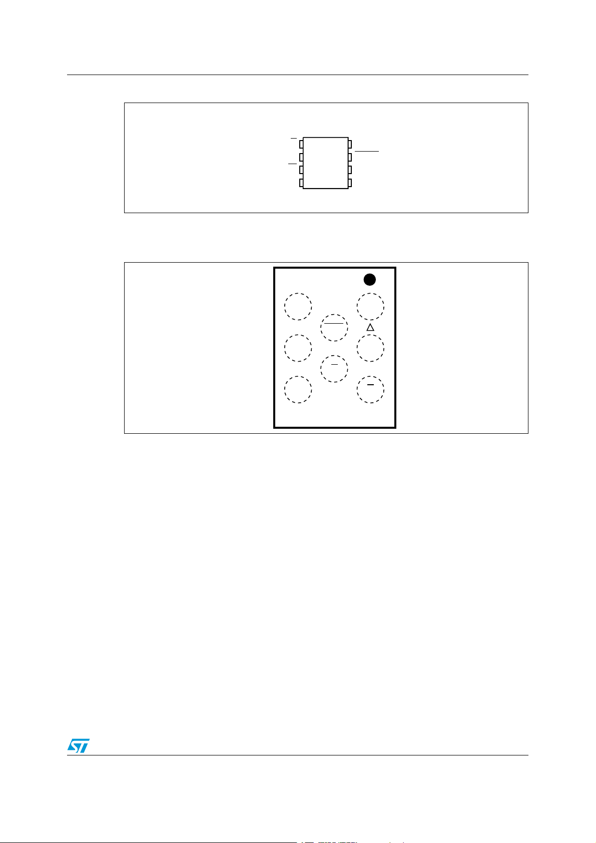
Figure 2. 8-pin package connections (top view)
1. See Section 10: Package mechanical data section for package dimensions, and how to identify pin 1.
Figure 3. WLCSP connections for the die identified by process letters “KB”
(top view, marking side, with balls on the underside)
Caution: As EEPROM cells lose their charge (and so their binary value) when exposed to ultra violet
(UV) light, EEPROM dice delivered in wafer form or in WLCSP package by
STMicroelectronics must never be exposed to UV light.
Doc ID 11124 Rev 17 7/52
Memory organization M95512-W M95512-R M95512-DR M95512-DF
-36
(/,$
3
7
#ONTROLLOGIC
(IGHVOLTAGE
GENERATOR
)/SHIFTREGISTER
!DDRESSREGISTER
ANDCOUNTER
$ATA
REGISTER
PAGE
8DECODER
9DECODER
#
$
1
3IZEOFTHE
2EADONLY
%%02/AREA
3TATUS
REGISTER
)DENTIFICATIONPAGE
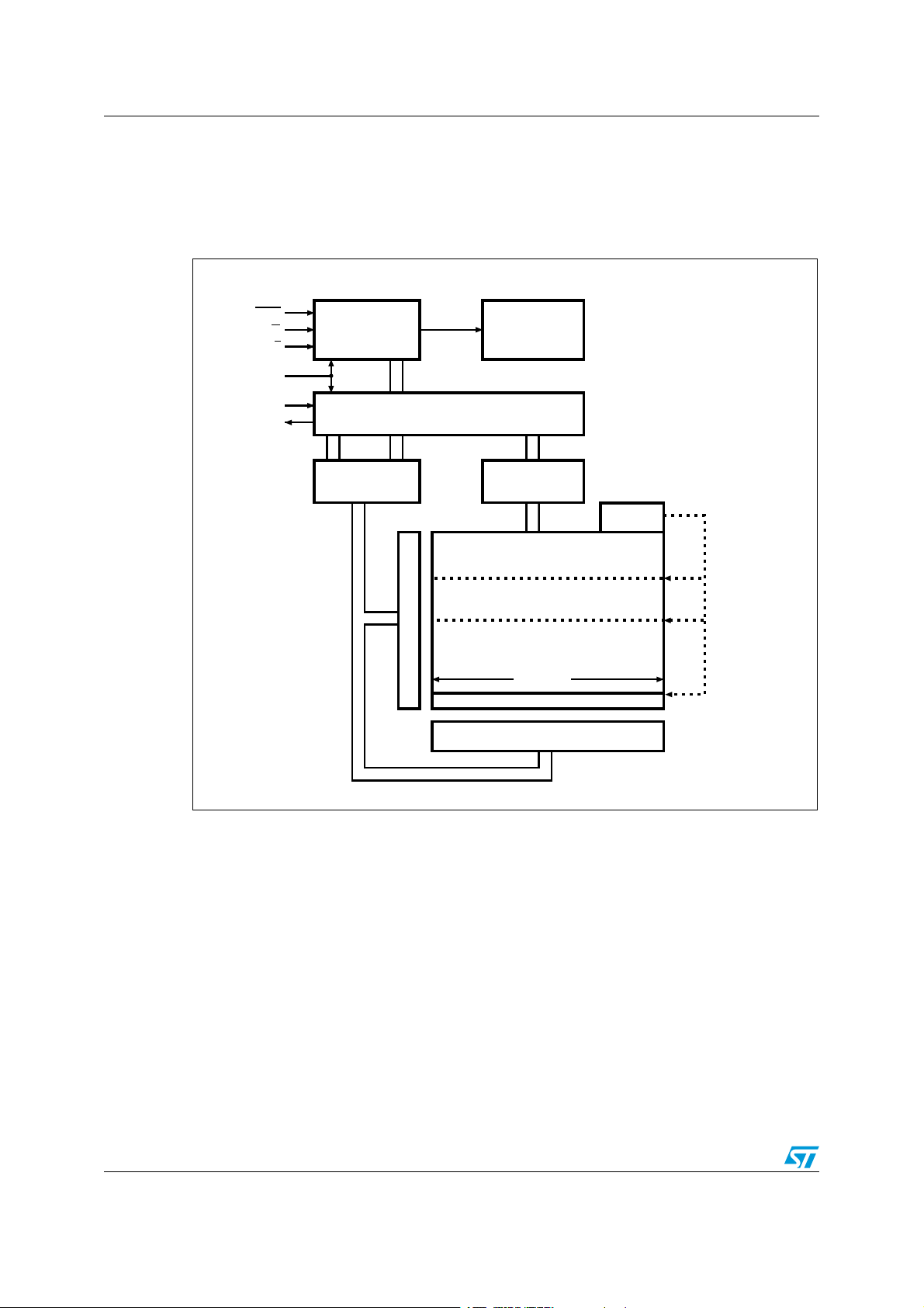
2 Memory organization
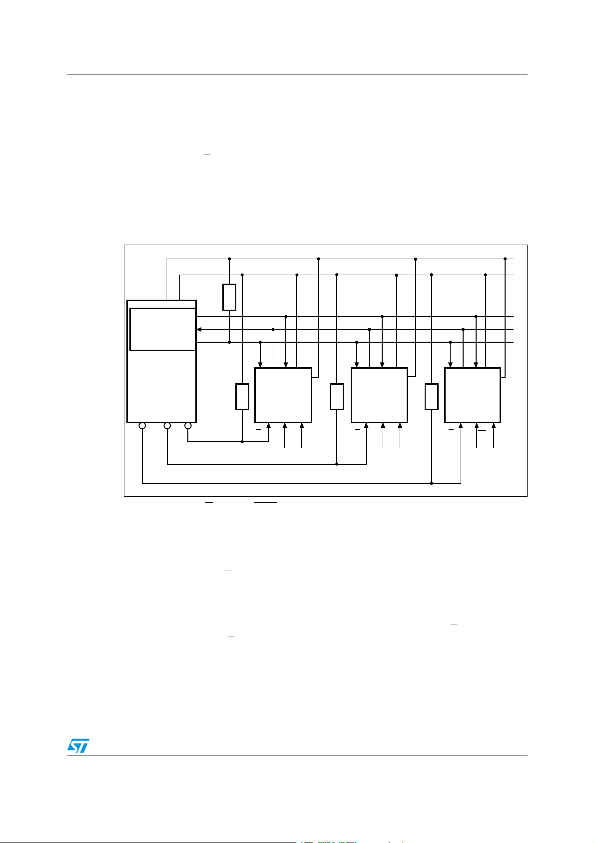
The memory is organized as shown in the following figure.
Figure 4. Block diagram
8/52 Doc ID 11124 Rev 17

M95512-W M95512-R M95512-DR M95512-DF Signal description
3 Signal description
During all operations, VCC must be held stable and within the specified valid range:
V
(min) to VCC(max).
CC
All of the input and output signals must be held high or low (according to voltages of V
V
, VIL or VOL, as specified in Section 9: DC and AC parameters). These signals are
OH
described next.
3.1 Serial Data Output (Q)
This output signal is used to transfer data serially out of the device. Data is shifted out on the
falling edge of Serial Clock (C).
3.2 Serial Data Input (D)
This input signal is used to transfer data serially into the device. It receives instructions,
addresses, and the data to be written. Values are latched on the rising edge of Serial Clock
(C).
,
IH
3.3 Serial Clock (C)
This input signal provides the timing of the serial interface. Instructions, addresses, or data
present at Serial Data Input (D) are latched on the rising edge of Serial Clock (C). Data on
Serial Data Output (Q) change from the falling edge of Serial Clock (C).
3.4 Chip Select (S)
When this input signal is high, the device is deselected and Serial Data Output (Q) is at high
impedance. The device is in the Standby Power mode, unless an internal Write cycle is in
progress. Driving Chip Select (S
After power-up, a falling edge on Chip Select (S
instruction.
3.5 Hold (HOLD)
The Hold (HOLD) signal is used to pause any serial communications with the device without
deselecting the device.
During the Hold condition, the Serial Data Output (Q) is high impedance, and Serial Data
Input (D) and Serial Clock (C) are Don’t Care.
To start the Hold condition, the device must be selected, with Chip Select (S
) low selects the device, placing it in the Active Power mode.
) is required prior to the start of any
) driven low.
Doc ID 11124 Rev 17 9/52

Signal description M95512-W M95512-R M95512-DR M95512-DF
3.6 Write Protect (W)
The main purpose of this input signal is to freeze the size of the area of memory that is
protected against Write instructions (as specified by the values in the BP1 and BP0 bits of
the Status Register).
This pin must be driven either high or low, and must be stable during all Write instructions.
3.7 V
supply voltage
CC
VCC is the supply voltage.
3.8 VSS ground
VSS is the reference for all signals, including the VCC supply voltage.
10/52 Doc ID 11124 Rev 17
M95512-W M95512-R M95512-DR M95512-DF Connecting to the SPI bus
AI12836b
SPI Bus Master
SPI Memory
Device
SDO
SDI
SCK
CQD
S
SPI Memory
Device
CQD
S
SPI Memory
Device
CQD
S
CS3 CS2 CS1
SPI Interface with
(CPOL, CPHA) =
(0, 0) or (1, 1)
W
HOLD
W
HOLD
W
HOLD
RR R
V
CC
V
CC
V
CC
V
CC
V
SS
V
SS
V
SS
V
SS
R
4 Connecting to the SPI bus
All instructions, addresses and input data bytes are shifted in to the device, most significant
bit first. The Serial Data Input (D) is sampled on the first rising edge of the Serial Clock (C)
after Chip Select (S
All output data bytes are shifted out of the device, most significant bit first. The Serial Data
Output (Q) is latched on the first falling edge of the Serial Clock (C) after the instruction
(such as the Read from Memory Array and Read Status Register instructions) have been
clocked into the device.
Figure 5. Bus master and memory devices on the SPI bus
) goes low.
1. The Write Protect (W) and Hold (HOLD) signals should be driven, high or low as appropriate.
Figure 5 shows an example of three memory devices connected to an SPI bus master. Only
one memory device is selected at a time, so only one memory device drives the Serial Data
Output (Q) line at a time. The other memory devices are high impedance.
The pull-up resistor R (represented in Figure 5) ensures that a device is not selected if the
Bus Master leaves the S
line in the high impedance state.
In applications where the Bus Master may leave all SPI bus lines in high impedance at the
same time (for example, if the Bus Master is reset during the transmission of an instruction),
the clock line (C) must be connected to an external pull-down resistor so that, if all
inputs/outputs become high impedance, the C line is pulled low (while the S
high): this ensures that S
t
requirement is met. The typical value of R is 100 kΩ..
SHCH
and C do not become high at the same time, and so, that the
Doc ID 11124 Rev 17 11/52
line is pulled
Connecting to the SPI bus M95512-W M95512-R M95512-DR M95512-DF
AI01438B
C
MSB
CPHA
D
0
1
CPOL
0
1
Q
C
MSB
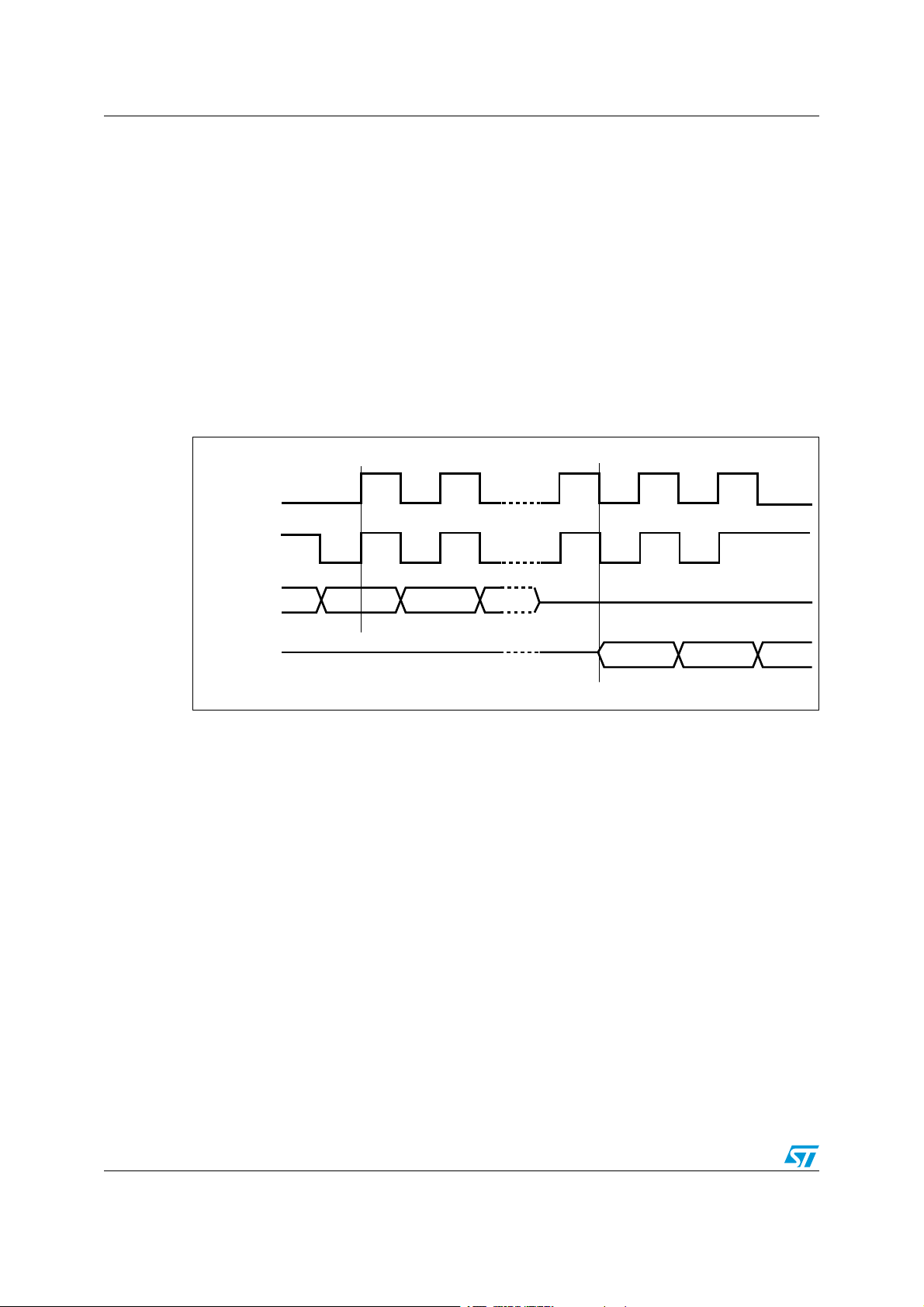
4.1 SPI modes
These devices can be driven by a microcontroller with its SPI peripheral running in either of
the following two modes:
● CPOL=0, CPHA=0
● CPOL=1, CPHA=1
For these two modes, input data is latched in on the rising edge of Serial Clock (C), and
output data is available from the falling edge of Serial Clock (C).
The difference between the two modes, as shown in Figure 6, is the clock polarity when the
bus master is in Stand-by mode and not transferring data:
● C remains at 0 for (CPOL=0, CPHA=0)
● C remains at 1 for (CPOL=1, CPHA=1)
Figure 6. SPI modes supported
12/52 Doc ID 11124 Rev 17

M95512-W M95512-R M95512-DR M95512-DF Operating features
5 Operating features
5.1 Supply voltage (VCC)
5.1.1 Operating supply voltage V
Prior to selecting the memory and issuing instructions to it, a valid and stable VCC voltage
within the specified [V
(min), VCC(max)] range must be applied (see Operating conditions
CC
in Section 9: DC and AC parameters). This voltage must remain stable and valid until the
end of the transmission of the instruction and, for a Write instruction, until the completion of
the internal write cycle (t
recommended to decouple the V
10 nF to 100 nF) close to the V
). In order to secure a stable DC supply voltage, it is
W
CC
CC/VSS
5.1.2 Device reset
In order to prevent erroneous instruction decoding and inadvertent Write operations during
power-up, a power-on-reset (POR) circuit is included. At power-up, the device does not
respond to any instruction until VCC reaches the POR threshold voltage. This threshold is
lower than the minimum V
and AC parameters).
At power-up, when V
CC
following state:
● in Standby Power mode,
● deselected,
● Status Register values:
– The Write Enable Latch (WEL) bit is reset to 0.
– The Write In Progress (WIP) bit is reset to 0.
– The SRWD, BP1 and BP0 bits remain unchanged (non-volatile bits).
operating voltage (see Operating conditions in Section 9: DC
CC
passes over the POR threshold, the device is reset and is in the
CC
line with a suitable capacitor (usually of the order of
device pins.
It is important to note that the device must not be accessed until V
stable level within the specified [V
conditions in Section 9: DC and AC parameters.
5.1.3 Power-up conditions
When the power supply is turned on, VCC rises continuously from VSS to VCC. During this
time, the Chip Select (S
therefore recommended to connect the S
Figure 5).
In addition, the Chip Select (S
sensitive as well as level-sensitive: after power-up, the device does not become selected
until a falling edge has first been detected on Chip Select (S
(S
) must have been high, prior to going low to start the first operation.
The V
voltage has to rise continuously from 0 V up to the minimum VCC operating voltage
CC
defined under Operating conditions in Section 9: DC and AC parameters, and the rise time
must not vary faster than 1 V/µs.
) line is not allowed to float but should follow the VCC voltage. It is
reaches a valid and
(min), VCC(max)] range, as defined under Operating
CC
CC
line to VCC via a suitable pull-up resistor (see
) input offers a built-in safety feature, as the S input is edge-
). This ensures that Chip Select
Doc ID 11124 Rev 17 13/52
Operating features M95512-W M95512-R M95512-DR M95512-DF
ai02029E
c
HOLD
Hold
condition
Hold
condition
5.1.4 Power-down
During power-down (continuous decrease of the VCC supply voltage below the minimum
V
operating voltage defined under Operating conditions in Section 9: DC and AC
CC
parameters), the device must be:
● deselected (Chip Select S should be allowed to follow the voltage applied on V
● in Standby Power mode (there should not be any internal write cycle in progress).
CC
),
5.2 Active Power and Standby Power modes
When Chip Select (S) is low, the device is selected, and in the Active Power mode. The
device consumes I
When Chip Select (S
.
CC
) is high, the device is deselected. If a Write cycle is not currently in
progress, the device then goes into the Standby Power mode, and the device consumption
drops to I
, as specified in DC characteristics (see Section 9: DC and AC parameters).
CC1
5.3 Hold condition
The Hold (HOLD) signal is used to pause any serial communications with the device without
resetting the clocking sequence.
To enter the Hold condition, the device must be selected, with Chip Select (S
) low.
During the Hold condition, the Serial Data Output (Q) is high impedance, and the Serial
Data Input (D) and the Serial Clock (C) are Don’t Care.
Normally, the device is kept selected for the whole duration of the Hold condition.
Deselecting the device while it is in the Hold condition has the effect of resetting the state of
the device, and this mechanism can be used if required to reset any processes that had
been in progress.
(a)(b)
Figure 7. Hold condition activation
The Hold condition starts when the Hold (HOLD) signal is driven low when Serial Clock (C)
is already low (as shown in Figure 7).
a. This resets the internal logic, except the WEL and WIP bits of the Status Register.
b. In the specific case where the device has shifted in a Write command (Inst + Address + data bytes, each data
byte being exactly 8 bits), deselecting the device also triggers the Write cycle of this decoded command.
14/52 Doc ID 11124 Rev 17
M95512-W M95512-R M95512-DR M95512-DF Operating features
The Hold condition ends when the Hold (HOLD) signal is driven high when Serial Clock (C)
is already low.
Figure 7 also shows what happens if the rising and falling edges are not timed to coincide
with Serial Clock (C) being low.
5.4 Status Register
The Status Register contains a number of status and control bits that can be read or set (as
appropriate) by specific instructions. See Section 6.3: Read Status Register (RDSR) for a
detailed description of the Status Register bits.
5.5 Data protection and protocol control
The device features the following data protection mechanisms:
● Before accepting the execution of the Write and Write Status Register instructions, the
device checks whether the number of clock pulses comprised in the instructions is a
multiple of eight.
● All instructions that modify data must be preceded by a Write Enable (WREN)
instruction to set the Write Enable Latch (WEL) bit.
● The Block Protect (BP1, BP0) bits in the Status Register are used to configure part of
the memory as read-only.
● The Write Protect (W) signal is used to protect the Block Protect (BP1, BP0) bits in the
Status Register.
For any instruction to be accepted, and executed, Chip Select (S
) must be driven high after
the rising edge of Serial Clock (C) for the last bit of the instruction, and before the next rising
edge of Serial Clock (C).
Two points should be noted in the previous sentence:
● The “last bit of the instruction” can be the eighth bit of the instruction code, or the eighth
bit of a data byte, depending on the instruction (except for Read Status Register
(RDSR) and Read (READ) instructions).
● The “next rising edge of Serial Clock (C)” might (or might not) be the next bus
transaction for some other device on the SPI bus.
Table 2. Write-protected block size
Status Register bits
Protected block Protected array addresses
BP1 BP0
0 0 none none
0 1 Upper quarter C000h - FFFFh
1 0 Upper half 8000h - FFFFh
1 1 Whole memory 0000h - FFFFh
Doc ID 11124 Rev 17 15/52
Instructions M95512-W M95512-R M95512-DR M95512-DF
6 Instructions
Each instruction starts with a single-byte code, as summarized in Ta b le 3 .
If an invalid instruction is sent (one not contained in Ta bl e 3 ), the device automatically
deselects itself.
Table 3. Instruction set
Instruction Description Instruction format
WREN Write Enable 0000 0110
WRDI Write Disable 0000 0100
RDSR Read Status Register 0000 0101
WRSR Write Status Register 0000 0001
READ Read from Memory Array 0000 0011
WRITE Write to Memory Array 0000 0010
Table 4. M95512-D instruction set
Instruction Description
Instruction
format
WREN Write Enable 0000 0110
WRDI Write Disable 0000 0100
RDSR Read Status Register 0000 0101
WRSR Write Status Register 0000 0001
READ Read from Memory Array 0000 0011
WRITE Write to Memory Array 0000 0010
Read Identification
Page
Write Identification
Page
Reads the page dedicated to identification. 1000 0011
Writes the page dedicated to identification. 1000 0010
Read Lock Status Reads the lock status of the Identification Page. 1000 0011
Lock ID Locks the Identification page in read-only mode. 1000 0010
1. Address bit A10 must be 0, all other address bits are Don't Care.
2. Address bit A10 must be 1, all other address bits are Don't Care.
(1)
(1)
(2)
(2)
16/52 Doc ID 11124 Rev 17
 Loading...