


查询M95320-MB3供应商
M95320 M95320-W M95320-R M95320-S
M95640 M95640-W M95640-R M95640-S
32Kbit and 64Kbit Serial SPI Bus EEPROMs
FEATURES SUMMARY
■ Compatible with SPI Bus Serial Interface
(Positive Clock SPI Modes)
■ Single Supply Voltage:
– 4.5 to 5.5V for M95320 and M95640
– 2.5 to 5.5V for M95320-W and M95320-W
– 1.8 to 5.5V for M95320-R and M95640-R
– 1.65 to 5.5V for M95320-S and M95640-S
■ 20MHz, 10MHz, 5MHz or 2MHz clock rates
■ 5ms or 10ms Write Time
■ Status Register
■ Hardware Protection of the Status Register
■ BYTE and PAGE WRITE (up to 32 Bytes)
■ Self-Timed Programming Cycle
■ Adjustable Size Read-Only EEPROM Area
■ Enhanced ESD Protection
■ More than 100000 or 1 million Erase/Write
Cycles (depending on ordering options)
■ More than 40-Year Data Retention
Table 1. Product List
Reference Part Number
M95320
M95320-W
M95320
M95320-R
M95320-S
M95640
M95640-W
M95640
M95640-R
M95640-S
With High Speed Clock
Figure 1. Packages
8
1
PDIP8 (BN)
0.25 mm frame
8
1
SO8 (MN)
150 mil width
TSSOP8 (DW)
169 mil width
MLP8 (MB)
2x3 mm
1/42May 2005

M95640, M95320
TABLE OF CONTENTS
FEATURES SUMMARY . . . . . . . . . . . . . . . . . . . . . . . . . . . . . . . . . . . . . . . . . . . . . . . . . . . . . . . . . . . . . 1
Table 1. Product List . . . . . . . . . . . . . . . . . . . . . . . . . . . . . . . . . . . . . . . . . . . . . . . . . . . . . . . . . . . . 1
Figure 1. Packages. . . . . . . . . . . . . . . . . . . . . . . . . . . . . . . . . . . . . . . . . . . . . . . . . . . . . . . . . . . . . . 1
SUMMARY DESCRIPTION. . . . . . . . . . . . . . . . . . . . . . . . . . . . . . . . . . . . . . . . . . . . . . . . . . . . . . . . . . . 5
Table 2. How to Identify Previous, Current and New Products by the Process Identification Letter 5
Figure 2. Logic Diagram . . . . . . . . . . . . . . . . . . . . . . . . . . . . . . . . . . . . . . . . . . . . . . . . . . . . . . . . . . 5
Figure 3. 8 Pin Package Connections. . . . . . . . . . . . . . . . . . . . . . . . . . . . . . . . . . . . . . . . . . . . . . . .5
Table 3. Signal Names . . . . . . . . . . . . . . . . . . . . . . . . . . . . . . . . . . . . . . . . . . . . . . . . . . . . . . . . . . 5
SIGNAL DESCRIPTION . . . . . . . . . . . . . . . . . . . . . . . . . . . . . . . . . . . . . . . . . . . . . . . . . . . . . . . . . . . . . 6
Serial Data Output (Q). . . . . . . . . . . . . . . . . . . . . . . . . . . . . . . . . . . . . . . . . . . . . . . . . . . . . . . . . . . . 6
Serial Data Input (D) . . . . . . . . . . . . . . . . . . . . . . . . . . . . . . . . . . . . . . . . . . . . . . . . . . . . . . . . . . . . . 6
Serial Clock (C) . . . . . . . . . . . . . . . . . . . . . . . . . . . . . . . . . . . . . . . . . . . . . . . . . . . . . . . . . . . . . . . . . 6
Chip Select (S) . . . . . . . . . . . . . . . . . . . . . . . . . . . . . . . . . . . . . . . . . . . . . . . . . . . . . . . . . . . . . . . . . 6
Hold (HOLD) . . . . . . . . . . . . . . . . . . . . . . . . . . . . . . . . . . . . . . . . . . . . . . . . . . . . . . . . . . . . . . . . . . . 6
Write Protect (W) . . . . . . . . . . . . . . . . . . . . . . . . . . . . . . . . . . . . . . . . . . . . . . . . . . . . . . . . . . . . . . . . 6
CONNECTING TO THE SPI BUS . . . . . . . . . . . . . . . . . . . . . . . . . . . . . . . . . . . . . . . . . . . . . . . . . . . . . . 7
Figure 4. Bus Master and Memory Devices on the SPI Bus. . . . . . . . . . . . . . . . . . . . . . . . . . . . . . . 7
SPI Modes . . . . . . . . . . . . . . . . . . . . . . . . . . . . . . . . . . . . . . . . . . . . . . . . . . . . . . . . . . . . . . . . . . . . 8
Figure 5. SPI Modes Supported . . . . . . . . . . . . . . . . . . . . . . . . . . . . . . . . . . . . . . . . . . . . . . . . . . . . 8
OPERATING FEATURES . . . . . . . . . . . . . . . . . . . . . . . . . . . . . . . . . . . . . . . . . . . . . . . . . . . . . . . . . . . . 9
Power-Up . . . . . . . . . . . . . . . . . . . . . . . . . . . . . . . . . . . . . . . . . . . . . . . . . . . . . . . . . . . . . . . . . . . . . 9
. . . . . . . . . . . . . . . . . . . . . . . . . . . . . . . . . . . . . . . . . . . . . . . . . . . . . . . . . . . . . . . . . . . . . . . . . . . . . . 9
Power On Reset: VCC Lock-Out Write Protect . . . . . . . . . . . . . . . . . . . . . . . . . . . . . . . . . . . . . . . 9
Power-down . . . . . . . . . . . . . . . . . . . . . . . . . . . . . . . . . . . . . . . . . . . . . . . . . . . . . . . . . . . . . . . . . . . 9
Active Power and Standby Power Modes . . . . . . . . . . . . . . . . . . . . . . . . . . . . . . . . . . . . . . . . . . . 9
Hold Condition. . . . . . . . . . . . . . . . . . . . . . . . . . . . . . . . . . . . . . . . . . . . . . . . . . . . . . . . . . . . . . . . . 9
Figure 6. Hold Condition Activation. . . . . . . . . . . . . . . . . . . . . . . . . . . . . . . . . . . . . . . . . . . . . . . . . 10
. . . . . . . . . . . . . . . . . . . . . . . . . . . . . . . . . . . . . . . . . . . . . . . . . . . . . . . . . . . . . . . . . . . . . . . . . . . . . 10
Status Register . . . . . . . . . . . . . . . . . . . . . . . . . . . . . . . . . . . . . . . . . . . . . . . . . . . . . . . . . . . . . . . 10
WIP bit. . . . . . . . . . . . . . . . . . . . . . . . . . . . . . . . . . . . . . . . . . . . . . . . . . . . . . . . . . . . . . . . . . . . . . . 10
WEL bit . . . . . . . . . . . . . . . . . . . . . . . . . . . . . . . . . . . . . . . . . . . . . . . . . . . . . . . . . . . . . . . . . . . . . . 10
BP1, BP0 bits . . . . . . . . . . . . . . . . . . . . . . . . . . . . . . . . . . . . . . . . . . . . . . . . . . . . . . . . . . . . . . . . . 10
SRWD bit. . . . . . . . . . . . . . . . . . . . . . . . . . . . . . . . . . . . . . . . . . . . . . . . . . . . . . . . . . . . . . . . . . . . . 10
Table 4. Status Register Format . . . . . . . . . . . . . . . . . . . . . . . . . . . . . . . . . . . . . . . . . . . . . . . . . . 10
. . . . . . . . . . . . . . . . . . . . . . . . . . . . . . . . . . . . . . . . . . . . . . . . . . . . . . . . . . . . . . . . . . . . . . . . . . . . . 10
Data Protection and Protocol Control . . . . . . . . . . . . . . . . . . . . . . . . . . . . . . . . . . . . . . . . . . . . . 10
Table 5. Write-Protected Block Size . . . . . . . . . . . . . . . . . . . . . . . . . . . . . . . . . . . . . . . . . . . . . . .11
MEMORY ORGANIZATION . . . . . . . . . . . . . . . . . . . . . . . . . . . . . . . . . . . . . . . . . . . . . . . . . . . . . . . . . 12
2/42

M95640, M95320
Figure 7. Block Diagram . . . . . . . . . . . . . . . . . . . . . . . . . . . . . . . . . . . . . . . . . . . . . . . . . . . . . . . . . 12
INSTRUCTIONS . . . . . . . . . . . . . . . . . . . . . . . . . . . . . . . . . . . . . . . . . . . . . . . . . . . . . . . . . . . . . . . . . . 13
Table 6. Instruction Set . . . . . . . . . . . . . . . . . . . . . . . . . . . . . . . . . . . . . . . . . . . . . . . . . . . . . . . . . 13
Write Enable (WREN) . . . . . . . . . . . . . . . . . . . . . . . . . . . . . . . . . . . . . . . . . . . . . . . . . . . . . . . . . . 14
Figure 8. Write Enable (WREN) Sequence. . . . . . . . . . . . . . . . . . . . . . . . . . . . . . . . . . . . . . . . . . . 14
Write Disable (WRDI). . . . . . . . . . . . . . . . . . . . . . . . . . . . . . . . . . . . . . . . . . . . . . . . . . . . . . . . . . . 14
Figure 9. Write Disable (WRDI) Sequence. . . . . . . . . . . . . . . . . . . . . . . . . . . . . . . . . . . . . . . . . . . 14
Read Status Register (RDSR). . . . . . . . . . . . . . . . . . . . . . . . . . . . . . . . . . . . . . . . . . . . . . . . . . . . 15
WIP bit. . . . . . . . . . . . . . . . . . . . . . . . . . . . . . . . . . . . . . . . . . . . . . . . . . . . . . . . . . . . . . . . . . . . . . . 15
WEL bit . . . . . . . . . . . . . . . . . . . . . . . . . . . . . . . . . . . . . . . . . . . . . . . . . . . . . . . . . . . . . . . . . . . . . . 15
BP1, BP0 bits . . . . . . . . . . . . . . . . . . . . . . . . . . . . . . . . . . . . . . . . . . . . . . . . . . . . . . . . . . . . . . . . . 15
SRWD bit. . . . . . . . . . . . . . . . . . . . . . . . . . . . . . . . . . . . . . . . . . . . . . . . . . . . . . . . . . . . . . . . . . . . . 15
Figure 10.Read Status Register (RDSR) Sequence . . . . . . . . . . . . . . . . . . . . . . . . . . . . . . . . . . . . 15
Write Status Register (WRSR) . . . . . . . . . . . . . . . . . . . . . . . . . . . . . . . . . . . . . . . . . . . . . . . . . . . 16
Table 7. Protection Modes. . . . . . . . . . . . . . . . . . . . . . . . . . . . . . . . . . . . . . . . . . . . . . . . . . . . . . . 16
Table 8. Address Range Bits. . . . . . . . . . . . . . . . . . . . . . . . . . . . . . . . . . . . . . . . . . . . . . . . . . . . . 17
Figure 11.Write Status Register (WRSR) Sequence. . . . . . . . . . . . . . . . . . . . . . . . . . . . . . . . . . . . 17
Read from Memory Array (READ) . . . . . . . . . . . . . . . . . . . . . . . . . . . . . . . . . . . . . . . . . . . . . . . . 18
Figure 12.Read from Memory Array (READ) Sequence . . . . . . . . . . . . . . . . . . . . . . . . . . . . . . . . . 18
Write to Memory Array (WRITE). . . . . . . . . . . . . . . . . . . . . . . . . . . . . . . . . . . . . . . . . . . . . . . . . .19
Figure 13.Byte Write (WRITE) Sequence . . . . . . . . . . . . . . . . . . . . . . . . . . . . . . . . . . . . . . . . . . . . 19
Figure 14.Page Write (WRITE) Sequence . . . . . . . . . . . . . . . . . . . . . . . . . . . . . . . . . . . . . . . . . . . 20
POWER-UP AND DELIVERY STATE. . . . . . . . . . . . . . . . . . . . . . . . . . . . . . . . . . . . . . . . . . . . . . . . . . 21
Power-up State . . . . . . . . . . . . . . . . . . . . . . . . . . . . . . . . . . . . . . . . . . . . . . . . . . . . . . . . . . . . . . . 21
INITIAL DELIVERY STATE. . . . . . . . . . . . . . . . . . . . . . . . . . . . . . . . . . . . . . . . . . . . . . . . . . . . . . . . . . 21
MAXIMUM RATING. . . . . . . . . . . . . . . . . . . . . . . . . . . . . . . . . . . . . . . . . . . . . . . . . . . . . . . . . . . . . . . . 22
Table 9. Absolute Maximum Ratings. . . . . . . . . . . . . . . . . . . . . . . . . . . . . . . . . . . . . . . . . . . . . . . 22
DC AND AC PARAMETERS. . . . . . . . . . . . . . . . . . . . . . . . . . . . . . . . . . . . . . . . . . . . . . . . . . . . . . . . . 23
Table 10. Operating Conditions (M95320 and M95640) . . . . . . . . . . . . . . . . . . . . . . . . . . . . . . . . . 23
Table 11. Operating Conditions (M95320-W and M95640-W) . . . . . . . . . . . . . . . . . . . . . . . . . . . . 23
Table 12. Operating Conditions (M95320-R and M95640-R) . . . . . . . . . . . . . . . . . . . . . . . . . . . . . 23
Table 13. Operating Conditions (M95320-S and M95640-S) . . . . . . . . . . . . . . . . . . . . . . . . . . . . . 23
Table 14. AC Measurement Conditions. . . . . . . . . . . . . . . . . . . . . . . . . . . . . . . . . . . . . . . . . . . . . . 23
Figure 15.AC Measurement I/O Waveform . . . . . . . . . . . . . . . . . . . . . . . . . . . . . . . . . . . . . . . . . . . 24
Table 15. Capacitance. . . . . . . . . . . . . . . . . . . . . . . . . . . . . . . . . . . . . . . . . . . . . . . . . . . . . . . . . . . 24
Table 16. DC Characteristics (M95320 and M95640, Device Grade 6) . . . . . . . . . . . . . . . . . . . . . 24
Table 17. DC Characteristics (M95320 and M95640, Device Grade 3) . . . . . . . . . . . . . . . . . . . . . 25
Table 18. DC Characteristics (M95320-W and M95640-W, Device Grade 6) . . . . . . . . . . . . . . . . . 26
Table 19. DC Characteristics (M95320-W and M95640-W, Device Grade 3) . . . . . . . . . . . . . . . . . 27
Table 20. DC Characteristics (M95320-R and M95640-R) . . . . . . . . . . . . . . . . . . . . . . . . . . . . . . . 27
Table 21. DC Characteristics (M95320-S and M95640-S) . . . . . . . . . . . . . . . . . . . . . . . . . . . . . . . 27
3/42

M95640, M95320
Table 22. AC Characteristics (M95320 and M95640, Device Grade 6). . . . . . . . . . . . . . . . . . . . . . 28
Table 23. AC Characteristics (M95320 and M95640, Device Grade 3). . . . . . . . . . . . . . . . . . . . . . 29
Table 24. AC Characteristics (M95320-W and M95640-W, Device Grade 6) . . . . . . . . . . . . . . . . . 30
Table 25. AC Characteristics (M95320-W and M95640-W, Device Grade 3) . . . . . . . . . . . . . . . . . 31
Table 26. AC Characteristics (M95320-R and M95640-R) . . . . . . . . . . . . . . . . . . . . . . . . . . . . . . . 32
Table 27. AC Characteristics (M95320-S and M95640-S, Device Grade 3) . . . . . . . . . . . . . . . . . . 33
Figure 16.Serial Input Timing . . . . . . . . . . . . . . . . . . . . . . . . . . . . . . . . . . . . . . . . . . . . . . . . . . . . . 34
Figure 17.Hold Timing . . . . . . . . . . . . . . . . . . . . . . . . . . . . . . . . . . . . . . . . . . . . . . . . . . . . . . . . . . . 34
Figure 18.Output Timing . . . . . . . . . . . . . . . . . . . . . . . . . . . . . . . . . . . . . . . . . . . . . . . . . . . . . . . . . 35
PACKAGE MECHANICAL . . . . . . . . . . . . . . . . . . . . . . . . . . . . . . . . . . . . . . . . . . . . . . . . . . . . . . . . . . 36
Figure 19.PDIP8 – 8 pin Plastic DIP, 0.25mm lead frame, Package Outline . . . . . . . . . . . . . . . . . 36
Table 28. PDIP8 – 8 pin Plastic DIP, 0.25mm lead frame, Package Mechanical Data . . . . . . . . . . 36
Figure 20.SO8 narrow – 8 lead Plastic Small Outline, 150 mils body width, Package Outline . . . . 37
Table 29. SO8 narrow – 8 lead Plastic Small Outline, 150 mils body width, Package Mechanical Data
37
Figure 21.TSSOP8 – 8 lead Thin Shrink Small Outline, Package Outline . . . . . . . . . . . . . . . . . . . 38
Table 30. TSSOP8 – 8 lead Thin Shrink Small Outline, Package Mechanical Data . . . . . . . . . . . . 38
Figure 22.MLP8 - 8-lead Ultra thin Fine pitch Dual Flat No Lead, Package Outline . . . . . . . . . . . . 39
Table 31. MLP8 - 8-lead Ultra thin Fine pitch Dual Flat No Lead, Package Mechanical Data . . . . 39
PART NUMBERING . . . . . . . . . . . . . . . . . . . . . . . . . . . . . . . . . . . . . . . . . . . . . . . . . . . . . . . . . . . . . . . 40
Table 32. Ordering Information Scheme . . . . . . . . . . . . . . . . . . . . . . . . . . . . . . . . . . . . . . . . . . . . . 40
REVISION HISTORY. . . . . . . . . . . . . . . . . . . . . . . . . . . . . . . . . . . . . . . . . . . . . . . . . . . . . . . . . . . . . . . 41
Table 33. Document Revision History . . . . . . . . . . . . . . . . . . . . . . . . . . . . . . . . . . . . . . . . . . . . . . . 41
4/42

M95640, M95320
SUMMARY DESCRIPTION
These electrically erasa ble pr ogram mable memory (EEPROM) devices are accessed by a high
speed SPI-compatible bus.
The M95320, M95320-W, M95320-R and
M95320-S are 32Kbit devices organi zed as 4096
x 8 bits. The M95640, M95640-W, M95640-R and
M95640-S are 64Kbit devices organi zed as 8192
x 8 bits.
Table 2. How to Identify Previous, Current and New Products by the Process Identification Letter
Devices Root Part Nu mb er s
M95320, M95640, M95320-W, M95640-W
Device Grade 6
M95320, M95640, M95320-W, M95640-W Device Grade 3 xxxxS xxxxB xxxxP
M95320-R, M95640-R - - xxxxP
M95320-S, M95640-S - - xxxxP
Note: 1. For further information, please ask your ST Sales Office for Process Change Notices.
The device is accessed by a simple serial interface
that is SPI-compatible. The bus signals are C, D
and Q, as shown in Table 3. and Figure 2..
The device is sel ected when Chi p Select (S
) is taken Low. Communication s with the device can be
interrupted using Hold (HOLD
).
The devices are available in three different versions identified by a specific marking (see Table
2.).
Markings on
Previous
Products
1
xxxxS xxxxV xxxxP
Markings on
Current
Products
1
Markings on
New
Products
1
Figure 2. Logic Diagram Figure 3. 8 Pin Package Connections
M95xxx
SV
W
HOLD
1
W
SS
2
3
4
V
CC
D
C
S
M95xxx
Q
Note: 1. See PACKAGE MECHANICAL section for package di-
mensions and how to identify pin-1.
2. NC, Not Connected.
Table 3. Signal Names
C Serial Clock
D Serial data Input
Q Serial data Output
V
SS
AI01789C
S
W
HOLD
V
CC
V
SS
Chip Select
Write Protect
Hold
Supply Voltage
Ground
AI01790D
8
CC
HOLDQ
7
C
6
DV
5
5/42

M95640, M95320
SIGNAL DESCRIPTION
During all operations, VCC must be held stable and
within the specified valid range: V
(max).
V
CC
All of the input and output signals must be held
High or Low (according to voltages of V
or VOL, as specified in Table 16. to Table 20.).
These signals are described next.
Serial Data Output (Q). This output signal is
used to transfer data serially out of the device.
Data is shifted out on the falling edge of Serial
Clock (C).
Serial Data Input (D). This in put si gna l is used to
transfer data serially into the device. It receives instructions, addresse s, and the data to b e written.
Values are latched on the rising edge of Serial
Clock (C).
Serial Clock (C). This input signal provides the
timing of the serial interface. Instructions, addresses, or data present at Serial Data Input (D) are
latched on the rising edge of Serial Clock (C). Data
on Serial Data Output (Q) changes after the falling
edge of Serial Clock (C).
Chip Select (S
). When this input signal is High,
the device is des elected and Serial Data Out put
(min) to
CC
, VOH, V
IH
(Q) is at high impedance. Unless an internal Write
cycle is in progress, the device will be in the Standby Power mode. Driving Chip Se lect (S
lects the device, placing it in the Active Power
mode.
IL
After Power-up, a falling edge on Chip Sel ect (S
is required prior to the start of any instruction.
Hold (HOLD
). The Hold (HOLD) signal is used to
pause any serial c ommunicatio ns with the device
without deselecting the device.
During the Hold condition, the S erial Data Output
(Q) is high impedance, and Serial Data Input (D )
and Serial Clock (C) are Don’t Care.
To start the Hold condition, the device must be selected, with Chip Select (S
Write Protect (W
). The main purpose of this in-
) driven Low.
put signal is to freeze the size of the area of memory that is protected against Write instru ctio ns (a s
specified by the values in the BP1 and BP0 bits of
the Status Register).
This pin must b e driven either High or Low, and
must be stable during all write operations.
) Low se-
)
6/42
CONNECTING TO THE SPI BUS
These devices are fully compatible with the SPI
protocol.
All instructions, addresses and input data bytes
are shifted in to the device, most significant bit
first. The Serial Data Input (D) i s sampled o n the
first rising edge of the S erial Clock (C) a fter Chip
Select (S
) goes Low.
All output data bytes are shifted out of the device,
most significant bit first. The Serial Data Output
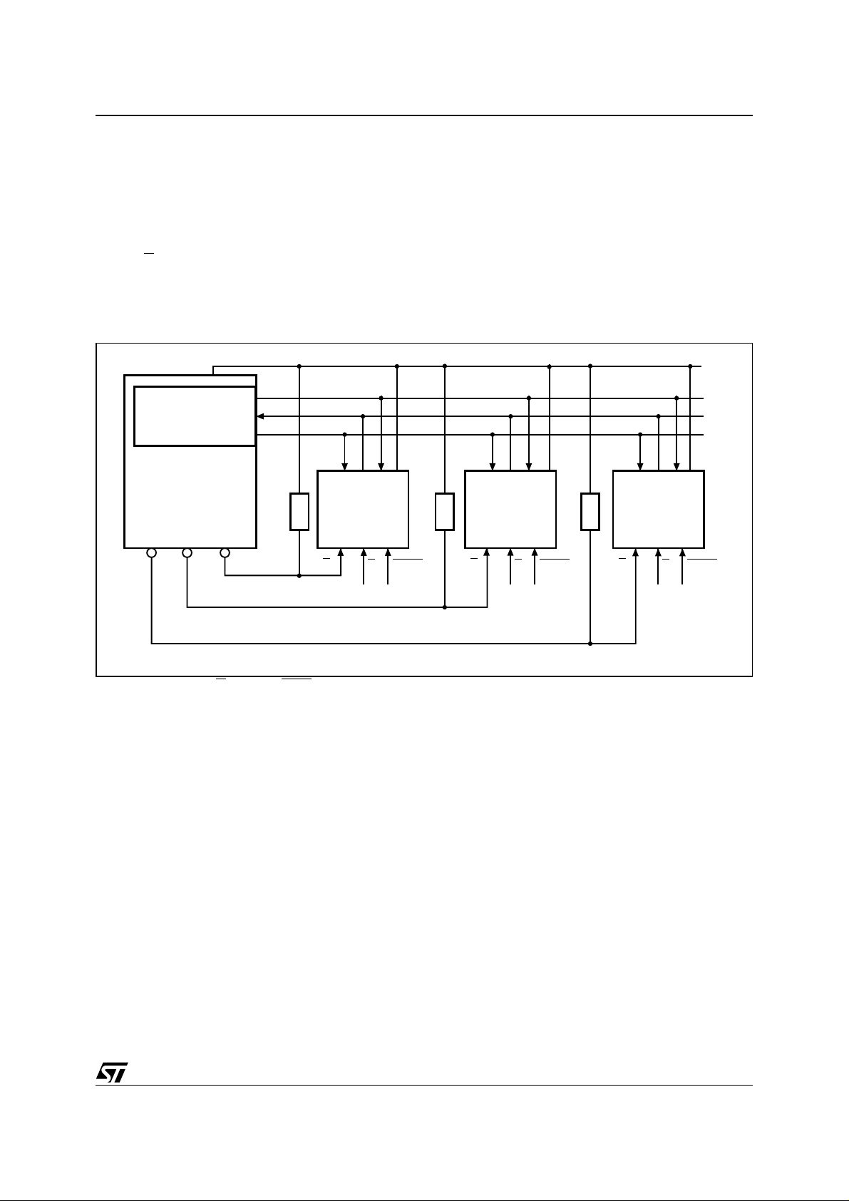
Figure 4. Bus Master and Memory Devices on the SPI Bus
SPI Interface with
(CPOL, CPHA) =
(0, 0) or (1, 1)
Bus Master
(ST6, ST7, ST9,
ST10, Others)
CS3 CS2 CS1
SDO
SDI
SCK
CQD
RRR
SPI Memory
Device
(Q) is latched on the first fa ll ing edge of the Serial
Clock (C) after the instruct ion (such as the Read
from Memory Array and Read S tatus Register in structions) have been clocked into the device.
Figure 4. shows three devices, connected to an
MCU, on a SPI bus. Only one device is selected at
a time, so only one device drives the S erial Data
Output (Q) line at a tim e, a ll th e others being high
impedance.
V
CC
CQD
SPI Memory
Device
M95640, M95320
V
CC
V
CC
CQD
SPI Memory
Device
V
CC
S
Note: The Write Protect (W) and Hold (HOLD) signals should be driven, High or Low as appropriat e.
HOLD
W
S
HOLD
W
S
W
AI03746e
HOLD
7/42

M95640, M95320
SPI Modes
These devices ca n be driv en by a m icrocontr oller
with its SPI peripheral runnin g in either of the two
following modes:
– CPOL=0, CPHA=0
– CPOL=1, CPHA=1
For these two modes, inpu t data is latched in on
the rising edge of Serial Clock (C), and output data
Figure 5. SPI Modes Supported
CPHA
CPOL
0
0
1
1
C
C
D
Q
MSB
is available from the falling edge of Serial Clock
(C).
The difference between the two modes, as shown
in Figure 5., is the clock polarity when the bus
master is in Stan d-by mode and not transferring
data:
– C remains at 0 for (CPOL=0, CPHA=0)
– C remains at 1 for (CPOL=1, CPHA=1)
MSB
AI01438B
8/42

OPERATING FEATURES
Power-Up
When the power supply is turned on, V
from V
During this time, the Ch ip Select (S
lowed to follow the V
to VCC.
SS
) must be al-
voltage. It must not be al-
CC
lowed to float, but should be connected to V
a suitable pull-up resistor.
As a built in safety feature, Chip Select (S
sensitive as well as level sensitive. After Powerup, the device does not become selected until a
falling edge has first been detected on Chip Select
(S
). This ensures that Chip Select (S) must have
been High, prior to going Low to star t the first operation.
Power On Reset: V
Lock-Out Write Protect
CC
In order to prevent inadvertent Write operations
during Power-up, each device include a Power On
Reset (POR) circuit. At Power-up, the dev ice will
not respond to any instruction until V
reached the Power On Reset threshold voltage.
This threshold is lower than the V
min operating
CC
voltage defined in Tables 10, 11, 12 and 13.
Similarly, as soon as V
drops from the normal
CC
operating voltage, below the Power On Reset
threshold voltage, the dev ice stops respondi ng to
any instruction sent to it.
Prior to selecting and issuing instructions to the
memory, a valid stable V
voltage must be ap-
CC
plied. This voltage must remain stable and valid
until the end of the transmissi on of the instruc tion
and, for a Write in struction, until the complet ion o
the internal write cycle (t
).
W
Power-down
At Power-down, the device must be deselected.
Chip Select (S
voltage applied on V
) should be allowed to follow the
.
CC
rises
CC
via
CC
) is edge
has
CC
M95640, M95320
Active Power and Standby Power Modes
When Chip Select (S
ed, and in the Active Power mode. The device
consumes I
CC
20..
When Chip Sel ec t (S
lected. If an Erase/Writ e cycle is not currently in
progress, the device then goe s in to the Standby
Power mode, and the device consump tion drops
to I
.
CC1
Hold Condition
The Hold ( HO LD
rial communications with the device without resetting the clocking sequence.
During the Hold condition, the S erial Data Output
(Q) is high impedance, and Serial Data Input (D )
and Serial Clock (C) are Don’t Care.
To enter the Hold condition, th e device must be
selected, with Chip Select (S
Normally, th e device i s kept sele cted, for the whole
duration of the Hold condition. Deselecting the device while it is in the Hold condition, has the effect
of resetting the state of the device, and this mechanism can be us ed if it is req uired to reset any pr ocesses that had been in progress.
The Hold condition starts when the Hol d (HOLD
signal is driven Low at the same time as Serial
Clock (C) already being Low (as shown in Figure
6.).
The Hold condition ends wh en the Hold (HOLD
signal is driven High at the same time as Serial
Clock (C) already being Low.
Figure 6. also shows what happens if the rising
and falling edges are not timed to coincide with
Serial Clock (C) being Low.
) is Low, the device is se lec t-
, as specified in Tabl e 16. to Table
) is High, the d ev ice is de se -
) signal is used to pau se a ny se -
) Low.
)
)
9/42

M95640, M95320
Figure 6. Hold Condition Activation
C
HOLD
Hold
Condition
Status Register
Figure 7. shows the position of the Status Register
in the control logic of the device. The Statu s Register contains a number of status and co ntrol bits
that can be read or set (as appropriate) by specific
instructions.
WIP bit. The Write In Progress (WIP) bit indicates
whether the memory is busy with a Write or Write
Status Register cycle.
WEL bit. The Write Enable Latch (WE L) bit indicates the status of the internal Write Enable Latch.
BP1, BP0 bits. The Block Protect (BP1, BP0) bits
are non-volatile. They define the size of the area to
be software protected against Write instructions.
SRWD bit. The Status Register Write Disable
(SRWD) bit is operated in conjunction with the
Write Protect (W
) signal. The Status Register
Write Disable (SRWD) bi t and Write Protect (W
signal allow the device to b e put in the Hardware
Protected mode. In this mode, the non-volatile bits
of the Status Register (SRWD, BP1, BP0) become
read-only bits.
Table 4. Status Register Format
b7 b0
SRWD 0 0 0 BP1 BP0 WEL WIP
Status Register Write Protect
Block Protect Bits
Write Enable Latch Bit
Write In Progress Bit
Hold
Condition
Data Protection and Protocol Control
Non-volatile memory devices can be used in environments that are particularly noisy, and within applications that could experience problems if
memory bytes are corrupted. Consequently, the
device features the following data protection
mechanisms:
■ Write and Write Status Register instructions
are checked that they consist of a number of
clock pulses that is a multiple of eight, before
they are accepted for execution.
■ All instructions that modify data must be
preceded by a Write Enable (WREN)
instruction to set the Write Enable Latch
(WEL) bit. This bit is returned to its reset state
by the following events:
– Power-up
)
– Write Disable (WRDI) instruction
completion
– Write Status Register (WRSR) instruction
completion
– Write (WRITE) instruction completion
■ The Block Protect (BP1, BP0) bits allow part of
the memory to be configured as read-only.
This is the Software Protected Mode (SPM).
■ The Write Protect (W) signal allows the Block
Protect (BP1, BP0) bits to be protected. This is
the Hardware Protected Mode (HPM).
For any instruction to be accepted, and executed,
Chip Select (S
) must be driven High after the rising
edge of Serial Clock (C) for the last bit of the instruction, and before the next rising edge of Serial
Clock (C).
Two points need to be noted in the previous sentence:
AI02029D
10/42

M95640, M95320
– The ‘last bit of the instruction’ can be the
eighth bit of the instruction code, or the eighth
bit of a data byte, depending on the instruction
– The ‘next rising edge of Serial Clock (C)’ might
(or might not) be the next bus transaction for
some other device on the SPI bus.
(except for Read Status Register (RDSR) and
Read (READ) instructions).
Table 5. Write-Protected Block Size
Status Register Bits
BP1 BP0
Protected Block
0 0 none none none
0 1 Upper quarter 1800h - 1FFFh 0C00h - 0FFFh
1 0 Upper half 1000h - 1FFFh 0800h - 0FFFh
1 1 Whole memory 0000h - 1FFFh 0000h - 0FFFh
M95640, M95640-W,
M95640-R, M95640-S
Array Addresses Protected
M95320, M95320-W,
M95320-R, M95320-S
11/42

M95640, M95320
MEMORY ORGANIZATION
The memory is organized as shown in Figure 7..
Figure 7. Block Diagram
HOLD
W
S
C
D
Q
Control Logic
I/O Shift Register
Address Register
and Counter
Y Decoder
High Voltage
Generator
Data
Register
1 Page
Status
Register
Size of the
Read only
EEPROM
area
12/42
X Decoder
AI01272C

INSTRUCTIONS
Each instruction star ts wi th a singl e- by te cod e, a s
summarized in Table 6..
If an invalid instruct ion is sent ( one not contain ed
in Table 6.), the device automaticall y des elect s it self.
M95640, M95320
Table 6. Instruction Set
Instruc
tion
WREN Write Enable 0000 0110
WRDI Write Disable 0000 0100
RDSR Read Status Register 0000 0101
WRSR Write Status Register 0000 0001
READ Read from Memory Array 0000 0011
WRITE Write to Memory Array 0000 0010
Description
Instruction
Format
13/42

M95640, M95320
Write Enable (WREN)
The Write Enable Latch (WEL) bit must be set prior to each WRITE and WRSR instruction. The only
way to do this is to send a Write Enable instruction
to the device.
Figure 8. Write Enable (WREN) Sequence
S
0
C
D
High Impedance
Q
Write Disable (WRDI)
One way of resetting the Write Enable Latch
(WEL) bit is to send a Write Disable in struction to
the device.
As shown in Fi gure 9., to send this instruction to
the device, Chip Select (S
) is driven Low, and the
bits of the instruc tion by te a r e shi fted i n, o n S er ial
Data Input (D).
As shown in Figu re 8., to send this instructio n to
the device, Chip Select (S
) is driven Low, and the
bits of the instruc tion by te a r e s hifted i n, o n S er ial
Data Input (D). The device then enters a wait
state. It waits for a the device to be deselected, by
Chip Select (S
21 34567
Instruction
) being driven High.
AI02281E
The device then e nters a wait state. It waits for a
the device to be deselected, by Chip Select (S
ing driven High.
The Write Enable Latch (WEL) bit, in fact, becomes reset by any of the following events:
– Power-up
– WRDI instruction execution
– WRSR instruction completion
– WRITE instruction completion.
) be-
Figure 9. Write Disable (WRDI) Sequence
S
C
D
High Impedance
Q
14/42
0
21 34567
Instruction
AI03750D

M95640, M95320
Read Status Register (RDSR)
The Read Status Register (RDSR) instruction allows the Status Register to be read. The Status
Register may be read at any time, even while a
Write or Write Status Register cycle is in progress.
When one of these c ycles is in p rogr ess, it is r ecommended to check the Write In Progress (WIP)
bit before sending a new instruction to the device.
It is also possible to read the Status Register continuously, as shown in Figure 10..
The status and control bits o f the Status Regi ster
are as follows:
WIP bit. The Write In Progress (WIP) bit indicates
whether the memory is busy with a Write or Write
Status Register cycle. When set to 1, such a cycle
is in progress, whe n rese t to 0 no such cyc le is in
progress.
WEL bit. The Write Enable Latch (WE L) bit indicates the status of the internal Write Enable Latch.
When set to 1 the inte rnal Write Enable Latch is
set, when set to 0 the inter nal W rite Ena ble Latc h
is reset and no Writ e or Write Status Register instruction is accepted.
Figure 10. Read Status Register (RDSR) Sequence
BP1, BP0 bits. The Block Protect (BP1, BP0) bits
are non-volatile. They define the size of the area to
be software protected agains t Write instructions.
These bits are written with the Write Status Register (WRSR) instruction. When one or both of the
Block Protect (BP1, BP 0) bit s is set to 1, th e rele vant memory area (as defined in Table 4.) becomes protected against Write (WRITE)
instructions. The Block Protect (BP1, BP0) bits
can be written provided that the Hardware Protected mode has not been set.
SRWD bit. The Status Register Write Disable
(SRWD) bit is operated in conjunction with the
Write Protect (W
) signal. The Status Register
Write Disable (SRWD) bi t and Write Protect (W
signal allow the device t o be put in the Hardwar e
Protected mode (when the Status Register Write
Disable (SRWD) bit is set to 1, and Writ e Protect
(W
) is driven Low). In this mode, the non-vol atile
bits of the Status Register (SRWD, BP1, BP0) become read-only bits and the Write Status Register
(WRSR) instruction is no longer accepted for execution.
)
S
21 3456789101112131415
0
C
Instruction
D
Q
High Impedance
Status Register Out
7 6543210
MSB
Status Register Out
7 6543210
MSB
7
AI02031E
15/42

M95640, M95320
Write Status Register (WRSR)
The Write Status Register (WRSR ) instructi on allows new values to be written to the Status Register. Before it can be accepted, a Write Enable
(WREN) instruction must previously have been executed. After the Write Enable (WREN) instruction
has been decoded and executed, the device se ts
the Write Enable Latch (WEL).
The Write Status Register ( WRSR) instruction is
entered by drivin g Chip Select (S
) Low, followed
by the instruction code and the data byte on Serial
Data Input (D).
The instruction sequence is shown in F i gure 11..
The Write Status Register (WRSR) instruction has
no effect on b6, b5, b4, b1 and b0 of the S tatus
Register. b6, b5 and b4 are always read as 0.
Chip Select (S
) must be driven High after the rising
edge of Serial Cloc k (C) that latch es in th e eig hth
bit of the data byte, and before the next rising edge
of Serial Clock (C). Otherwise, the Write Status
Register (WRSR) instruc tion is not executed. As
soon as Chip Select (S
) is driven High, the self-
timed Write Status Register cycle (whose duration
) is initiated. Wh ile the Write Status R egister
is t
W
cycle is in progres s, the Status Register ma y still
be read to check the value of the Write In Progress
(WIP) bit. The Write In Progress (WIP) bit is 1 during the self-timed Write Status Register cycle, and
is 0 when it is completed. W hen the cy cle is completed, the Write Enable Latch (WEL) is reset.
The Write Status Register (W RSR) instruction al lows the user to change t he values of the Block
Protect (BP1, BP0) bits, to defin e the size of the
area that is to be treated as r ead-o nly, as de fined
in Table 4..
The Write Status Register (WRSR) instruction also
allows the user to s et o r res et t he Sta tus Re gi ste r
Write Disable (SRWD) bi t in accordance with the
Write Protect (W
) signal. The Status Register
Write Disable (SRWD) bi t and Write Protect (W
signal allow the device t o be put in the Hardwar e
Protected Mode (HPM). The Write Status Register
(WRSR) instruction is not executed once the Hardware Protected Mode (HPM) is entered.
The contents of the Sta tus Reg ister W rite Dis ab le
(SRWD) and Block Protect (BP1, BP0) bits are frozen at their current values from just before the
start of the execution of Write Status Register
(WRSR) instruction. The new, updated, values
take effect at the moment of completion of the execution of Write Sta tus Register (W RSR) instruction.
)
Table 7. Protection Modes
W
Signal
Note: 1. As defined by the values in the Block Protect (BP1, BP0) bits of the Status Register, as shown in Table 5..
SRWD
Bit
10
00
11
01
Mode
Software
Protected
(SPM)
Hardware
Protected
(HPM)
The protection feature s of the de vice are summa rized in Tab le 5..
When the Status Regis ter Write Disable (S RWD)
bit of the Status Register is 0 (its initial delivery
state), it is possible to wr it e to the S tatu s Regi ste r
provided that the Write Enable Latch (WEL) bit has
previously been set by a Write Enable (WREN) instruction, regardles s of the whethe r Write Pr otect
(W
) is driven High or Low.
When the Status Regis ter Write Disable (S RWD)
bit of the Status Register is set to 1, two cases
need to be considered, depen ding on the sta te of
Write Protect (W
):
Write Protection of the
Status Register
Status Register is Writable
(if the WREN instruction
has set the WEL bit)
The values in the BP1 and
BP0 bits can be changed
Status Register is
Hardware write protec te d
The values in the BP1 and
BP0 bits cannot be
changed
Protected Area
Write Protected
Write Protected
– If Write Protect (W
possible to write to the Status Register
provided that the Write Enable Latch (WEL) bit
has previously been set by a Write Enable
(WREN) instruction.
– If Write Protect (W
possible to write to the Status Register
the Write Enable Latch (WEL) bit has
previously been set by a Write Enable
(WREN) instruction. (Attempts to write to the
Status Register are rejected, and are not
accepted for execution). As a consequence,
all the data bytes in the memory area that are
software protected (SPM) by the Block Protect
Memory Content
1
Unprotected Area
Ready to accept Write
instructions
Ready to accept Write
instructions
) is driven High, it is
) is driven Low, it is
1
not
even
if
16/42

M95640, M95320
(BP1, BP0) bits of the Status Register, are
also hardware protected against data
modification.
Regardless of the order of the two events, the
Hardware Protected Mode (HPM) can be entered:
– by setting the Status Register Write Disable
(SRWD) bit after driving Write Protect (W
– or by driving Write Protect (W
) Low after
) Low
setting the Status Register Write Disable
(SRWD) bit.
The only way to exit the Hardware Protected Mode
(HPM) once entered is to pull Write Protect (W
)
High.
Figure 11. Write Status Register (WRSR) Sequence
S
21 3456789101112131415
0
C
Instruction Status
If Write Protect (W
) is permanently tie d High, the
Hardware Protected Mode (HPM) can never be
activated, and only the S oftware Protected Mode
(SPM), using the Block Prote ct (BP1, BP 0) bits of
the Status Register, can be used.
Table 8. Address Range Bits
Device
Address Bits A12-A0 A11-A0
Note: b15 to b13 are Don’t Care on the 64 Kbit devices.
b15 to b12 are Don’t Care on the 32 Kbit devices.
Register In
32 Kbit
Devices
64 Kbit
Devices
D
High Impedance
Q
765432 0
MSB
1
AI02282D
17/42

M95640, M95320
Read from Memory Array (READ)
As shown in Figure 12., to send this instr uction to
the device, Chip Select (S
) is first driven Low. The
bits of the instruction by te and address by tes are
then shifted in, on Serial Data Input (D). The ad dress is loaded into an internal addre ss register,
and the byte of data at that addres s i s shi fted out,
on Serial Data Output (Q).
If Chip Select (S
) continues to be driven Low, the
internal address register is automatically incremented, and the byte of data at the new address is
shifted out.
When the highest address is reached, the address
counter rolls over to zero, allowing the Read cycle
to be continued indefinitely. The whole memory
can, therefore, be read with a single READ instruction.
The Read cycle is termin ated b y drivin g Chip Se lect (S
(S
The first byte addr essed can be any byte within
any page.
The instruction is not accepted, and is not executed, if a Write cycle is currently in progress.
Figure 12. Read from Memory Array (READ) Sequence
S
21 345678910 2021222324252627
0
C
Instruction 16-Bit Address
15
D
High Impedance
Q
1413 3210
MSB
) High. The rising edg e of the Chip Select
) signal can occur at any time during the cycle.
28 29 30
Data Out 1
76543 1 7
MSB
31
Data Out 2
2
0
AI01793D
Note: Depending on the memory size, as shown in Table 8., the most significant address bits are Don’t Care.
18/42

M95640, M95320
Write to Memory Array (WRITE)
As shown in Figure 13., to send this instr uction to
the device, Chip Select (S
) is first driven Low. The
bits of the instruction b yte, address byte, and at
least one data byte are then shifted in, on Serial
Data Input (D).
The instruction is terminated by driving Chip Select (S
) High at a byte boundary of the input da ta.
In the case of Figure 13., this occurs after the
eighth bit of the data byte has been latched in, indicating that the instruction is being used to write
a single byte. The self-timed Write cycle starts,
and continues for a period t
(as specified in Ta-
WC
ble 22. to Table 26. ), at the end of which the Write
in Progress (WIP) bit is reset to 0.
If, though, Chip Select (S
) continues to be driven
Low, as shown in Figure 14., the next byte of input
data is shifted in, s o that m ore th an a sing le by te,
starting from the given address towards the end of
the same page, ca n be w ritten in a sin gle i ntern al
Write cycle.
Figure 13. Byte Write (WRITE) Sequence
Each time a new data byte i s shifted in, the lea st
significant bits o f the i ntern al ad dress count er ar e
incremented. If the number of data bytes sent to
the device exceeds t he page boundary, th e internal address counter rol ls over to the beg inning of
the page, and the previous data there are overwritten with the incoming data. (The page size of
these device s is 32 bytes).
The instruction is not accepted, and is not executed, under the following conditions :
– if the Write Enable Latch (WEL) bit has not
been set to 1 (by executing a Write Enable
instruction just before)
– if a Write cycle is already in progress
– if the device has not been deselected, by Chip
Select (S
) being driven High, at a byte
boundary (after the eighth bit, b0, of the last
data byte that has been latched in)
– if the addressed page is in the region
protected by the Block Protect (BP1 and BP0)
bits.
S
21 345678910 2021222324252627
0
C
Instruction 16-Bit Address
15
D
High Impedance
Q
Note: Depending on the memory size, as shown in Table 8., the most significant address bits are Don’t Care.
1413 3210
765432 0
28 29 30
Data Byte
31
1
AI01795D
19/42

M95640, M95320
Figure 14. Page Write (WRITE) Sequence
S
21 345678910 2021222324252627
0
C
28 29 30
31
Instruction 16-Bit Address
15
D
S
3433 35 36 37 38 39 40 41 42 44 45 46 4732
C
Data Byte 2
D
Note: Depending on the memory size, as shown in Table 8., the most significant address bits are Don’t Care.
765432 0
1
1413 3210
43
Data Byte 3
765432 0
1
765432 0
Data Byte 1
Data Byte N
65432 0
1
1
AI01796D
20/42

POWER-UP AND DELIVERY STATE
Power-up State
After Power-up, the device is in the following state:
– Standby Power mode
– deselected (after Power-up, a falling edge is
required on Chip Select (S
instructions can be started).
– not in the Hold Condition
– the Write Enable Latch (WEL) is reset to 0
– Write In Progress (WIP) is reset to 0
) before any
M95640, M95320
The SRWD, BP1 and BP0 bi ts of th e Status Register are unchanged from the previous powerdown (they are non-volatile bits).
INITIAL DELIVERY STATE
The device is delivered with the memory array set
at all 1s (FFh). The Sta tus Regis ter Wr ite Dis able
(SRWD) and Block Protect (BP1 and BP0) bits are
initialized to 0.
21/42

M95640, M95320
MAXIMUM RATING
Stressing the devi ce outside the ratings li sted in
Table 9. may cause permanent damage to the de-
vice. These are stress ratings only, and oper ation
of the device at these, or any other conditions outside those indicated in the Oper ating sections of
Table 9. Absolute Maximum Ratings
Symbol Parameter Min. Max. Unit
T
STG
T
LEAD
V
O
V
I
V
CC
V
ESD
Note: 1. Compliant with JEDEC Std J-STD-020C (for small body, Sn-Pb or Pb assembly), the ST ECOPACK® 7191395 specification, and
the European directive on Restrictions on Hazardous Substances (RoHS) 2002/ 95/EU
2. AEC-Q100-002 (compliant with JEDEC Std JESD22-A114A, C1=100pF, R1=1500Ω, R2=500Ω)
Storage Temp era tur e –65 150 °C
Lead Temperature during Soldering
Output Voltage –0.50
Input Voltage –0.50 6.5 V
Supply Voltage –0.50 6.5 V
Electrostatic Discharg e Voltage (Human Body mode l)
this specificatio n, is not implied. Exposure to Absolute Maximum Rating conditions for extended
periods may affect de vice rel iability. Refer also to
the STMicroelectroni cs SURE Program and othe r
relevant quality documents.
See note
2
–4000 4000 V
1
V
+0.6
CC
°C
V
22/42

M95640, M95320
DC AND AC PARAMETERS
This section summ arizes the operati ng and measurement conditions , and the D C an d AC charac teristics of the device. The parameters in th e DC
and AC Characteristic tables that follow are derived from tests performed under the Measure-
Table 10. Operating Conditions (M95320 and M95640)
Symbol Parameter Min. Max. Unit
ment Conditions summarized in the relevant
tables. Designers sho uld c heck tha t th e operating
conditions in thei r circui t match the measur ement
conditions when relying on the quoted parameters.
V
CC
Supply Voltage 4.5 5.5 V
Ambient Operating Temperature (Device Grade 6) –40 85 °C
T
A
Ambient Operating Temperature (Device Grade 3) –40 125 °C
Table 11. Operating Conditions (M95320-W and M95640-W)
Symbol Parameter Min. Max. Unit
V
CC
Supply Voltage 2.5 5.5 V
Ambient Operating Temperature (Device Grade 6) –40 85 °C
T
A
Ambient Operating Temperature (Device Grade 3) –40 125 °C
Table 12. Operating Conditions (M95320-R and M95640-R)
Symbol
V
CC
T
A
Note: 1. This product is under development. For more information, please contact your nearest ST sales offi ce.
Supply Voltage 1.8 5.5 V
Ambient Operating Temperature –40 85 °C
Parameter Min.
1
Max.
1
Table 13. Operating Conditions (M95320-S and M95640-S)
Symbol
Parameter Min.
1
Max.
1
Unit
Unit
V
CC
T
A
Note: 1. This product is under development. For more information, please contact your nearest ST sales offi ce.
Supply Voltage 1.65 5.5 V
Ambient Operating Temperature –40 85 °C
Table 14. AC Measurement Conditions
Symbol Parameter Min. Typ. Max. Unit
C
L
Note: Output Hi-Z is defined as the point where data out is no longer driven.
Load Capacitance 30 pF
Input Rise and Fall Times 50 ns
0.2V
0.3V
to 0.8V
CC
to 0.7V
CC
CC
CC
Input Pulse Voltages
Input and Output Timing Reference Voltages
V
V
23/42

M95640, M95320
Figure 15. AC Measurement I/O Waveform
Input Levels
0.8V
CC
0.2V
CC
Input and Output
Timing Reference Levels
0.7V
CC
0.3V
CC
AI00825B
Table 15. Capacitance
Symbol Parameter Test Condition Min. Max. Unit
C
OUT
C
IN
Output Capacitanc e (Q) V
Input Capacitance (D) VIN = 0V 8 pF
Input Capacitance (other pins) V
Note: Sampled only, not 100% tested, at TA=25°C and a frequency of 5MHz.
= 0V 8 pF
OUT
= 0V 6 pF
IN
Table 16. DC Characteristics (M95320 and M95640, Device Grade 6)
Symbol Parameter Test Condition Min. Max. Unit
I
I
I
CC1
I
Input Leakage Current
LI
Output Leakage Current
LO
Supply Current
CC
Supply Current
(Standby)
V
CC
V
CC
V
IN
V
IN
V
V
V
V
V
OH
Note: 1. For all 5V range devices, the device meets the output requirements for both TTL and CMOS standards.
Input Low Voltage –0.45
IL
Input High Voltage 0.7 V
IH
1
Output Low Voltage
OL
1
Output High Voltage IOH = –2 mA, VCC = 5V 0.8 V
2. Previous product version is identified by Process Identifica tion letter ‘S’.
3. Current product version is identified by Process Identification letter ‘V’’.
4. New product version is identified by Process Identification letter ‘P’.
5. Preliminary data.
V
= VSS or V
IN
S
= VCC, V
C = 0.1V
= 5V, Q = open,
V
CC
Previous Product
C=0.1V
CC
OUT
/0.9VCC at 5MHz,
CC
/0.9VCC at 10MHz,
CC
= VSS or V
2
CC
= 5V, Q= open, Current Product
C=0.1V
/0.9VCC at 20MHz,
CC
= 5V, Q = open, New Product
= VCC, V
S
CC
= 5V,
= VSS or VCC, Previous Product
= V
, V
S
CC
CC
= 5V,
= VSS or VCC, Current Product
= VCC, V
S
= VSS or VCC, New Product
IN
I
= 2 mA, VCC = 5V
OL
CC
= 5V,
4,5
4,5
3
± 2 µA
± 2 µA
4mA
3
5mA
10
2
10 µA
2µA
2µA
0.3 V
CC
VCC+1 V
CC
0.4 V
CC
mA
V
V
24/42

M95640, M95320
Table 17. DC Characteristics (M95320 and M95640, Device Grade 3)
Symbol Parameter Test Condition Min. Max. Unit
I
I
I
CC1
I
Input Leakage Current
LI
Output Leakage Current
LO
Supply Current
CC
Supply Current
(Standby)
V
CC
V
CC
V
CC
V
IN
V
IN
V
V
V
V
V
OH
Note: 1. For all 5V range devices, the device meets the output requirements for both TTL and CMOS standards.
Input Low Voltage –0.45
IL
Input High Voltage
IH
1
Output Low Voltage IOL = 2mA, VCC = 5V 0.4 V
OL
1
Output High Voltage
2. Previous product version is identified by Process Identifica tion letter ‘S’.
3. Current product version is identified by Process Identification letters ‘B’.
4. New product version is identified by Process Identification letters ‘P’.
5. Preliminary data.
V
= VSS or V
S
= VCC, V
C = 0.1V
IN
OUT
/0.9VCC at 2MHz,
CC
CC
= VSS or V
CC
= 5V, Q = open, Previous Product
C = 0.1V
/0.9VCC at 5MHz,
CC
= 5V, Q= open, Current Product
C=0.1V
= 5V, Q = open, New Product
/0.9VCC at 20MHz,
CC
= V
CC
, V
S
CC
4,5
= 5V,
= VSS or VCC, Previous Product
= VCC, V
S
= VSS or VCC, Current Product
S
= V
= VSS or VCC, New Product
IN
I
= –2mA, VCC = 5V 0.8 V
OH
CC
, V
CC
CC
= 5V,
3
= 5V,
4,5
± 2 µA
± 2 µA
2
3
2mA
4mA
12
2
20 µA
5µA
2µA
0.3 V
CC
0.7 V
CC
CC
VCC+1
mA
V
V
V
25/42

M95640, M95320
Table 18. DC Characteristics (M95320-W and M95640-W, Device Grade 6)
Symbol Parameter Test Condition Min. Max. Unit
I
I
I
CC1
I
Input Leakage Current
LI
Output Leakage Current
LO
Supply Current
CC
Supply Current
(Standby)
= 2.5V, Q = open, Previous Product
V
CC
= 2.5V, Q = open, Current Product
V
CC
V
CC
V
IN
V
IN
V
V
V
V
V
Note: 1. Previous product version is identified by Process Identificatio n letter ‘S’.
Input Low Voltage –0.45
IL
Input High Voltage
IH
Output Low Voltage
OL
Output High Voltage
OH
2. Current product version is identified by Process Identification letter ‘V’’.
3. New product version is identified by Process Identification letter ‘P’.
4. Preliminary data.
V
= VSS or V
IN
S
= VCC, V
C = 0.1V
C = 0.1V
C=0.1V
OUT
/0.9VCC at 2MHz,
CC
/0.9VCC at 5MHz,
CC
/0.9VCC at 10MHz,
CC
= 2.5V, Q = open, New Product
= VCC, V
S
= VSS or VCC, Previous Product
= VCC, V
S
= VSS or VCC, Current Product
S
= VCC, V
= VSS or VCC, New Product
IN
I
= 1.5mA, VCC = 2.5V
OL
I
= –0.4mA, VCC = 2.5V 0.8 V
OH
CC
= VSS or V
= 2.5V,
CC
= 2.5V
CC
= 2.5V
CC
CC
1
2
3,4
1
2
3,4
0.7 V
CC
CC
± 2 µA
± 2 µA
2mA
3mA
5
2µA
1µA
1
0.3 V
CC
VCC+1
0.4 V
mA
µA
V
V
V
Table 19. DC Characteristics (M95320-W and M95640-W, Device Grade 3)
Symbol Parameter Test Condition
I
I
I
I
CC1
V
V
V
V
Note: 1. Current product version is identified by Process Identification letter ‘B’.
Input Leakage Current V
LI
Output Leakage Current
LO
S
C = 0.1V
V
= 2.5V, Q = open, Current Product
Supply Current
CC
Supply Current (Standby)
Input Low Voltage –0.45
IL
Input High Voltage
IH
Output Low Voltage
OL
Output High Voltage
OH
2. New product version is identified by Process Identification letter ‘P’.
CC
C=0.1V
V
= 2.5V, Q = open, New Product
CC
S
= VCC, V
I
OH
= VSS or V
IN
= VCC, V
I
OL
OUT
/0.9VCC at 5MHz,
CC
/0.9VCC at 10MHz,
CC
= 2.5V, V
CC
= 1.5mA, VCC = 2.5V
CC
= VSS or V
= VSS or V
IN
CC
= –0.4mA, VCC = 2.5V 0.8 V
1
2
CC
Min.
0.7 V
CC
CC
Max. Unit
± 2 µA
± 2 µA
3mA
6mA
2µA
0.3 V
VCC+1
CC
V
V
0.4 V
V
26/42

Table 20. DC Characteristics (M95320-R and M95640-R)
Symbol Parameter
I
I
I
I
CC1
V
V
V
V
Note: 1. This product is under qualification. For more information, pleas e contact your nearest ST sales office .
Input Leakage Current
LI
Output Leakage Current
LO
Supply Current
CC
S
Supply Current (Standby)
Input Low Voltage –0.45
IL
Input High Voltage
IH
Output Low Voltage
OL
Output High Voltage
OH
2. Preliminary data.
= VCC, V
Test Condition Min.
= VSS or V
V
IN
S
= VCC, V
C = 0.1V
V
I
= 0.15 mA, VCC = 1.8 V
OL
I
= –0.1 mA, VCC = 1.8 V 0.8 V
OH
OUT
/0.9VCC at 5MHz,
CC
= 1.8 V, Q = open
CC
= VSS or VCC, V
IN
CC
= VSS or V
CC
CC
= 1.8V
0.7 V
Table 21. DC Characteristics (M95320-S and M95640-S)
Symbol Parameter
I
Input Leakage Current V
LI
I
Output Leakage Current
LO
I
Supply Current
CC
S
I
V
V
Note: 1. This product is under qualification. For more information, pleas e contact your nearest ST sales office .
Supply Curre nt (Standby)
CC1
V
Input Low Voltage –0.45
IL
V
Input High Voltage 0.7 V
IH
Output Low Voltage
OL
Output High Voltage
OH
2. Preliminary data.
= VCC, V
Test Condition Min.
= VSS or V
IN
S
= VCC, V
C = 0.1V
V
I
= 0.15 mA, VCC = 1.65V
OL
I
= –0.1 mA, VCC = 1.65V 0.8 V
OH
OUT
/0.9VCC at 2MHz,
CC
= 1.6 5 V, Q = open
CC
= VSS or VCC, V
IN
CC
= VSS or V
CC
CC
= 1.65V
1,2
CC
CC
M95640, M95320
1,2
CC
CC
1,2
Max.
± 1 µA
± 1 µA
3mA
1µA
0.3 V
CC
VCC+1
0.3 V
1,2
Max.
± 1 µA
± 1 µA
1mA
1µA
0.3 V
CC
VCC+1 V
0.3 V
Unit
V
V
V
Unit
V
V
27/42

M95640, M95320
Table 22. AC Characteristics (M95320 and M95640, Device Grade 6)
Test conditions specified in Table 14. and Table 10.
Previous
Product
Symbol Alt. Parameter
Version
Min. Max. Min. Max. Min. Max.
f
f
C
t
SLCHtCSS1
t
SHCHtCSS2
t
SHSLtCS
t
CHSHtCSH
t
CHSL
1
t
CH
1
t
CL
2
t
CLCH
2
t
CHCL
t
DVCHtDSU
t
CHDXtDH
t
HHCH
t
HLCH
t
CLHL
t
CLHH
2
t
SHQZ
t
CLQV
t
CLQXtHO
2
t
QLQH
2
t
QHQL
t
HHQVtLZ
2
t
HLQZ
t
W
Note: 1. tCH + tCL must never be lower than the shortes t possible clock period, 1/fC(max).
2. Value guaranteed by characterization, not 10 0% t ested in production.
3. Previous product version is identified by Process Identifica tion letter ‘S’.
4. Current product version is identified by Process Identification letter ‘V’’.
5. New product version is identified by Process Identification letter ‘P’.
6. Preliminary Data.
Clock Frequency D.C. 5 D.C. 10 D.C. 20 MHz
SCK
S Active Setup Time 90 15 15 ns
S Not Active Setup Time 90 15 15 ns
S Deselect Time 100 40 20 ns
S Active Hold Time 90 25 15 ns
S Not Active Hold Time 90 15 15 ns
t
Clock High Time 90 40 20 ns
CLH
t
Clock Low Time 90 40 20 ns
CLL
t
Clock Rise Time 1 1 2 µs
RC
t
Clock Fall Time 1 1 2 µs
FC
Data In Setup Time 20 15 5 ns
Data In Hold Time 30 15 10 ns
Clock Low Hold Time after HOLD not Active 70 15 15 ns
Clock Low Hold Time after HOLD Active 40 20 15 ns
Clock Low Set-up Time before HOLD Active 0 0 0 ns
Clock Low Set-up Time before HOLD not
Active
t
Output Disable Time 100 25 20 ns
DIS
t
Clock Low to Output Valid 60 25 20 ns
V
000ns
Output Hold Time 0 0 0 ns
t
Output Rise Time 50 20 20 ns
RO
t
Output Fall Time 50 20 20 ns
FO
HOLD High to Output Valid 50 25 20 ns
t
HOLD Low to Output High-Z 100 25 20 ns
HZ
t
Write Time 10 5 5 ms
WC
3
Current
Product
Version
New Product
4
Version
5,6
Unit
28/42

Table 23. AC Characteristics (M95320 and M95640, Device Grade 3)
Test conditions specified in Table 14. and Table 10.
Previous
Symbol Alt. Parameter
Product
Version
3
Current
Product
Version
M95640, M95320
New
4
Product
Version
5,6
Unit
Min. Max.
f
t
SLCHtCSS1
t
SHCHtCSS2
t
SHSL
t
CHSHtCSH
t
CHSL
t
CH
t
CL
t
CLCH
t
CHCL
t
DVCHtDSU
t
CHDX
t
HHCH
t
HLCH
t
CLHL
t
CLHH
t
SHQZ
t
CLQV
t
CLQX
t
QLQH
t
QHQL
t
HHQV
t
HLQZ
t
W
Note: 1. tCH + tCL must never be lower than the shortes t possible clock period, 1/fC(max).
f
C
Clock Frequency D.C. 2 D.C. 5 D.C. 20 MHz
SCK
S Active Setup Time 200 90 15 n s
S Not Active Setup Time 200 90 15 ns
t
S Deselect Time 200 100 20 ns
CS
S Active Hold Time 200 90 15 ns
S Not Active Hold Time 200 90 15 ns
1
t
Clock High Time 200 90 20 ns
CLH
1
t
Clock Low Time 200 90 20 ns
CLL
2
t
Clock Rise Time 1 1 2 µs
RC
2
t
Clock Fall Time 1 1 2 µs
FC
Data In Setup Time 40 20 5 ns
t
Data In Hold Time 50 30 10 ns
DH
Clock Low Hold Time after HOLD not Active 140 70 15 ns
Clock Low Hold Time after HOLD Active 90 40 15 ns
Clock Low Set-up Time before HOLD Active 0 0 0 ns
Clock Low Set-up Time before HOLD not
Active
2
t
Output Disable Time 250 100 20 n s
DIS
t
Clock Low to Output Valid 150 60 20 ns
V
t
Output Hold Time 0 0 0 ns
HO
2
t
Output Rise Time 100 50 20 ns
RO
2
t
Output Fall Time 100 50 20 ns
FO
t
HOLD High to Output Valid 100 50 20 ns
LZ
2
t
HOLD Low to Output High-Z 250 100 20 ns
HZ
t
Write Time 10 5 5 m s
WC
2. Value guaranteed by characterization, not 10 0% t ested in production.
3. Previous product version is identified by Process Identifica tion letter ‘S’.
4. Current product version is identified by Process Identification letter ‘B’.
5. New product version is identified by Process Identification letter ‘P’.
6. Preliminary Data.
00 0ns
Min. Max. Min. Max.
29/42

M95640, M95320
Table 24. AC Characteristics (M95320-W and M95640-W, Device Grade 6)
Test conditions specified in Table 14. and Table 11.
Previous
Product
Symbol Alt. Parameter
Version
Min. Max. Min. Max. Min. Max.
f
f
C
t
SLCHtCSS1
t
SHCHtCSS2
t
SHSL
t
CHSHtCSH
t
CHSL
1
t
CH
1
t
CL
2
t
CLCH
2
t
CHCL
t
DVCHtDSU
t
CHDX
t
HHCH
t
HLCH
t
CLHL
t
CLHH
2
t
SHQZ
t
CLQV
t
CLQXtHO
2
t
QLQH
2
t
QHQL
t
HHQV
2
t
HLQZ
t
W
Note: 1. tCH + tCL must never be lower than the shortes t possible clock period, 1/fC(max).
2. Value guaranteed by characterization, not 10 0% t ested in production.
3. Previous product version is identified by Process Identifica tion letter ‘S’.
4. Current product version is identified by Process Identification letter ‘V’’.
5. New product version is identified by Process Identification letter ‘P’.
6. Preliminary Data.
Clock Frequency D.C. 2 D.C. 5 D.C. 10 MHz
SCK
S Active Setup Time 200 90 30 ns
S Not Active Setup Time 200 90 30 ns
t
S Deselect Time 200 100 40 ns
CS
S Active Hold Time 200 90 3 0 ns
S Not Active Hold Time 200 90 30 ns
t
Clock High Time 200 90 40 ns
CLH
t
Clock Low Time 200 90 40 ns
CLL
t
Clock Rise Time 1 1 2 µs
RC
t
Clock Fall Time 1 1 2 µs
FC
Data In Setup Time 40 20 10 ns
t
Data In Hold Time 50 30 10 ns
DH
Clock Low Hold Time after HOLD not Active 140 70 30 ns
Clock Low Hold Time after HOLD Active 90 40 30 ns
Clock Low Set-up Time before HOLD Active 0 0 0 ns
Clock Low Set-up Time before HOLD not
Active
t
Output Disable Time 250 100 40 ns
DIS
t
Clock Low to Output Valid 150 60 40 ns
V
000ns
Output Hold Time 0 0 0 ns
t
Output Rise Time 100 50 40 ns
RO
t
Output Fall Time 100 50 40 ns
FO
t
HOLD High to Output Valid 100 50 40 ns
LZ
t
HOLD Low to Output High-Z 250 100 40 ns
HZ
t
Write Time 10 5 5 ms
WC
Current
Product
3
Version
New
Product
4
Version
5,6
Unit
30/42

Table 25. AC Characteristics (M95320-W and M95640-W, Device Grade 3)
Test conditions specified in Table 14. and Table 11.
Current Product
Symbol Alt. Parameter
Version
Min. Max. Min. Max.
f
t
SLCHtCSS1
t
SHCHtCSS2
t
SHSL
t
CHSHtCSH
t
CHSL
t
CH
t
CL
t
CLCH
t
CHCL
t
DVCHtDSU
t
CHDX
t
HHCH
t
HLCH
t
CLHL
t
CLHH
t
SHQZ
t
CLQV
t
CLQX
t
QLQH
t
QHQL
t
HHQV
t
HLQZ
t
Note: 1. tCH + tCL must never be lower than the shortes t possible clock period, 1/fC(max).
f
C
Clock Frequency D.C. 5 D.C. 10 MHz
SCK
S Active Setup Time 90 30 ns
S Not Active Setup Time 90 30 ns
t
S Deselect Time 100 40 ns
CS
S Active Hold Time 90 30 ns
S Not Active Hold Time 90 30 ns
1
t
Clock High Time 90 40 ns
CLH
1
t
Clock Low Time 90 40 ns
CLL
2
t
Clock Rise Time 1 2 µs
RC
2
t
Clock Fall Time 1 2 µs
FC
Data In Setup Time 20 10 ns
t
Data In Hold Time 30 10 ns
DH
Clock Low Hold Time after HOLD not Active 70 30 ns
Clock Low Hold Time after HOLD Active 40 30 ns
Clock Low Set-up Time before HOLD Active
Clock Low Set-up Time before HOLD not Active 0 0 ns
2
t
Output Disable Time 100 40 ns
DIS
t
Clock Low to Output Valid 60 40 ns
V
t
Output Hold Time 0 0 ns
HO
2
t
Output Rise Time 50 40 ns
RO
2
t
Output Fall Time 50 40 ns
FO
t
HOLD High to Output Valid 50 40 ns
LZ
2
t
HOLD Low to Output High-Z 100 40 ns
HZ
t
W
2. Value guaranteed by characterization, not 10 0% t ested in production.
3. Current product version is identified by Process Identification letter ‘V’’.
4. New product version is identified by Process Identification letter ‘P’.
5. Preliminary Data.
Write Time 5 5 ms
WC
0
3
M95640, M95320
New Product
Version
0ns
4,5
Unit
31/42

M95640, M95320
Table 26. AC Characteristics (M95320-R and M95640-R)
Test conditions specified in Table 14. and Table 12.
Symbol Alt. Parameter
f
C
t
SLCH
t
SHCH
t
SHSL
t
CHSH
t
CHSL
1
t
CH
1
t
CL
2
t
CLCH
2
t
CHCL
t
DVCH
t
CHDX
t
HHCH
t
HLCH
t
CLHL
t
CLHH
2
t
SHQZ
t
CLQV
t
CLQX
2
t
QLQH
2
t
QHQL
t
HHQV
2
t
HLQZ
t
W
Note: 1. tCH + tCL must never be lower than the shortes t possible clock period, 1/fC(max).
2. Value guaranteed by characterization, not 10 0% t ested in production.
3. Preliminary data: this product is under qualification. For more information, please contact your nearest ST sales office.
4. New product version is identified by Process Identification letter ‘P’.
f
SCK
t
CSS1
t
CSS2
t
CS
t
CSH
t
CLH
t
CLL
t
RC
t
FC
t
DSU
t
DH
t
DIS
t
t
HO
t
RO
t
FO
t
LZ
t
HZ
t
WC
Clock Frequency D.C. 5 MHz
S Active Setup Time 60 ns
S Not Active Setup Time 60 ns
S Deselect Time 90 ns
S Active Hold Time 60 ns
S Not Active Hold Time 60 ns
Clock High Time 90 ns
Clock Low Time 90 ns
Clock Rise Time 2 µs
Clock Fall Time 2 µs
Data In Setup Time 20 ns
Data In Hold Time 20 ns
Clock Low Hold Time after HOLD not Active 60 ns
Clock Low Hold Time after HOLD Active 60 ns
Clock Low Set-up Time before HOLD Active 0 0
Clock Low Set-up Time before HOLD not Active 0 0
Output Disable Time 80 ns
V
Clock Low to Output Valid 80 ns
Output Hold Time 0 ns
Output Rise Time 80 ns
Output Fall Time 80 ns
HOLD High to Output Valid 80 ns
HOLD Low to Output High-Z 80 ns
Write Time 5 ms
Min.
3,4
Max.
3,4
Unit
32/42

Table 27. AC Characteristics (M95320-S Device Grade 3)
Test conditions specified in Table 14. and Table 12.
Symbol Alt. Parameter
f
C
t
SLCH
t
SHCH
t
SHSL
t
CHSH
t
CHSL
1
t
CH
1
t
CL
2
t
CLCH
2
t
CHCL
t
DVCH
t
CHDX
t
HHCH
t
HLCH
t
CLHL
t
CLHH
2
t
SHQZ
t
CLQV
t
CLQX
2
t
QLQH
2
t
QHQL
t
HHQV
2
t
HLQZ
t
W
Note: 1. tCH + tCL must never be lower than the shortes t possible clock period, 1/fC(max).
2. Value guaranteed by characterization, not 10 0% t ested in production.
3. Preliminary data: this product is under qualification. For more information, please contact your nearest ST sales office.
4. New product version is identified by Process Identification letter ‘P’.
f
SCK
t
CSS1
t
CSS2
t
CS
t
CSH
t
CLH
t
CLL
t
RC
t
FC
t
DSU
t
DH
t
DIS
t
t
HO
t
RO
t
FO
t
LZ
t
HZ
t
WC
Clock Frequency D.C. 2 MHz
S Active Setup Time 150 ns
S Not Active Setup Time 150 ns
S Deselect Time 200 ns
S Active Hold Time 150 ns
S Not Active Hold Time 150 ns
Clock High Time 200 ns
Clock Low Time 200 ns
Clock Rise Time 2 µs
Clock Fall Time 2 µs
Data In Setup Time 50 ns
Data In Hold Time 50 ns
Clock Low Hold Time after HOLD not Active 150 ns
Clock Low Hold Time after HOLD Active 150 ns
Clock Low Set-up Time before HOLD Active 0 0
Clock Low Set-up Time before HOLD not Active 0 0
Output Disable Time 200 ns
V
Clock Low to Output Valid 200 ns
Output Hold Time 0 ns
Output Rise Time 200 ns
Output Fall Time 200 ns
HOLD High to Output Valid 200 ns
HOLD Low to Output High-Z 200 ns
Write Time 10 ms
Min.
3,4
Max.
M95640, M95320
3,4
Unit
33/42

M95640, M95320
Figure 16. Serial Input Timing
S
C
tDVCH
tSLCH
tSHSL
tCHSHtCHSL
tSHCH
tCHCL
D
Q
Figure 17. Hold Timing
S
C
Q
MSB IN
High Impedance
tCLHL
tCHDX
tCLCH
LSB IN
AI01447C
tHLCH
tHHCH
tCLHH
tHHQVtHLQZ
34/42
D
HOLD
AI01448B

Figure 18. Output Timing
S
C
tCLQV
tCLQV
tCH
tCL
M95640, M95320
tSHQZ
tCLQX
Q
ADDR.LSB IN
D
tCLQX
LSB OUT
tQLQH
tQHQL
AI01449D
35/42

M95640, M95320
PACKAGE MECHANICAL
Figure 19. PDIP8 – 8 pin Plastic DIP, 0.25mm lead frame, Package Outline
b2
A2
A1AL
be
D
8
E1
1
Note: Drawing is not to scale.
E
c
eA
eB
PDIP-B
Table 28. PDIP8 – 8 pin Plastic DIP, 0.25mm lead frame, Package Mechanical Data
Symb.
Typ. Min. Max. Typ. Min. Max.
A5.330.210
A1 0.38 0.015
A2 3.30 2.92 4.95 0.130 0.115 0.195
b 0.46 0.36 0.56 0.018 0.014 0.022
b2 1.52 1.14 1.78 0.060 0.045 0.070
c 0.25 0.20 0.36 0.010 0.008 0.014
D 9.27 9.02 10.16 0.365 0.355 0.400
E 7.87 7.62 8.26 0.310 0.300 0.325
E1 6.35 6.10 7.11 0.250 0.240 0.280
e 2.54 – – 0.100 – –
eA 7.62 – – 0.300 – –
eB 10.92 0.430
L 3.30 2.92 3.81 0.130 0.115 0.150
mm inches
36/42

M95640, M95320
Figure 20. SO8 narrow – 8 lead Plastic Small Outline, 150 mils body width, Package Outline
h x 45˚
Note: Drawing is not to scale.
B
SO-a
A
e
D
N
1
CP
E
H
C
LA1 α
Table 29. SO8 narrow – 8 lead Plastic Small Outline, 150 mils body width, Package Mechanical Data
Symb.
Typ. Min. Max. Typ. Min. Max.
A 1.35 1.75 0.053 0.069
A1 0.10 0.25 0.004 0.010
B 0.33 0.51 0.013 0.020
C 0.19 0.25 0.007 0.010
D 4.80 5.00 0.189 0.197
E 3.80 4.00 0.150 0.157
e 1.27 – – 0.050 – –
H 5.80 6.20 0.228 0.244
h 0.25 0.50 0.010 0.020
L 0.40 0.90 0.016 0.035
α 0° 8° 0° 8°
N8 8
CP 0.10 0.004
mm inches
37/42

M95640, M95320
Figure 21. TSSOP8 – 8 lead Thin Shrink Small Outline, Package Outline
D
8
1
CP
Note: Drawing is not to scale.
5
EE1
4
α
A2A
A1
eb
L
L1
TSSOP8AM
Table 30. TSSOP8 – 8 lead Thin Shrink Small Outline, Package Mechanical Data
Symbol
Typ. Min. Max. Typ. Min. Max.
A 1.200 0.0472
A1 0.050 0.150 0.0020 0.0059
A2 1.000 0.800 1.050 0.0394 0.0315 0.0413
b 0.190 0.300 0.0075 0.0118
c 0.090 0.200 0.0035 0.0079
CP 0.100 0.0039
D 3.000 2.900 3.100 0.1181 0.1142 0.1220
e 0.650 – – 0.0256 – –
E 6.400 6.200 6.600 0.2520 0.2441 0.2598
E1 4.400 4.300 4.500 0.1732 0.1693 0.1772
L 0.600 0.450 0.750 0.0236 0.0177 0.0295
L1 1.000 0.0394
α 0° 8° 0° 8°
mm inches
c
38/42

M95640, M95320
Figure 22. MLP8 - 8-lead Ultra thin Fine pitch Dual Flat No Lead, Package Outline
D
e
L3
E
b
L1
E2
L
A
D2
ddd
A1
UFDFPN-01
Note: Drawing is not to scale.
Table 31. MLP8 - 8-lead Ultra thin Fine pitch Dual Flat No Lead, Package Mechanical Data
Symbol
Typ Min Max Typ Min Max
A 0.55 0.50 0.60 0.022 0.020 0.024
A1 0.00 0.05 0.000 0.002
b 0.25 0.20 0.30 0.010 0.008 0.012
D 2.00 0.079
D2 1.55 1.65 0.061 0.065
ddd 0.05 0.002
E 3.00 0.118
E2 0.15 0.25 0.006 0.010
e 0.50 – – 0.020 – –
L 0.45 0.40 0.50 0.018 0.016 0.020
L1 0.15 0.006
L3 0.30 0.012
N8 8
millimeters inches
39/42

M95640, M95320
PART NUMBERING
Table 32. Ordering Information Scheme
Example: M95640 – W MN 6 T P
Device Type
M95 = SPI serial access EEPROM
Device Function
2
640 = 64 Kbit (8192 x 8)
320 = 32 Kbit (4096 x 8)
Operating Voltage
blank = V
W = V
R = V
S = V
= 4.5 to 5.5V
CC
= 2.5 to 5.5V
CC
= 1.8 to 5.5V
CC
= 1.65 to 5.5V
CC
Package
BN = PDIP8
MN = SO8 (150 mil width)
DW = TSSOP8 (169 mil width)
MB = MLP8 (2x3 mm)
Device Grade
6 = Industrial temperature range, –40 to 85 °C.
Device tested with standard test flow
3 = Device tested with High Reliability Certified Flow
Automotive temperature range (–40 to 125 °C)
Option
blank = Standard Packing
T = Tape and Reel Packing
1
.
Plating Technology
blank = Standard SnPb plating
P or G = Lead-Free and RoHS compliant
Note: 1. ST strongly recommends the use of the Automotive Grade devic es fo r use in an aut omotiv e envir onmen t. The High Reliabi lity Cer-
tified Flow (HRCF) is described in the quality note QNEE9801. Please ask your nearest ST sales office for a copy.
2. Devices bearing the process identification letter “B” or “V” in the pac kage marking (on the top si de of the package, on th e right side),
guarantee more than 1 million Era se/Write cycle endurance (see Table 2.). For more information about these devices, and their
device identification, please contact your nearest ST s ales office, and ask for the Product Change Notice.
For a list of available options (speed, package, etc.) or for further information on any aspect of this device,
please contact your nearest ST Sales Office.
40/42

M95640, M95320
REVISION HISTORY
Table 33. Document Revision History
Date Rev. Description of Revis io n
13-Jul-2000 1.2
16-Mar-2001 1.3
19-Jul-2001 1.4 M95160 and M95080 devices removed to their own data sheet
06-Dec-2001 1.5
18-Dec-2001 2.0 Document reformatted using the new template. No parameters changed.
08-Feb-2002 2.1
18-Dec-2002 2.2
26-Mar-2003 2.3 Process indentification letter corrected in footnote to AC Characteristics table for temp. range 3
26-Jun-2003 2.4 -S voltage range upgraded by removing it and inserting -R voltage range in its place
15-Oct-2003 3.0
21-Nov-2003 3.1
28-Jan-2004 4.0 TSSOP8 connections added to DIP and SO connections
24-May-2005 5.0
Human Body Mode l meet s JEDE C std (Table 2). Minor a djust ment s on pp 1, 11,15. New clause
on p7. Addition of TSSOP8 package on pp 1, 2, Ordering Info, Mechanical Data
Test condition added I
t
, t
, t
CLCH
CHCL
DLDH
and t
and ILO, and specification of t
LI
changed to 50ns for the -V range.
DHDL
DLDH
and t
DHDL
removed.
“-V” Voltage range changed to “2.7V to 3.6V” throughout.
Maximum lead soldering time and temperature conditions updated.
Instruction sequence illustrations updated.
“Bus Master and Memory Devices on the SPI bus” illustration updated.
Package Mechanic al da ta updat ed
Endurance increased to 1M write/erase cycles
Instruction sequence illustrations updated
Announcement made of planned upgrade to 10MHz clock for the 5V, –40 to 85°C, range.
Endurance set to 100K write/erase cycles
10MHz, 5MHz, 2MHz clock; 5ms, 10ms Write Time; 100K, 1M erase/write cycles distinguished
on front page, and in the DC and AC Characteristics tables
Table of contents, and Pb-free options added. V
V
(min) and VO(min) corrected (improved) to -0.45V
I
(min) improved to -0.45V
IL
M95320-S and M95640-S root part numbers (1.65 to 5.5V Supply) and related characteristics
added.
20MHz Clock rate added.TSSOP14 package removed and MLP8 package added.
Description of Power On Reset: VCC Lock- Ou t Writ e Pro tec t updated.
Product List summary table added. Absolute Maximum Ratings for V
(min) and VCC(min)
IO
improved. Soldering temperature information clarified for RoHS compliant devices. Device
Grade 3 clarified, with reference to HRCF and automotive environments. AEC-Q100-002
compliance. t
to t
HHQV
.
CHHL
(min) and t
(min) is tCH for products under “S” process. t
CHHH
HHQX
corrected
Figure 17.,Hold Timing updated.
41/42

M95640, M95320
Information furnished is be lieved to be a ccur ate and reli able. Howe ver, STMicroele ctronic s assu mes no r esponsib ilit y for th e consequences
of use of such information nor for any infrin gement of patent s or other rights of third parties which ma y result from it s use. No license is granted
by implication or otherwi se under any patent or patent rights of STMicroelectronics. Spec ifications mentioned in this publication are subject
to change without not ice. This pub licat ion su persed es and repl aces all in format ion previou sly su pplie d. STMicroele c tronic s prod ucts ar e no t
authorized for use as critical compone nts in life support devices or systems without express written approval of STMicroelectronics.
The ST logo is a registered trademark of STMicroelectronics.
All other names are the property of their respective owners
© 2005 STMicroelectronics - All rights reserved
Australia - Belgium - Brazil - Canada - China - Czech Republic - Finland - France - Germany - Hong Kong - India - Israel - Italy - Japan -
Malaysia - Malta - Morocco - Singapore - Spain - Sweden - Switzerland - United Kingdom - United Stat es of America
STMicroelectronics group of companies
www.st.com
42/42
 Loading...