

M95320-W M95320-R M95320-DR
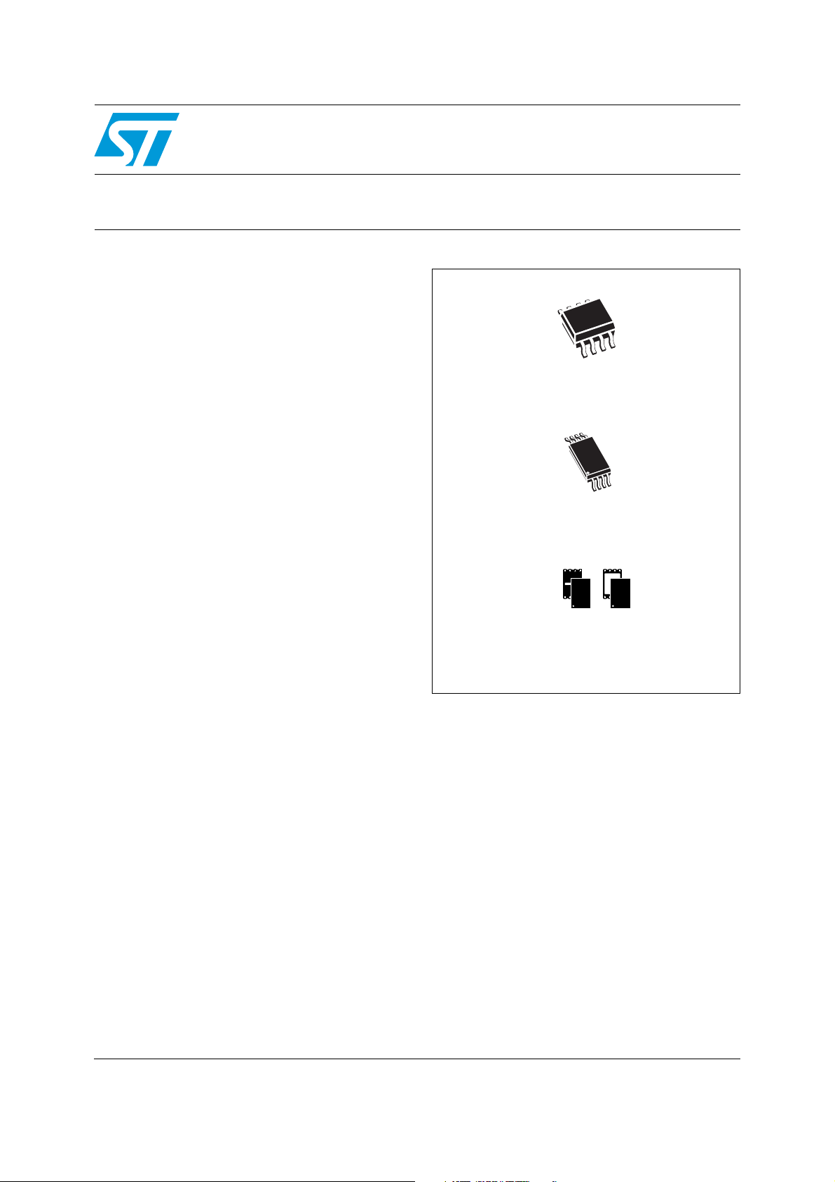
SO8 (MN)
150 mil width
TSSOP8 (DW)
169 mil width
UFDFPN8 (MB, MC)
2 × 3 mm (MLP)
32-Kbit serial SPI bus EEPROM with high-speed clock
Features
■ Compatible with the Serial Peripheral Interface
(SPI) bus
■ Memory array
– 32 Kb (4 Kbytes) of EEPROM
– Page size: 32 bytes
■ Write
– Byte Write within 5 ms
– Page Write within 5 ms
■ Additional Write lockable page (Identification
page)
■ Write Protect: quarter, half or whole memory
array
■ High-speed clock: 20 MHz
■ Single supply voltage:
– 2.5 V to 5.5 V for M95320-W
– 1.8 V to 5.5 V for M95320-R and M95320-
DR
■ Operating temperature range: from -40°C up to
+85°C
■ Enhanced ESD protection
■ More than 4 million Write cycles
■ More than 200-year data retention
■ Packages
– RoHS compliant and halogen-free
(ECOPACK
®
)
Datasheet − production data
May 2012 Doc ID 5711 Rev 14 1/48
This is information on a product in full production.
www.st.com
1

Contents M95320-W M95320-R M95320-DR
Contents
1 Description . . . . . . . . . . . . . . . . . . . . . . . . . . . . . . . . . . . . . . . . . . . . . . . . . 6
2 Memory organization . . . . . . . . . . . . . . . . . . . . . . . . . . . . . . . . . . . . . . . . 8
3 Signal description . . . . . . . . . . . . . . . . . . . . . . . . . . . . . . . . . . . . . . . . . . . 9
3.1 Serial Data Output (Q) . . . . . . . . . . . . . . . . . . . . . . . . . . . . . . . . . . . . . . . . 9
3.2 Serial Data Input (D) . . . . . . . . . . . . . . . . . . . . . . . . . . . . . . . . . . . . . . . . . 9
3.3 Serial Clock (C) . . . . . . . . . . . . . . . . . . . . . . . . . . . . . . . . . . . . . . . . . . . . . 9
3.4 Chip Select (S
3.5 Hold (HOLD
3.6 Write Protect (W
3.7 V
3.8 V
supply voltage . . . . . . . . . . . . . . . . . . . . . . . . . . . . . . . . . . . . . . . . . . 10
CC
ground . . . . . . . . . . . . . . . . . . . . . . . . . . . . . . . . . . . . . . . . . . . . . . . . 10
SS
) . . . . . . . . . . . . . . . . . . . . . . . . . . . . . . . . . . . . . . . . . . . . . . 9
) . . . . . . . . . . . . . . . . . . . . . . . . . . . . . . . . . . . . . . . . . . . . . . . . 9
) . . . . . . . . . . . . . . . . . . . . . . . . . . . . . . . . . . . . . . . . . . . 10
4 Connecting to the SPI bus . . . . . . . . . . . . . . . . . . . . . . . . . . . . . . . . . . . 11
4.1 SPI modes . . . . . . . . . . . . . . . . . . . . . . . . . . . . . . . . . . . . . . . . . . . . . . . . 12
5 Operating features . . . . . . . . . . . . . . . . . . . . . . . . . . . . . . . . . . . . . . . . . 13
5.1 Supply voltage (VCC) . . . . . . . . . . . . . . . . . . . . . . . . . . . . . . . . . . . . . . . . 13
5.1.1 Operating supply voltage V
5.1.2 Device reset . . . . . . . . . . . . . . . . . . . . . . . . . . . . . . . . . . . . . . . . . . . . . . 13
5.1.3 Power-up conditions . . . . . . . . . . . . . . . . . . . . . . . . . . . . . . . . . . . . . . . 13
5.1.4 Power-down . . . . . . . . . . . . . . . . . . . . . . . . . . . . . . . . . . . . . . . . . . . . . . 14
5.2 Active Power and Standby Power modes . . . . . . . . . . . . . . . . . . . . . . . . . 14
5.3 Hold condition . . . . . . . . . . . . . . . . . . . . . . . . . . . . . . . . . . . . . . . . . . . . . . 14
CC . . . . . . . . . . . . . . . . . . . . . . . . . . . . . . . . . . . . . . . . . 13
5.4 Status Register . . . . . . . . . . . . . . . . . . . . . . . . . . . . . . . . . . . . . . . . . . . . . 15
5.5 Data protection and protocol control . . . . . . . . . . . . . . . . . . . . . . . . . . . . 15
6 Instructions . . . . . . . . . . . . . . . . . . . . . . . . . . . . . . . . . . . . . . . . . . . . . . . 16
6.1 Write Enable (WREN) . . . . . . . . . . . . . . . . . . . . . . . . . . . . . . . . . . . . . . . 17
6.2 Write Disable (WRDI) . . . . . . . . . . . . . . . . . . . . . . . . . . . . . . . . . . . . . . . . 18
6.3 Read Status Register (RDSR) . . . . . . . . . . . . . . . . . . . . . . . . . . . . . . . . . 19
6.3.1 WIP bit . . . . . . . . . . . . . . . . . . . . . . . . . . . . . . . . . . . . . . . . . . . . . . . . . . 19
2/48 Doc ID 5711 Rev 14

M95320-W M95320-R M95320-DR Contents
6.3.2 WEL bit . . . . . . . . . . . . . . . . . . . . . . . . . . . . . . . . . . . . . . . . . . . . . . . . . 19
6.3.3 BP1, BP0 bits . . . . . . . . . . . . . . . . . . . . . . . . . . . . . . . . . . . . . . . . . . . . . 19
6.3.4 SRWD bit . . . . . . . . . . . . . . . . . . . . . . . . . . . . . . . . . . . . . . . . . . . . . . . . 20
6.4 Write Status Register (WRSR) . . . . . . . . . . . . . . . . . . . . . . . . . . . . . . . . . 20
6.5 Read from Memory Array (READ) . . . . . . . . . . . . . . . . . . . . . . . . . . . . . . 22
6.6 Write to Memory Array (WRITE) . . . . . . . . . . . . . . . . . . . . . . . . . . . . . . . 23
6.6.1 Cycling with Error Correction Code (ECC) . . . . . . . . . . . . . . . . . . . . . . 25
6.7 Read Identification Page (available only in M95320-DR devices) . . . . . . 26
6.8 Write Identification Page (available only in M95320-DR devices) . . . . . . 27
6.9 Read Lock Status (available only in M95320-DR devices) . . . . . . . . . . . . 28
6.10 Lock ID (available only in M95320-DR devices) . . . . . . . . . . . . . . . . . . . . 29
7 Power-up and delivery state . . . . . . . . . . . . . . . . . . . . . . . . . . . . . . . . . . 30
7.1 Power-up state . . . . . . . . . . . . . . . . . . . . . . . . . . . . . . . . . . . . . . . . . . . . . 30
7.2 Initial delivery state . . . . . . . . . . . . . . . . . . . . . . . . . . . . . . . . . . . . . . . . . . 30
8 Maximum rating . . . . . . . . . . . . . . . . . . . . . . . . . . . . . . . . . . . . . . . . . . . . 31
9 DC and AC parameters . . . . . . . . . . . . . . . . . . . . . . . . . . . . . . . . . . . . . . 32
10 Package mechanical data . . . . . . . . . . . . . . . . . . . . . . . . . . . . . . . . . . . . 40
11 Part numbering . . . . . . . . . . . . . . . . . . . . . . . . . . . . . . . . . . . . . . . . . . . . 43
12 Revision history . . . . . . . . . . . . . . . . . . . . . . . . . . . . . . . . . . . . . . . . . . . 44
Doc ID 5711 Rev 14 3/48

List of tables M95320-W M95320-R M95320-DR
List of tables
Table 1. Signal names . . . . . . . . . . . . . . . . . . . . . . . . . . . . . . . . . . . . . . . . . . . . . . . . . . . . . . . . . . . . 6
Table 2. Write-protected block size . . . . . . . . . . . . . . . . . . . . . . . . . . . . . . . . . . . . . . . . . . . . . . . . . 15
Table 3. Instruction set . . . . . . . . . . . . . . . . . . . . . . . . . . . . . . . . . . . . . . . . . . . . . . . . . . . . . . . . . . . 16
Table 4. M95320-DR instruction set . . . . . . . . . . . . . . . . . . . . . . . . . . . . . . . . . . . . . . . . . . . . . . . . . 16
Table 5. Address range bits . . . . . . . . . . . . . . . . . . . . . . . . . . . . . . . . . . . . . . . . . . . . . . . . . . . . . . . 16
Table 6. Status Register format . . . . . . . . . . . . . . . . . . . . . . . . . . . . . . . . . . . . . . . . . . . . . . . . . . . . 20
Table 7. Protection modes . . . . . . . . . . . . . . . . . . . . . . . . . . . . . . . . . . . . . . . . . . . . . . . . . . . . . . . . 21
Table 8. Absolute maximum ratings . . . . . . . . . . . . . . . . . . . . . . . . . . . . . . . . . . . . . . . . . . . . . . . . . 31
Table 9. Operating conditions (M95320-W, device grade 6) . . . . . . . . . . . . . . . . . . . . . . . . . . . . . . 32
Table 10. Operating conditions (M95320-R and M95320-DR, device grade 6) . . . . . . . . . . . . . . . . . 32
Table 11. AC measurement conditions. . . . . . . . . . . . . . . . . . . . . . . . . . . . . . . . . . . . . . . . . . . . . . . . 32
Table 12. Capacitance . . . . . . . . . . . . . . . . . . . . . . . . . . . . . . . . . . . . . . . . . . . . . . . . . . . . . . . . . . . . 33
Table 13. Cycling performance by groups of four bytes . . . . . . . . . . . . . . . . . . . . . . . . . . . . . . . . . . . 33
Table 14. Memory cell data retention . . . . . . . . . . . . . . . . . . . . . . . . . . . . . . . . . . . . . . . . . . . . . . . . . 33
Table 15. DC characteristics (M95320-W, device grade 6) . . . . . . . . . . . . . . . . . . . . . . . . . . . . . . . . 34
Table 16. DC characteristics (M95320-R, M95320-DR, device grade 6) . . . . . . . . . . . . . . . . . . . . . . 35
Table 17. AC characteristics (M95320-W, device grade 6) . . . . . . . . . . . . . . . . . . . . . . . . . . . . . . . . 36
Table 18. AC characteristics (M95320-R, M95320-DR, device grade 6) . . . . . . . . . . . . . . . . . . . . . . 37
Table 19. SO8N – 8-lead plastic small outline, 150 mils body width, mechanical data . . . . . . . . . . . 40
Table 20. UFDFPN8 (MLP8) 8-lead ultra thin fine pitch dual flat package no lead
2 x 3 mm, data . . . . . . . . . . . . . . . . . . . . . . . . . . . . . . . . . . . . . . . . . . . . . . . . . . . . . . . . . . 41
Table 21. TSSOP8 – 8-lead thin shrink small outline, package mechanical data. . . . . . . . . . . . . . . . 42
Table 22. Ordering information scheme . . . . . . . . . . . . . . . . . . . . . . . . . . . . . . . . . . . . . . . . . . . . . . . 43
Table 23. Document revision history . . . . . . . . . . . . . . . . . . . . . . . . . . . . . . . . . . . . . . . . . . . . . . . . . 44
4/48 Doc ID 5711 Rev 14

M95320-W M95320-R M95320-DR List of figures
List of figures
Figure 1. Logic diagram . . . . . . . . . . . . . . . . . . . . . . . . . . . . . . . . . . . . . . . . . . . . . . . . . . . . . . . . . . . . 6
Figure 2. 8-pin package connections (top view) . . . . . . . . . . . . . . . . . . . . . . . . . . . . . . . . . . . . . . . . . 7
Figure 3. Block diagram . . . . . . . . . . . . . . . . . . . . . . . . . . . . . . . . . . . . . . . . . . . . . . . . . . . . . . . . . . . . 8
Figure 4. Bus master and memory devices on the SPI bus . . . . . . . . . . . . . . . . . . . . . . . . . . . . . . . . 11
Figure 5. SPI modes supported . . . . . . . . . . . . . . . . . . . . . . . . . . . . . . . . . . . . . . . . . . . . . . . . . . . . . 12
Figure 6. Hold condition activation . . . . . . . . . . . . . . . . . . . . . . . . . . . . . . . . . . . . . . . . . . . . . . . . . . . 14
Figure 7. Write Enable (WREN) sequence . . . . . . . . . . . . . . . . . . . . . . . . . . . . . . . . . . . . . . . . . . . . 17
Figure 8. Write Disable (WRDI) sequence . . . . . . . . . . . . . . . . . . . . . . . . . . . . . . . . . . . . . . . . . . . . . 18
Figure 9. Read Status Register (RDSR) sequence . . . . . . . . . . . . . . . . . . . . . . . . . . . . . . . . . . . . . . 19
Figure 10. Write Status Register (WRSR) sequence . . . . . . . . . . . . . . . . . . . . . . . . . . . . . . . . . . . . . . 20
Figure 11. Read from Memory Array (READ) sequence . . . . . . . . . . . . . . . . . . . . . . . . . . . . . . . . . . . 22
Figure 12. Byte Write (WRITE) sequence . . . . . . . . . . . . . . . . . . . . . . . . . . . . . . . . . . . . . . . . . . . . . . 23
Figure 13. Page Write (WRITE) sequence . . . . . . . . . . . . . . . . . . . . . . . . . . . . . . . . . . . . . . . . . . . . . 24
Figure 14. Read Identification Page sequence . . . . . . . . . . . . . . . . . . . . . . . . . . . . . . . . . . . . . . . . . . 26
Figure 15. Write Identification Page sequence . . . . . . . . . . . . . . . . . . . . . . . . . . . . . . . . . . . . . . . . . . 27
Figure 16. Read Lock Status sequence . . . . . . . . . . . . . . . . . . . . . . . . . . . . . . . . . . . . . . . . . . . . . . . . 28
Figure 17. Lock ID sequence . . . . . . . . . . . . . . . . . . . . . . . . . . . . . . . . . . . . . . . . . . . . . . . . . . . . . . . . 29
Figure 18. AC measurement I/O waveform . . . . . . . . . . . . . . . . . . . . . . . . . . . . . . . . . . . . . . . . . . . . . 32
Figure 19. Serial input timing . . . . . . . . . . . . . . . . . . . . . . . . . . . . . . . . . . . . . . . . . . . . . . . . . . . . . . . . 38
Figure 20. Hold timing . . . . . . . . . . . . . . . . . . . . . . . . . . . . . . . . . . . . . . . . . . . . . . . . . . . . . . . . . . . . . 38
Figure 21. Serial output timing . . . . . . . . . . . . . . . . . . . . . . . . . . . . . . . . . . . . . . . . . . . . . . . . . . . . . . . 39
Figure 22. SO8N – 8-lead plastic small outline, 150 mils body width, package outline . . . . . . . . . . . . 40
Figure 23. UFDFPN8 (MLP8) - 8-lead ultra thin fine pitch dual flat no lead, package
outline . . . . . . . . . . . . . . . . . . . . . . . . . . . . . . . . . . . . . . . . . . . . . . . . . . . . . . . . . . . . . . . . . 41
Figure 24. TSSOP8 – 8-lead thin shrink small outline, package outline . . . . . . . . . . . . . . . . . . . . . . . 42
Doc ID 5711 Rev 14 5/48
Description M95320-W M95320-R M95320-DR
AI01789C
S
V
CC
M95xxx
HOLD
V
SS
W
Q
C
D
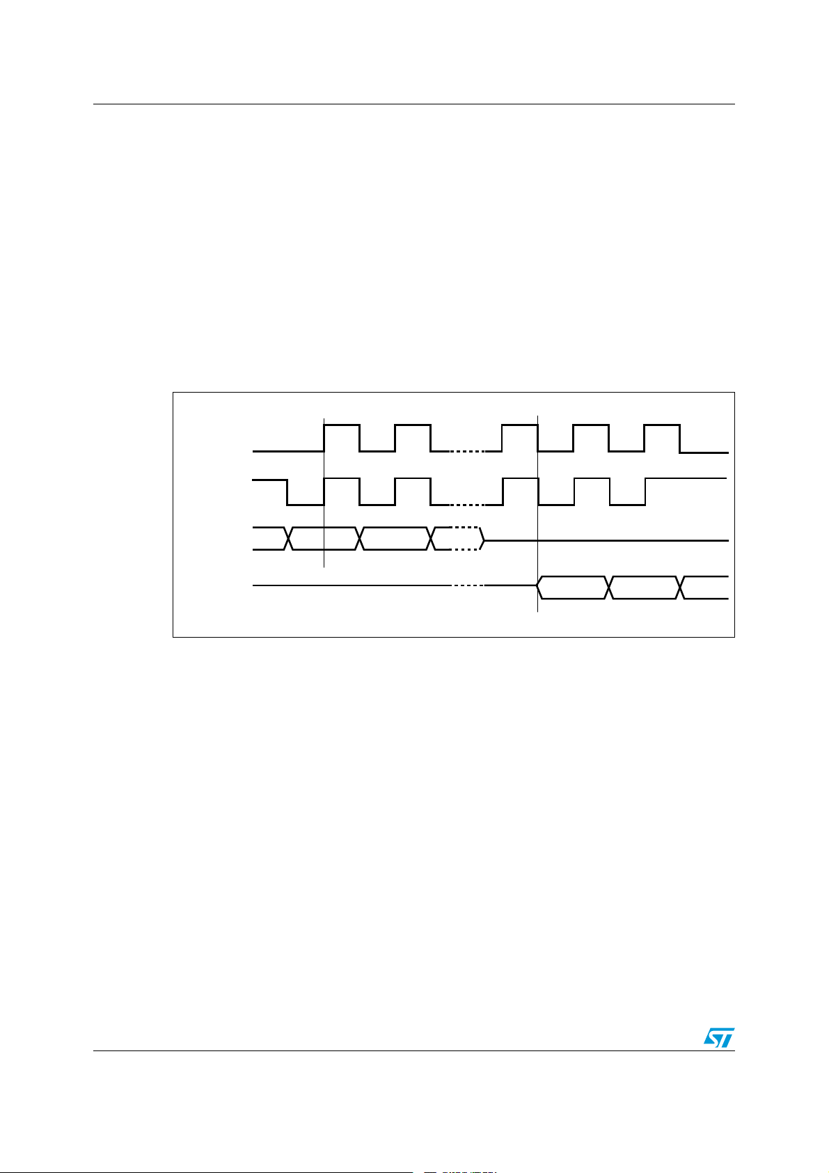
1 Description
The M95320 devices are Electrically Erasable PROgrammable Memories (EEPROMs)
organized as 4096 x 8 bits, accessed through the SPI bus.
The M95320 devices can operate with a supply range from 1.8 V up to 5.5 V, and are
guaranteed over the -40 °C/+85 °C temperature range.
The M95320-D offers an additional page, named the Identification Page (32 bytes). The
Identification Page can be used to store sensitive application parameters which can be
(later) permanently locked in Read-only mode.
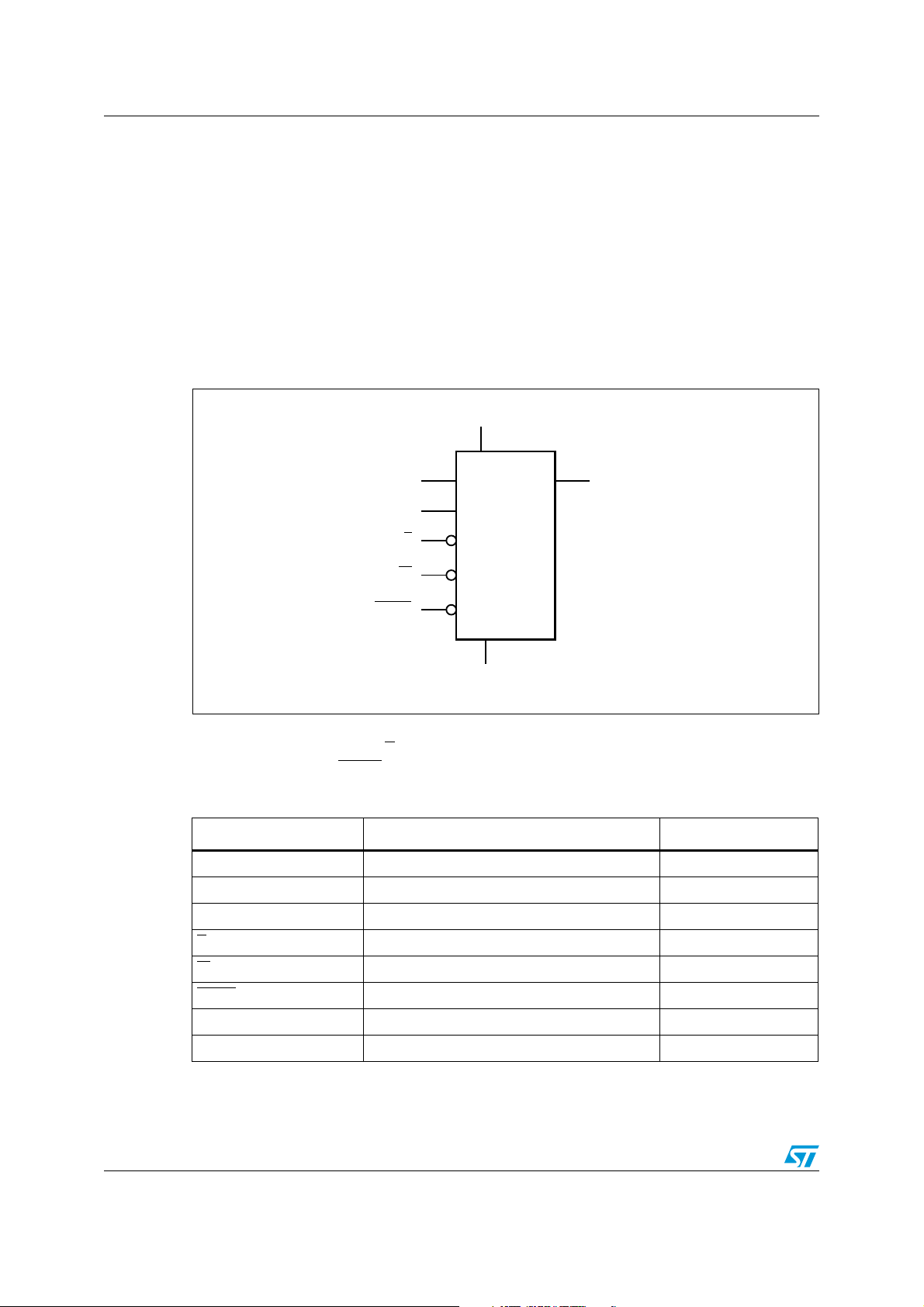
Figure 1. Logic diagram
The SPI bus signals are C, D and Q, as shown in Figure 1 and Tab l e 1 . The device is
selected when Chip Select (S
interrupted when the HOLD
Table 1. Signal names
Signal name Function Direction
C Serial Clock Input
D Serial Data Input Input
Q Serial Data Output Output
S
W
Hold Input
HOLD
6/48 Doc ID 5711 Rev 14
V
CC
V
SS
) is driven low. Communications with the device can be
is driven low.
Chip Select Input
Write Protect Input
Supply voltage
Ground

M95320-W M95320-R M95320-DR Description
DV
SS
C
HOLDQ
SV
CC
W
AI01790D
M95xxx
1
2
3
4
8
7
6
5
Figure 2. 8-pin package connections (top view)
1. See Section 10: Package mechanical data section for package dimensions, and how to identify pin 1.
Doc ID 5711 Rev 14 7/48
Memory organization M95320-W M95320-R M95320-DR
-36
(/,$
3
7
#ONTROLLOGIC
(IGHVOLTAGE
GENERATOR
)/SHIFTREGISTER
!DDRESSREGISTER
ANDCOUNTER
$ATA
REGISTER
PAGE
8DECODER
9DECODER
#
$
1
3IZEOFTHE
2EADONLY
%%02/AREA
3TATUS
REGISTER
)DENTIFICATIONPAGE
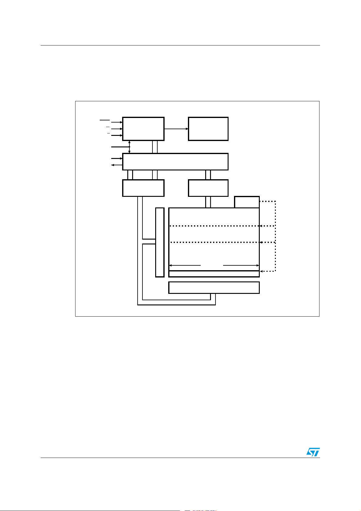
2 Memory organization
The memory is organized as shown in the following figure.
Figure 3. Block diagram
8/48 Doc ID 5711 Rev 14

M95320-W M95320-R M95320-DR Signal description
3 Signal description
During all operations, VCC must be held stable and within the specified valid range:
V
(min) to VCC(max).
CC
All of the input and output signals must be held high or low (according to voltages of V
V
, VIL or VOL, as specified in Section 9: DC and AC parameters). These signals are
OH
described next.
3.1 Serial Data Output (Q)
This output signal is used to transfer data serially out of the device. Data is shifted out on the
falling edge of Serial Clock (C).
3.2 Serial Data Input (D)
This input signal is used to transfer data serially into the device. It receives instructions,
addresses, and the data to be written. Values are latched on the rising edge of Serial Clock
(C).
,
IH
3.3 Serial Clock (C)
This input signal provides the timing of the serial interface. Instructions, addresses, or data
present at Serial Data Input (D) are latched on the rising edge of Serial Clock (C). Data on
Serial Data Output (Q) change from the falling edge of Serial Clock (C).
3.4 Chip Select (S)
When this input signal is high, the device is deselected and Serial Data Output (Q) is at high
impedance. The device is in the Standby Power mode, unless an internal Write cycle is in
progress. Driving Chip Select (S
After power-up, a falling edge on Chip Select (S
instruction.
3.5 Hold (HOLD)
The Hold (HOLD) signal is used to pause any serial communications with the device without
deselecting the device.
During the Hold condition, the Serial Data Output (Q) is high impedance, and Serial Data
Input (D) and Serial Clock (C) are Don’t Care.
To start the Hold condition, the device must be selected, with Chip Select (S
) low selects the device, placing it in the Active Power mode.
) is required prior to the start of any
) driven low.
Doc ID 5711 Rev 14 9/48

Signal description M95320-W M95320-R M95320-DR
3.6 Write Protect (W)
The main purpose of this input signal is to freeze the size of the area of memory that is
protected against Write instructions (as specified by the values in the BP1 and BP0 bits of
the Status Register).
This pin must be driven either high or low, and must be stable during all Write instructions.
3.7 V
supply voltage
CC
VCC is the supply voltage.
3.8 VSS ground
VSS is the reference for all signals, including the VCC supply voltage.
10/48 Doc ID 5711 Rev 14
M95320-W M95320-R M95320-DR Connecting to the SPI bus
AI12836b
SPI Bus Master
SPI Memory
Device
SDO
SDI
SCK
CQD
S
SPI Memory
Device
CQD
S
SPI Memory
Device
CQD
S
CS3 CS2 CS1
SPI Interface with
(CPOL, CPHA) =
(0, 0) or (1, 1)
W
HOLD
W
HOLD
W
HOLD
RR R
V
CC
V
CC
V
CC
V
CC
V
SS
V
SS
V
SS
V
SS
R
4 Connecting to the SPI bus
All instructions, addresses and input data bytes are shifted in to the device, most significant
bit first. The Serial Data Input (D) is sampled on the first rising edge of the Serial Clock (C)
after Chip Select (S
All output data bytes are shifted out of the device, most significant bit first. The Serial Data
Output (Q) is latched on the first falling edge of the Serial Clock (C) after the instruction
(such as the Read from Memory Array and Read Status Register instructions) have been
clocked into the device.
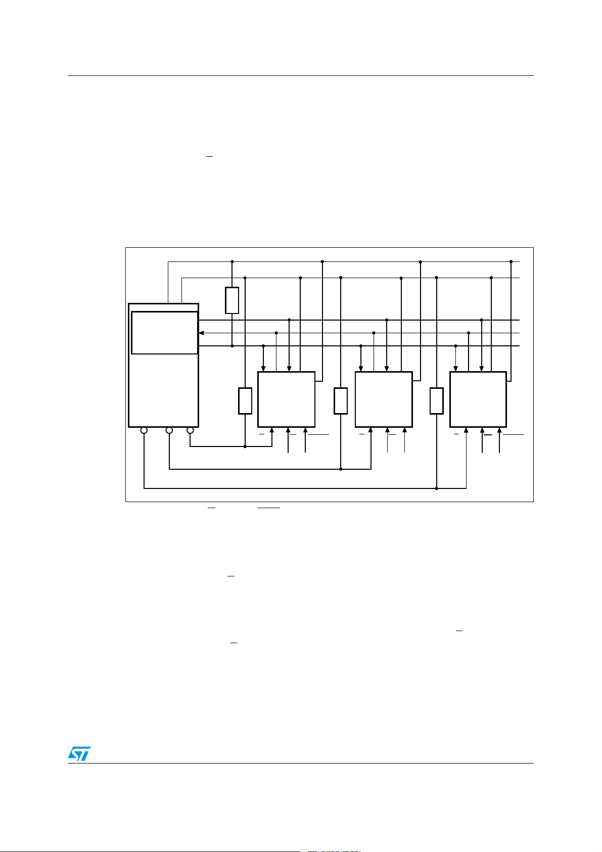
Figure 4. Bus master and memory devices on the SPI bus
) goes low.
1. The Write Protect (W) and Hold (HOLD) signals should be driven, high or low as appropriate.
Figure 4 shows an example of three memory devices connected to an SPI bus master. Only
one memory device is selected at a time, so only one memory device drives the Serial Data
Output (Q) line at a time. The other memory devices are high impedance.
The pull-up resistor R (represented in Figure 4) ensures that a device is not selected if the
Bus Master leaves the S
line in the high impedance state.
In applications where the Bus Master may leave all SPI bus lines in high impedance at the
same time (for example, if the Bus Master is reset during the transmission of an instruction),
the clock line (C) must be connected to an external pull-down resistor so that, if all
inputs/outputs become high impedance, the C line is pulled low (while the S
high): this ensures that S
t
requirement is met. The typical value of R is 100 kΩ..
SHCH
and C do not become high at the same time, and so, that the
Doc ID 5711 Rev 14 11/48
line is pulled
Connecting to the SPI bus M95320-W M95320-R M95320-DR
AI01438B
C
MSB
CPHA
D
0
1
CPOL
0
1
Q
C
MSB
4.1 SPI modes
These devices can be driven by a microcontroller with its SPI peripheral running in either of
the following two modes:
● CPOL=0, CPHA=0
● CPOL=1, CPHA=1
For these two modes, input data is latched in on the rising edge of Serial Clock (C), and
output data is available from the falling edge of Serial Clock (C).
The difference between the two modes, as shown in Figure 5, is the clock polarity when the
bus master is in Stand-by mode and not transferring data:
● C remains at 0 for (CPOL=0, CPHA=0)
● C remains at 1 for (CPOL=1, CPHA=1)
Figure 5. SPI modes supported
12/48 Doc ID 5711 Rev 14

M95320-W M95320-R M95320-DR Operating features
5 Operating features
5.1 Supply voltage (VCC)
5.1.1 Operating supply voltage V
Prior to selecting the memory and issuing instructions to it, a valid and stable VCC voltage
within the specified [V
(min), VCC(max)] range must be applied (see Operating conditions
CC
in Section 9: DC and AC parameters). This voltage must remain stable and valid until the
end of the transmission of the instruction and, for a Write instruction, until the completion of
the internal write cycle (t
recommended to decouple the V
10 nF to 100 nF) close to the V
). In order to secure a stable DC supply voltage, it is
W
CC
CC/VSS
5.1.2 Device reset
In order to prevent erroneous instruction decoding and inadvertent Write operations during
power-up, a power-on-reset (POR) circuit is included. At power-up, the device does not
respond to any instruction until VCC reaches the POR threshold voltage. This threshold is
lower than the minimum V
and AC parameters).
At power-up, when V
CC
following state:
● in Standby Power mode,
● deselected,
● Status Register values:
– The Write Enable Latch (WEL) bit is reset to 0.
– The Write In Progress (WIP) bit is reset to 0.
– The SRWD, BP1 and BP0 bits remain unchanged (non-volatile bits).
operating voltage (see Operating conditions in Section 9: DC
CC
passes over the POR threshold, the device is reset and is in the
CC
line with a suitable capacitor (usually of the order of
device pins.
It is important to note that the device must not be accessed until V
stable level within the specified [V
conditions in Section 9: DC and AC parameters.
5.1.3 Power-up conditions
When the power supply is turned on, VCC rises continuously from VSS to VCC. During this
time, the Chip Select (S
therefore recommended to connect the S
Figure 4).
In addition, the Chip Select (S
sensitive as well as level-sensitive: after power-up, the device does not become selected
until a falling edge has first been detected on Chip Select (S
(S
) must have been high, prior to going low to start the first operation.
The V
voltage has to rise continuously from 0 V up to the minimum VCC operating voltage
CC
defined under Operating conditions in Section 9: DC and AC parameters, and the rise time
must not vary faster than 1 V/µs.
) line is not allowed to float but should follow the VCC voltage. It is
reaches a valid and
(min), VCC(max)] range, as defined under Operating
CC
CC
line to VCC via a suitable pull-up resistor (see
) input offers a built-in safety feature, as the S input is edge-
). This ensures that Chip Select
Doc ID 5711 Rev 14 13/48
Operating features M95320-W M95320-R M95320-DR
AI02029D
HOLD
C
Hold
Condition
Hold
Condition
5.1.4 Power-down
During power-down (continuous decrease of the VCC supply voltage below the minimum
V
operating voltage defined under Operating conditions in Section 9: DC and AC
CC
parameters), the device must be:
● deselected (Chip Select S should be allowed to follow the voltage applied on V
● in Standby Power mode (there should not be any internal write cycle in progress).
CC
),
5.2 Active Power and Standby Power modes
When Chip Select (S) is low, the device is selected, and in the Active Power mode. The
device consumes I
When Chip Select (S
.
CC
) is high, the device is deselected. If a Write cycle is not currently in
progress, the device then goes into the Standby Power mode, and the device consumption
drops to I
, as specified in DC characteristics (see Section 9: DC and AC parameters).
CC1
5.3 Hold condition
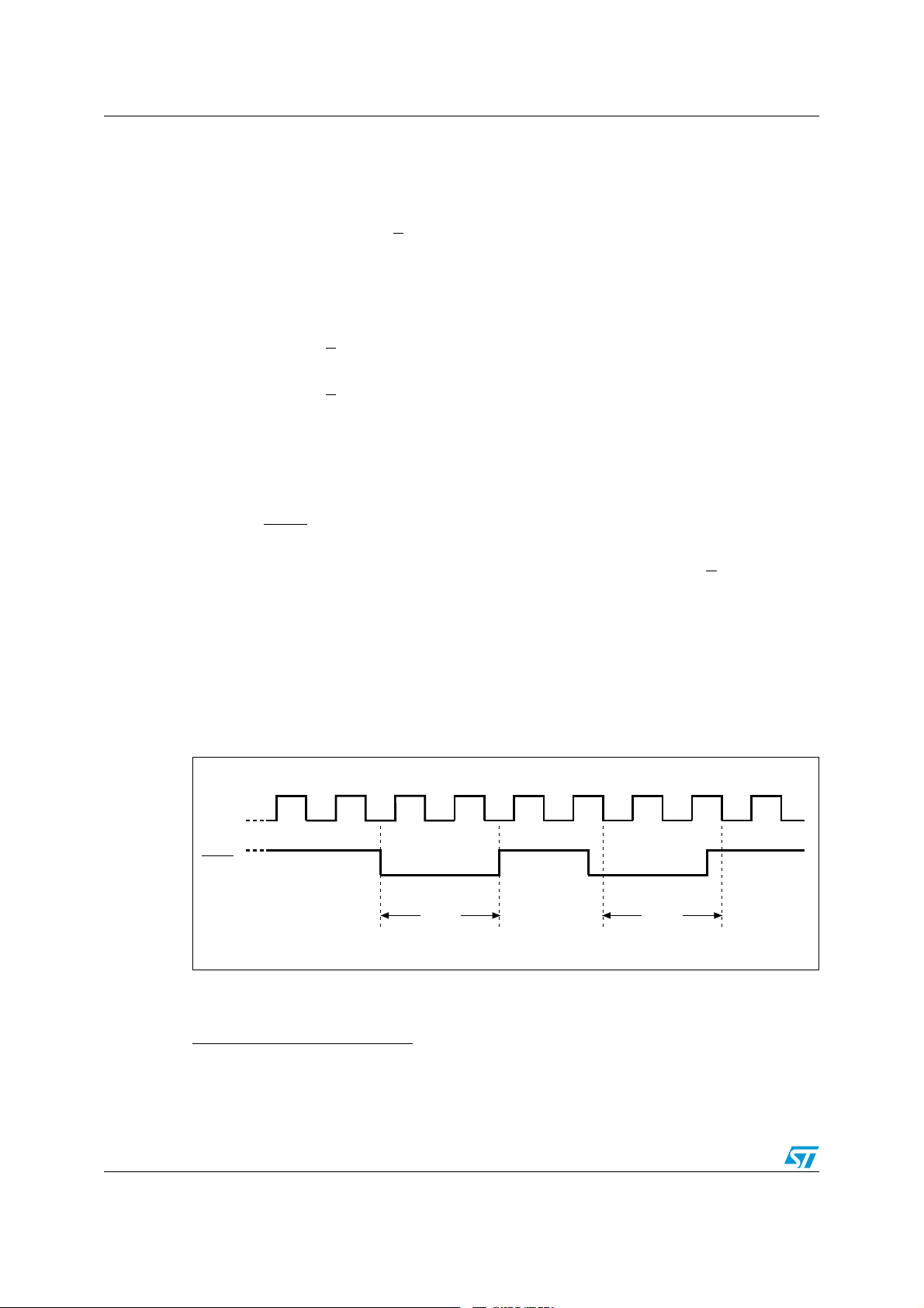
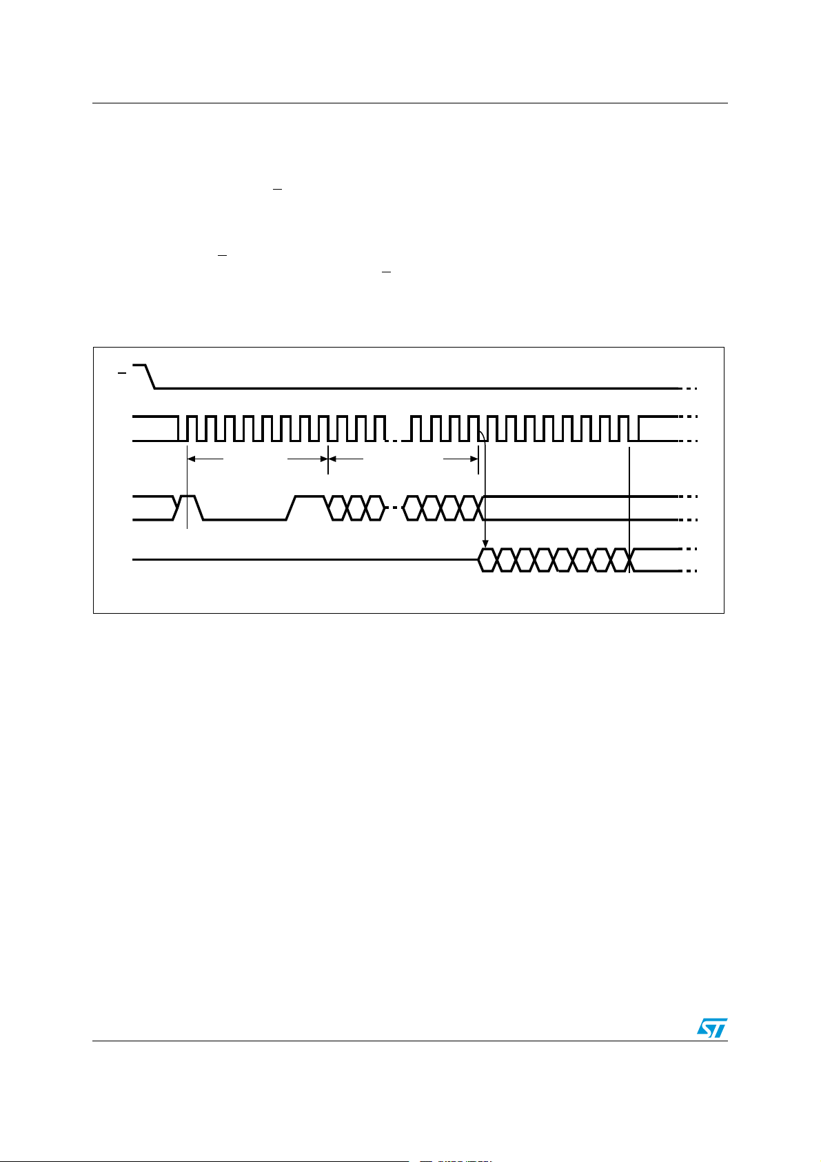
The Hold (HOLD) signal is used to pause any serial communications with the device without
resetting the clocking sequence.
To enter the Hold condition, the device must be selected, with Chip Select (S
) low.
During the Hold condition, the Serial Data Output (Q) is high impedance, and the Serial
Data Input (D) and the Serial Clock (C) are Don’t Care.
Normally, the device is kept selected for the whole duration of the Hold condition.
Deselecting the device while it is in the Hold condition has the effect of resetting the state of
the device, and this mechanism can be used if required to reset any processes that had
been in progress.
(a)(b)
Figure 6. Hold condition activation
The Hold condition starts when the Hold (HOLD) signal is driven low when Serial Clock (C)
is already low (as shown in Figure 6).
a. This resets the internal logic, except the WEL and WIP bits of the Status Register.
b. In the specific case where the device has shifted in a Write command (Inst + Address + data bytes, each data
byte being exactly 8 bits), deselecting the device also triggers the Write cycle of this decoded command.
14/48 Doc ID 5711 Rev 14
M95320-W M95320-R M95320-DR Operating features
The Hold condition ends when the Hold (HOLD) signal is driven high when Serial Clock (C)
is already low.
Figure 6 also shows what happens if the rising and falling edges are not timed to coincide
with Serial Clock (C) being low.
5.4 Status Register
The Status Register contains a number of status and control bits that can be read or set (as
appropriate) by specific instructions. See Section 6.3: Read Status Register (RDSR) for a
detailed description of the Status Register bits.
5.5 Data protection and protocol control
The device features the following data protection mechanisms:
● Before accepting the execution of the Write and Write Status Register instructions, the
device checks whether the number of clock pulses comprised in the instructions is a
multiple of eight.
● All instructions that modify data must be preceded by a Write Enable (WREN)
instruction to set the Write Enable Latch (WEL) bit.
● The Block Protect (BP1, BP0) bits in the Status Register are used to configure part of
the memory as read-only.
● The Write Protect (W) signal is used to protect the Block Protect (BP1, BP0) bits in the
Status Register.
For any instruction to be accepted, and executed, Chip Select (S
) must be driven high after
the rising edge of Serial Clock (C) for the last bit of the instruction, and before the next rising
edge of Serial Clock (C).
Two points should be noted in the previous sentence:
● The “last bit of the instruction” can be the eighth bit of the instruction code, or the eighth
bit of a data byte, depending on the instruction (except for Read Status Register
(RDSR) and Read (READ) instructions).
● The “next rising edge of Serial Clock (C)” might (or might not) be the next bus
transaction for some other device on the SPI bus.
Table 2. Write-protected block size
Status Register bits
Protected block Protected array addresses
BP1 BP0
0 0 none none
0 1 Upper quarter 0C00h - 0FFFh
1 0 Upper half 0800h - 0FFFh
1 1 Whole memory 0000h - 0FFFh
Doc ID 5711 Rev 14 15/48

Instructions M95320-W M95320-R M95320-DR
6 Instructions
Each instruction starts with a single-byte code, as summarized in Ta b le 3 .
If an invalid instruction is sent (one not contained in Ta bl e 3 ), the device automatically
deselects itself.
Table 3. Instruction set
Instruction Description Instruction format
WREN Write Enable 0000 0110
WRDI Write Disable 0000 0100
RDSR Read Status Register 0000 0101
WRSR Write Status Register 0000 0001
READ Read from Memory Array 0000 0011
WRITE Write to Memory Array 0000 0010
Table 4. M95320-DR instruction set
Instruction Description
Instruction
format
WREN Write Enable 0000 0110
WRDI Write Disable 0000 0100
RDSR Read Status Register 0000 0101
WRSR Write Status Register 0000 0001
READ Read from Memory Array 0000 0011
WRITE Write to Memory Array 0000 0010
Read Identification
Page
Write Identification
Page
Reads the page dedicated to identification. 1000 0011
Writes the page dedicated to identification. 1000 0010
Read Lock Status Reads the lock status of the Identification Page. 1000 0011
Lock ID Locks the Identification page in read-only mode. 1000 0010
1. Address bit A10 must be 0, all other address bits are Don't Care.
2. Address bit A10 must be 1, all other address bits are Don't Care.
Table 5. Address range bits
Address significant bits A11-A0
1. Upper MSBs are Don’t Care.
(1)
(1)
(1)
(2)
(2)
16/48 Doc ID 5711 Rev 14

M95320-W M95320-R M95320-DR Instructions
C
D
AI02281E
S
Q
21 34567
High Impedance
0
Instruction
6.1 Write Enable (WREN)
The Write Enable Latch (WEL) bit must be set prior to each WRITE and WRSR instruction.
The only way to do this is to send a Write Enable instruction to the device.
As shown in Figure 7, to send this instruction to the device, Chip Select (S
) is driven low,
and the bits of the instruction byte are shifted in, on Serial Data Input (D). The device then
enters a wait state. It waits for the device to be deselected, by Chip Select (S
) being driven
high.
Figure 7. Write Enable (WREN) sequence
Doc ID 5711 Rev 14 17/48

Instructions M95320-W M95320-R M95320-DR
C
D
AI03750D
S
Q
21 34567
High Impedance
0
Instruction
6.2 Write Disable (WRDI)
One way of resetting the Write Enable Latch (WEL) bit is to send a Write Disable instruction
to the device.
As shown in Figure 8, to send this instruction to the device, Chip Select (S
) is driven low,
and the bits of the instruction byte are shifted in, on Serial Data Input (D).
The device then enters a wait state. It waits for a the device to be deselected, by Chip Select
(S
) being driven high.
The Write Enable Latch (WEL) bit, in fact, becomes reset by any of the following events:
● Power-up
● WRDI instruction execution
● WRSR instruction completion
● WRITE instruction completion.
Figure 8. Write Disable (WRDI) sequence
18/48 Doc ID 5711 Rev 14

M95320-W M95320-R M95320-DR Instructions
C
D
S
21 3456789101112131415
Instruction
0
AI02031E
Q
7 6543210
Status Register Out
High Impedance
MSB
7 6543210
Status Register Out
MSB
7
6.3 Read Status Register (RDSR)
The Read Status Register (RDSR) instruction is used to read the Status Register. The
Status Register may be read at any time, even while a Write or Write Status Register cycle
is in progress. When one of these cycles is in progress, it is recommended to check the
Write In Progress (WIP) bit before sending a new instruction to the device. It is also possible
to read the Status Register continuously, as shown in Figure 9.
Figure 9. Read Status Register (RDSR) sequence
The status and control bits of the Status Register are as follows:
6.3.1 WIP bit
The Write In Progress (WIP) bit indicates whether the memory is busy with a Write or Write
Status Register cycle. When set to 1, such a cycle is in progress, when reset to 0, no such
cycle is in progress.
6.3.2 WEL bit
The Write Enable Latch (WEL) bit indicates the status of the internal Write Enable Latch.
When set to 1, the internal Write Enable Latch is set. When set to 0, the internal Write
Enable Latch is reset, and no Write or Write Status Register instruction is accepted.
The WEL bit is returned to its reset state by the following events:
● Power-up
● Write Disable (WRDI) instruction completion
● Write Status Register (WRSR) instruction completion
● Write (WRITE) instruction completion
6.3.3 BP1, BP0 bits
The Block Protect (BP1, BP0) bits are non volatile. They define the size of the area to be
software-protected against Write instructions. These bits are written with the Write Status
Register (WRSR) instruction. When one or both of the Block Protect (BP1, BP0) bits is set
to 1, the relevant memory area (as defined in Ta bl e 2 ) becomes protected against Write
(WRITE) instructions. The Block Protect (BP1, BP0) bits can be written provided that the
Hardware Protected mode has not been set.
Doc ID 5711 Rev 14 19/48

Instructions M95320-W M95320-R M95320-DR
C
D
AI02282D
S
Q
21 3456789101112131415
High Impedance
Instruction Status
Register In
0
765432 0
1
MSB
6.3.4 SRWD bit
The Status Register Write Disable (SRWD) bit is operated in conjunction with the Write
Protect (W
signal enable the device to be put in the Hardware Protected mode (when the Status
Register Write Disable (SRWD) bit is set to 1, and Write Protect (W
mode, the non-volatile bits of the Status Register (SRWD, BP1, BP0) become read-only bits
and the Write Status Register (WRSR) instruction is no longer accepted for execution.
Table 6. Status Register format
Status Register Write Protect
) signal. The Status Register Write Disable (SRWD) bit and Write Protect (W)
) is driven low). In this
b7 b0
SRWD 0 0 0 BP1 BP0 WEL WIP
Block Protect bits
Write Enable Latch bit
Write In Progress bit
6.4 Write Status Register (WRSR)
The Write Status Register (WRSR) instruction is used to write new values to the Status
Register. Before it can be accepted, a Write Enable (WREN) instruction must have been
previously executed.
The Write Status Register (WRSR) instruction is entered by driving Chip Select (S
followed by the instruction code, the data byte on Serial Data input (D) and Chip Select (S
driven high. Chip Select (S
latches in the eighth bit of the data byte, and before the next rising edge of Serial Clock (C).
Otherwise, the Write Status Register (WRSR) instruction is not executed.
The instruction sequence is shown in Figure 10.
Figure 10. Write Status Register (WRSR) sequence
) must be driven high after the rising edge of Serial Clock (C) that
) low,
)
20/48 Doc ID 5711 Rev 14

M95320-W M95320-R M95320-DR Instructions
Driving the Chip Select (S) signal high at a byte boundary of the input data triggers the selftimed Write cycle that takes t
to complete (as specified in AC tables under Section 9: DC
W
and AC parameters).
While the Write Status Register cycle is in progress, the Status Register may still be read to
check the value of the Write in progress (WIP) bit: the WIP bit is 1 during the self-timed
Write cycle t
also reset at the end of the Write cycle t
, and 0 when the Write cycle is complete. The WEL bit (Write Enable Latch) is
W
.
W
The Write Status Register (WRSR) instruction enables the user to change the values of the
BP1, BP0 and SRWD bits:
● The Block Protect (BP1, BP0) bits define the size of the area that is to be treated as
read-only, as defined in Ta bl e 2 .
● The SRWD (Status Register Write Disable) bit, in accordance with the signal read on
the Write Protect pin (W
), enables the user to set or reset the Write protection mode of
the Status Register itself, as defined in Tab l e 7 . When in Write-protected mode, the
Write Status Register (WRSR) instruction is not executed.
The contents of the SRWD and BP1, BP0 bits are updated after the completion of the
WRSR instruction, including the t
Write cycle.
W
The Write Status Register (WRSR) instruction has no effect on the b6, b5, b4, b1, b0 bits in
the Status Register. Bits b6, b5, b4 are always read as 0.
Table 7. Protection modes
W
SRWD
signal
10
00
11
01
1. As defined by the values in the Block Protect (BP1, BP0) bits of the Status Register. See Table 2.
bit
Mode
Softwareprotected
(SPM)
Hardware-
protected
(HPM)
Write protection of the
Status Register
Status Register is
writable (if the WREN
instruction has set the
WEL bit).
The values in the BP1
and BP0 bits can be
changed.
Status Register is
Hardware writeprotected.
The values in the BP1
and BP0 bits cannot be
changed.
Protected area
Write-protected
Write-protected
Memory content
(1)
Unprotected area
Ready to accept
Write instructions
Ready to accept
Write instructions
The protection features of the device are summarized in Tab l e 7 .
When the Status Register Write Disable (SRWD) bit in the Status Register is 0 (its initial
delivery state), it is possible to write to the Status Register (provided that the WEL bit has
previously been set by a WREN instruction), regardless of the logic level applied on the
Write Protect (W
) input pin.
(1)
Doc ID 5711 Rev 14 21/48

Instructions M95320-W M95320-R M95320-DR
C
D
AI01793D
S
Q
15
21 345678910 2021222324252627
1413 3210
28 29 30
76543 1 7
0
High Impedance
Data Out 1
Instruction 16-Bit Address
0
MSB
MSB
2
31
Data Out 2
When the Status Register Write Disable (SRWD) bit in the Status Register is set to 1, two
cases should be considered, depending on the state of the Write Protect (W
● If Write Protect (W) is driven high, it is possible to write to the Status Register (provided
) input pin:
that the WEL bit has previously been set by a WREN instruction).
● If Write Protect (W) is driven low, it is not possible to write to the Status Register even if
the WEL bit has previously been set by a WREN instruction. (Attempts to write to the
Status Register are rejected, and are not accepted for execution). As a consequence,
all the data bytes in the memory area, which are Software-protected (SPM) by the
Block Protect (BP1, BP0) bits in the Status Register, are also hardware-protected
against data modification.
Regardless of the order of the two events, the Hardware-protected mode (HPM) can be
entered by:
● either setting the SRWD bit after driving the Write Protect (W) input pin low,
● or driving the Write Protect (W) input pin low after setting the SRWD bit.
Once the Hardware-protected mode (HPM) has been entered, the only way of exiting it is to
pull high the Write Protect (W
) input pin.
If the Write Protect (W
) input pin is permanently tied high, the Hardware-protected mode
(HPM) can never be activated, and only the Software-protected mode (SPM), using the
Block Protect (BP1, BP0) bits in the Status Register, can be used.
6.5 Read from Memory Array (READ)
As shown in Figure 11, to send this instruction to the device, Chip Select (S) is first driven
low. The bits of the instruction byte and address bytes are then shifted in, on Serial Data
Input (D). The address is loaded into an internal address register, and the byte of data at
that address is shifted out, on Serial Data Output (Q).
Figure 11. Read from Memory Array (READ) sequence
1. Depending on the memory size, as shown in Table 5, the most significant address bits are Don’t Care.
If Chip Select (S) continues to be driven low, the internal address register is incremented
automatically, and the byte of data at the new address is shifted out.
22/48 Doc ID 5711 Rev 14
M95320-W M95320-R M95320-DR Instructions
C
D
AI01795D
S
Q
15
21 345678910 2021222324252627
1413 3210
28 29 30
High Impedance
Instruction 16-Bit Address
0
765432 0
1
Data Byte
31
When the highest address is reached, the address counter rolls over to zero, allowing the
Read cycle to be continued indefinitely. The whole memory can, therefore, be read with a
single READ instruction.
The Read cycle is terminated by driving Chip Select (S
Select (S
) signal can occur at any time during the cycle.
The instruction is not accepted, and is not executed, if a Write cycle is currently in progress.
6.6 Write to Memory Array (WRITE)
As shown in Figure 12, to send this instruction to the device, Chip Select (S) is first driven
low. The bits of the instruction byte, address byte, and at least one data byte are then shifted
in, on Serial Data Input (D).
The instruction is terminated by driving Chip Select (S
data. The self-timed Write cycle, triggered by the Chip Select (S
period t
end of which the Write in Progress (WIP) bit is reset to 0.
Figure 12. Byte Write (WRITE) sequence
(as specified in AC characteristics in Section 9: DC and AC parameters), at the
W
) high. The rising edge of the Chip
) high at a byte boundary of the input
) rising edge, continues for a
1. Depending on the memory size, as shown in Table 5, the most significant address bits are Don’t Care.
In the case of Figure 12, Chip Select (S) is driven high after the eighth bit of the data byte
has been latched in, indicating that the instruction is being used to write a single byte.
However, if Chip Select (S
) continues to be driven low, as shown in Figure 13, the next byte
of input data is shifted in, so that more than a single byte, starting from the given address
towards the end of the same page, can be written in a single internal Write cycle.
Each time a new data byte is shifted in, the least significant bits of the internal address
counter are incremented. If the number of data bytes sent to the device exceeds the page
boundary, the internal address counter rolls over to the beginning of the page, and the
previous data there are overwritten with the incoming data. (The page size of these devices
is 32 bytes).
Doc ID 5711 Rev 14 23/48

Instructions M95320-W M95320-R M95320-DR
C
D
AI01796D
S
3433 35 36 37 38 39 40 41 42 44 45 46 4732
C
D
S
15
21 345678910 2021222324252627
1413 3210
28 29 30
Instruction 16-Bit Address
0
765432 0
1
Data Byte 1
31
43
765432 0
1
Data Byte 2
765432 0
1
Data Byte 3
65432 0
1
Data Byte N
The instruction is not accepted, and is not executed, under the following conditions:
● if the Write Enable Latch (WEL) bit has not been set to 1 (by executing a Write Enable
instruction just before),
● if a Write cycle is already in progress,
● if the device has not been deselected, by driving high Chip Select (S), at a byte
boundary (after the eighth bit, b0, of the last data byte that has been latched in),
● if the addressed page is in the region protected by the Block Protect (BP1 and BP0)
bits.
Note: The self-timed write cycle t
events: [Erase addressed byte(s)], followed by [Program addressed byte(s)]. An erased bit is
read as “0” and a programmed bit is read as “1”.
Figure 13. Page Write (WRITE) sequence
is internally executed as a sequence of two consecutive
W
1. Depending on the memory size, as shown in Table 5, the most significant address bits are Don’t Care.
24/48 Doc ID 5711 Rev 14

M95320-W M95320-R M95320-DR Instructions
6.6.1 Cycling with Error Correction Code (ECC)
M95320-D devices offer an Error Correction Code (ECC) logic. The ECC is an internal logic
function which is transparent for the SPI communication protocol.
The ECC logic is implemented on each group of four EEPROM bytes
single bit out of the four bytes happens to be erroneous during a Read operation, the ECC
detects this bit and replaces it with the correct value. The read reliability is therefore much
improved.
Even if the ECC function is performed on groups of four bytes, a single byte can be
written/cycled independently. In this case, the ECC function also writes/cycles the three
other bytes located in the same group
(c)
. As a consequence, the maximum cycling budget is
defined at group level and the cycling can be distributed over the four bytes of the group: the
sum of the cycles seen by byte0, byte1, byte2 and byte3 of the same group must remain
below the maximum value defined in Tab le 1 3 .
(c)
. Inside a group, if a
c. A group of four bytes is located at addresses [4*N, 4*N+1, 4*N+2, 4*N+3], where N is an integer.
Doc ID 5711 Rev 14 25/48

Instructions M95320-W M95320-R M95320-DR
#
$
!I
3
1
(IGHIMPEDANCE
$ATA/UT
)NSTRUCTION BITADDRESS
-3"
-3"
$ATA/UT
6.7 Read Identification Page (available only in M95320-DR devices)
The Identification Page (32 bytes) is an additional page which can be written and (later)
permanently locked in Read-only mode.
Reading this page is achieved with the Read Identification Page instruction (see Ta bl e 4 ).
The Chip Select signal (S
bytes are then shifted in, on Serial Data Input (D). Address bit A10 must be 0, upper
address bits are Don't Care, and the data byte pointed to by the lower address bits [A4:A0]
is shifted out on Serial Data Output (Q). If Chip Select (S
internal address register is automatically incremented, and the byte of data at the new
address is shifted out.
The number of bytes to read in the ID page must not exceed the page boundary, otherwise
unexpected data is read (e.g.: when reading the ID page from location 10d, the number of
bytes should be less than or equal to 22d, as the ID page boundary is 32 bytes).
) is first driven low, the bits of the instruction byte and address
) continues to be driven low, the
The read cycle is terminated by driving Chip Select (S
Select (S
) signal can occur at any time during the cycle. The first byte addressed can be any
byte within any page.
The instruction is not accepted, and is not executed, if a write cycle is currently in progress.
Figure 14. Read Identification Page sequence
) high. The rising edge of the Chip
26/48 Doc ID 5711 Rev 14

M95320-W M95320-R M95320-DR Instructions
6.8 Write Identification Page (available only in M95320-DR devices)
The Identification Page (32 bytes) is an additional page which can be written and (later)
permanently locked in Read-only mode.
Writing this page is achieved with the Write Identification Page instruction (see Ta b le 4 ). The
Chip Select signal (S
at least one data byte are then shifted in on Serial Data Input (D). Address bit A10 must be
0, upper address bits are Don't Care, the lower address bits [A4:A0] address bits define the
byte address inside the identification page. The instruction sequence is shown in Figure 15.
Figure 15. Write Identification Page sequence
3
) is first driven low. The bits of the instruction byte, address bytes, and
#
)NSTRUCTION BITADDRESS
$
(IGHIMPEDANCE
1
$ATABYTE
!I
Doc ID 5711 Rev 14 27/48
Instructions M95320-W M95320-R M95320-DR
#
$
!I
3
1
(IGHIMPEDANCE
$ATA/UT
)NSTRUCTION BITADDRESS
-3"
-3"
$ATA/UT
6.9 Read Lock Status (available only in M95320-DR devices)
The Read Lock Status instruction (see Ta bl e 4 ) is used to check whether the Identification
Page is locked or not in Read-only mode. The Read Lock Status sequence is defined with
the Chip Select (S
then shifted in on Serial Data Input (D). Address bit A10 must be 1, all other address bits are
Don't Care. The Lock bit is the LSB (least significant bit) of the byte read on Serial Data
Output (Q). It is at “1” when the lock is active and at “0” when the lock is not active. If Chip
Select (S
) continues to be driven low, the same data byte is shifted out. The read cycle is
terminated by driving Chip Select (S
The instruction sequence is shown in Figure 16.
Figure 16. Read Lock Status sequence
) first driven low. The bits of the instruction byte and address bytes are
) high.
28/48 Doc ID 5711 Rev 14

M95320-W M95320-R M95320-DR Instructions
6.10 Lock ID (available only in M95320-DR devices)
The Lock ID instruction permanently locks the Identification Page in read-only mode. Before
this instruction can be accepted, a Write Enable (WREN) instruction must have been
executed.
The Lock ID instruction is issued by driving Chip Select (S
code, the address and a data byte on Serial Data Input (D), and driving Chip Select (S
) low, sending the instruction
) high.
In the address sent, A10 must be equal to 1, all other address bits are Don't Care. The data
byte sent must be equal to the binary value xxxx xx1x, where x = Don't Care.
Chip Select (S
) must be driven high after the rising edge of Serial Clock (C) that latches in
the eighth bit of the data byte, and before the next rising edge of Serial Clock (C). Otherwise,
the Lock ID instruction is not executed.
Driving Chip Select (S
cycle whose duration is t
) high at a byte boundary of the input data triggers the self-timed write
(as specified in AC characteristics in Section 9: DC and AC
W
parameters). The instruction sequence is shown in Figure 17.
The instruction is discarded, and is not executed, under the following conditions:
● If a Write cycle is already in progress,
● If the Block Protect bits (BP1,BP0) = (1,1),
● If a rising edge on Chip Select (S) happens outside of a byte boundary.
Figure 17. Lock ID sequence
3
#
)NSTRUCTION BITADDRESS
$
(IGHIMPEDANCE
1
$ATABYTE
!I
Doc ID 5711 Rev 14 29/48

Power-up and delivery state M95320-W M95320-R M95320-DR
7 Power-up and delivery state
7.1 Power-up state
After power-up, the device is in the following state:
● Standby power mode,
● deselected (after power-up, a falling edge is required on Chip Select (S) before any
instructions can be started),
● not in the Hold condition,
● the Write Enable Latch (WEL) is reset to 0,
● Write In Progress (WIP) is reset to 0.
The SRWD, BP1 and BP0 bits of the Status Register are unchanged from the previous
power-down (they are non-volatile bits).
7.2 Initial delivery state
The device is delivered with the memory array set to all 1s (each byte = FFh). The Status
Register Write Disable (SRWD) and Block Protect (BP1 and BP0) bits are initialized to 0.
30/48 Doc ID 5711 Rev 14

M95320-W M95320-R M95320-DR Maximum rating
8 Maximum rating
Stressing the device outside the ratings listed in Ta bl e 8 may cause permanent damage to
the device. These are stress ratings only, and operation of the device at these, or any other
conditions outside those indicated in the operating sections of this specification, is not
implied. Exposure to absolute maximum rating conditions for extended periods may affect
device reliability.
Table 8. Absolute maximum ratings
Symbol Parameter Min. Max. Unit
Ambient operating temperature –40 130 °C
T
STG
T
LEAD
V
V
V
I
OL
I
OH
V
ESD
1. Compliant with JEDEC Std J-STD-020 (for small body, Sn-Pb or Pb assembly), with the ST ECOPACK®
7191395 specification, and with the European directive on Restrictions on Hazardous Substances (RoHS)
2002/95/EU.
2. Positive and negative pulses applied on pin pairs, according to AEC-Q100-002 (compliant with JEDEC Std
JESD22-A114, C1=100 pF, R1=1500 Ω, R2=500 Ω).
O
CC
Storage temperature –65 150 °C
Lead temperature during soldering See note
Output voltage –0.50 VCC+0.6 V
Input voltage –0.50 6.5 V
I
Supply voltage –0.50 6.5 V
DC output current (Q = 0) 5 mA
DC output current (Q = 1) 5 mA
Electrostatic discharge voltage (human body model)
(2)
4000 V
(1)
°C
Doc ID 5711 Rev 14 31/48

DC and AC parameters M95320-W M95320-R M95320-DR
!)#
6
##
6
##
6
##
6
##
)NPUTANDOUTPUT
TIMINGREFERENCELEVELS
)NPUTVOLTAGELEVELS
9 DC and AC parameters
This section summarizes the operating conditions and the DC/AC characteristics of the
device.
Table 9. Operating conditions (M95320-W, device grade 6)
Symbol Parameter Min. Max. Unit
V
T
Table 10. Operating conditions (M95320-R and M95320-DR, device grade 6)
Supply voltage 2.5 5.5 V
CC
Ambient operating temperature –40 85 °C
A
Symbol Parameter Min. Max. Unit
V
CC
T
A
Table 11. AC measurement conditions
Supply voltage 1.8 5.5 V
Ambient operating temperature –40 85 °C
Symbol Parameter Min. Max. Unit
C
Load capacitance 30 pF
L
Input rise and fall times 25 ns
Input pulse voltages 0.2 VCC to 0.8 V
Input and output timing reference voltages 0.3 V
to 0.7 V
CC
CC
CC
Figure 18. AC measurement I/O waveform
V
V
32/48 Doc ID 5711 Rev 14

M95320-W M95320-R M95320-DR DC and AC parameters
Table 12. Capacitance
Symbol Parameter Test conditions
(1)
Min. Max. Unit
C
OUT
Output capacitance (Q) V
= 0 V 8 pF
OUT
Input capacitance (D) VIN = 0 V 8 pF
C
IN
Input capacitance (other pins) V
1. Sampled only, not 100% tested, at TA = 25 °C and a frequency of 5 MHz.
Table 13. Cycling performance by groups of four bytes
Symbol Parameter
Ncycle
1. Cycling performance for products identified by process letter K.
2. The Write cycle endurance is defined for groups of four data bytes located at addresses [4*N, 4*N+1,
4*N+2, 4*N+3] where N is an integer. The Write cycle endurance is defined by characterization and
qualification.
3. A Write cycle is executed when either a Page Write, a Byte Write, a WRSR, a WRID or an LID instruction is
decoded. When using the Byte Write, the Page Write or the WRID instruction, refer also to Section 6.6.1:
Cycling with Error Correction Code (ECC).
Table 14. Memory cell data retention
Write cycle
endurance
(1)
Test conditions Min. Max. Unit
TA ≤ 25 °C, 1.8 V < VCC < 5.5 V 4,000,000
(2)
TA = 85 °C, 1.8 V < VCC < 5.5 V 1,200,000
= 0 V 6 pF
IN
cycle
Write
Parameter Test conditions Min. Unit
Data retention
1. For products identified by process letter K. The data retention behavior is checked in production. The 200-
year limit is defined from characterization and qualification results.
(1)
TA = 55 °C 200 Year
(3)
Doc ID 5711 Rev 14 33/48

DC and AC parameters M95320-W M95320-R M95320-DR
Table 15. DC characteristics (M95320-W, device grade 6)
Symbol Parameter Test conditions Min. Max. Unit
Input leakage
V
I
CC0
I
V
RES
I
I
LO
I
CC
CC1
V
V
V
OH
LI
current
Output leakage
current
Supply current
(Read)
Supply current
(2)
(Write)
Supply current
(Standby)
Input low voltage –0.45 0.3 V
IL
Input high voltage 0.7 V
IH
Output low voltage IOL = 1.5 mA, VCC = 2.5 V 0.4 V
OL
Output high voltage
Internal reset
(2)
threshold voltage
= VSS or V
V
IN
= VCC, V
S
= 2.5 V, fC = 5 MHz,
V
CC
C=0.1V
V
= 2.5 V, fC = 10 MHz,
CC
C=0.1V
OUT
CC
CC
CC
= VSS or V
/0.9 V
/0.9 V
CC,
CC,
Q = open
Q = open
VCC = 3.0 V, fC = 10 MHz
C=0.1V
V
CC
C=0.1V
During t
/0.9 V
CC
=5.5V, fC = 20 MHz,
/0.9 V
CC
, S = VCC, 2.5 V < VCC < 5.5 V 5 mA
W
CC,
CC,
Q = open
Q = open
S = VCC, VCC = 5.5 V
= VSS or V
V
IN
S = VCC, V
V
= VSS or V
IN
S = VCC, V
V
= VSS or V
IN
= 2.5 V and IOH = 0.4 mA or
V
CC
= 5 V and IOH = 2 mA
V
CC
CC
CC
CC
= 5.0 V
CC
= 2.5 V
CC
CC
0.8 V
1.0
CCVCC
CC
(4)
1.65
± 2 µA
± 2 µA
3
(1)
2
mA
4
(1)
5
(1)
3
2
(3)
1
µA
CC
+1 V
(5)
V
V
V
1. Only for the device identified by process letter K.
2. Characterized only, not tested in production.
3. 2 µA with the device identified by process letter K.
4. 0.7 V with the device identified by process letter K.
5. 1.3 V with the device identified by process letter K.
34/48 Doc ID 5711 Rev 14

M95320-W M95320-R M95320-DR DC and AC parameters
Table 16. DC characteristics (M95320-R, M95320-DR, device grade 6)
Symbol Parameter Test conditions
I
LI
I
LO
Input leakage
current
Output leakage
current
= VSS or V
V
IN
= VCC, voltage applied on Q = V
S
CC
(1)
SS
or V
CC
VCC= 1.8 V, max clock frequency (fC),
/0.9VCC, Q = open
CC
= 1.8 V, fC = 5 MHz,
/0.9VCC, Q = open
CC
= 1.8 V, during tW, S = V
= 1.8 V, S = VCC, V
< 2.5 V –0.45 0.25 V
CC
< 2.5 V 0.75 V
CC
CC
= VSS or V
IN
CC
I
V
I
CC
CC0
I
CC1
V
V
V
V
RES
IL
IH
OL
OH
Supply current
(Read)
C = 0.1V
V
CC
C = 0.1V
Supply current
(3)
(Write)
Supply current
(Standby)
V
CC
V
CC
Input low voltage 1.8 V ≤ V
Input high voltage 1.8 V ≤ V
Output low voltage IOL = 0.15 mA, VCC = 1.8 V 0.3 V
Output high voltage IOH = –0.1 mA, VCC = 1.8 V 0.8 V
Internal reset
(3)
threshold voltage
Min. Max. Unit
± 2 µA
± 2 µA
2
mA
(2)
2
5mA
1µA
V
CC
VCC+1 V
CC
V
V
1.0
(4)
CC
1.65
(5)
1. If the application uses the M95320-R device at 2.5 V ≤ VCC ≤ 5.5 V and –40 °C ≤ TA ≤ +85 °C, please refer to Table 15: DC
characteristics (M95320-W, device grade 6), rather than to the above table.
2. For the device identified by process letter K.
3. Characterized only, not tested in production.
4. 0.7 V with the device identified by process letter K.
5. 1.3 V with the device identified by process letter K.
Doc ID 5711 Rev 14 35/48

DC and AC parameters M95320-W M95320-R M95320-DR
Table 17. AC characteristics (M95320-W, device grade 6)
Test conditions specified in Tab l e 1 0 and Ta b l e 1 1
Min. Max. Min. Max.
Symbol Alt. Parameter
V
CC
f
C
t
SLCH
t
SHCH
t
SHSL
t
CHSH
t
CHSL
(1)
t
CH
(1)
t
CL
t
CLCH
t
CHCL
t
DVC H
t
CHDX
t
HHCH
t
HLCH
t
CLHL
t
CLHH
t
SHQZ
t
CLQV
t
CLQX
t
QLQH
t
QHQL
t
HHQV
t
HLQZ
t
W
1. tCH + tCL must never be lower than the shortest possible clock period, 1/fC(max).
2. Characterized only, not tested in production.
3. t
CLQV
equal to (or greater than) t
f
Clock frequency D.C. 10 D.C. 20 MHz
SCK
t
t
S active setup time 30 15 ns
CSS1
S not active setup time 30 15 ns
CSS2
t
S deselect time 40 20 ns
CS
t
S active hold time 30 15 ns
CSH
S not active hold time 30 15 ns
t
Clock high time 42 20 ns
CLH
t
Clock low time 40 20 ns
CLL
(2)
t
Clock rise time 2 2 µs
RC
(2)
t
Clock fall time 2 2 µs
FC
t
Data in setup time 10 5 ns
DSU
t
Data in hold time 10 10 ns
DH
Clock low hold time after HOLD not active 30 15 ns
Clock low hold time after HOLD active 30 15 ns
Clock low set-up time before HOLD active 0 0 ns
Clock low set-up time before HOLD not active 0 0 ns
(2)
t
Output disable time 40 20 ns
DIS
(3)
(2)
(2)
(2)
t
Clock low to output valid 40 20 ns
V
t
Output hold time 0 0 ns
HO
t
Output rise time 40 20 ns
RO
t
Output fall time 40 20 ns
FO
t
HOLD high to output valid 40 20 ns
LZ
t
HOLD low to output high-Z 40 20 ns
HZ
t
Write time 5 5 ms
WC
must be compatible with tCL (clock low time): if the SPI bus master offers a Read setup time tSU = 0 ns, tCL can be
; in all other cases, tCL must be equal to (or greater than) t
CLQV
= 2.5 to 5.5 V
CLQV+tSU
New products
V
= 4.5 to 5.5 V
CC
.
Unit
36/48 Doc ID 5711 Rev 14

M95320-W M95320-R M95320-DR DC and AC parameters
Table 18. AC characteristics (M95320-R, M95320-DR, device grade 6)
Test conditions specified in Tab l e 10 and Table 11
Symbol Alt. Parameter Min. Max. Unit
(1)
f
t
SLCHtCSS1
t
SHCHtCSS2
t
SHSL
t
CHSHtCSH
t
CHSL
t
CH
t
CL
t
CLCH
t
CHCL
t
DVC HtDSU
t
CHDX
t
HHCH
t
HLCH
t
CLHL
t
CLHH
t
SHQZ
t
CLQV
t
CLQX
t
QLQH
t
QHQL
t
HHQV
t
HLQZ
t
1. If the application uses the M95320-R at 2.5 V ≤ VCC ≤ 5.5 V and –40 °C ≤ TA ≤ +85 °C, please refer t to
Table 17: AC characteristics (M95320-W, device grade 6) rather than to the above table.
2. tCH + tCL must never be lower than the shortest possible clock period, 1/fC(max).
3. Characterized only, not tested in production.
f
C
Clock frequency D.C. 5 MHz
SCK
S active setup time 60 ns
S not active setup time 60 ns
t
S deselect time 90 ns
CS
S active hold time 60 ns
S not active hold time 60 ns
(2)
t
Clock high time 90 ns
CLH
(2)
t
Clock low time 90 ns
CLL
(3)
t
Clock rise time 2 µs
RC
(3)
t
Clock fall time 2 µs
FC
Data in setup time 20 ns
t
Data in hold time 20 ns
DH
Clock low hold time after HOLD not active 60 ns
Clock low hold time after HOLD active 60 ns
Clock low set-up time before HOLD active 0 ns
Clock low set-up time before HOLD not active 0 ns
(3)
t
Output disable time 80 ns
DIS
tVClock low to output valid 80 ns
t
Output hold time 0 ns
HO
(3)
t
Output rise time 80 ns
RO
(3)
t
Output fall time 80 ns
FO
tLZHOLD high to output valid 80 ns
(3)
t
HOLD low to output high-Z 80 ns
HZ
t
W
Write time 5 ms
WC
Doc ID 5711 Rev 14 37/48

DC and AC parameters M95320-W M95320-R M95320-DR
C
Q
AI01448c
S
HOLD
tCLHL
tHLCH
tHHCH
tCLHH
tHHQVtHLQZ
Figure 19. Serial input timing
tSHSL
S
tSLCH
C
tDVCH
tCHCL
tCHDX
tCH
tCL
tCHSHtCHSL
tCLCH
tSHCH
D
Q
High impedance
Figure 20. Hold timing
MSB IN
LSB IN
AI01447d
38/48 Doc ID 5711 Rev 14

M95320-W M95320-R M95320-DR DC and AC parameters
C
Q
AI01449f
S
D
ADDR
LSB IN
tSHQZ
tCH
tCL
tQLQH
tQHQL
tCHCL
tCLQX
tCLQV
tSHSL
tCLCH
Figure 21. Serial output timing
Doc ID 5711 Rev 14 39/48

Package mechanical data M95320-W M95320-R M95320-DR
SO-A
E1
8
ccc
b
e
A
D
c
1
E
h x 45˚
A2
k
0.25 mm
L
L1
A1
GAUGE PLANE
10 Package mechanical data
In order to meet environmental requirements, ST offers these devices in different grades of
ECOPACK
specifications, grade definitions and product status are available at: www.st.com.
ECOPACK
®
packages, depending on their level of environmental compliance. ECOPACK®
®
is an ST trademark.
Figure 22. SO8N – 8-lead plastic small outline, 150 mils body width, package outline
1. Drawing is not to scale.
Table 19. SO8N – 8-lead plastic small outline, 150 mils body width, mechanical data
millimeters inches
Symbol
Typ Min Max Typ Min Max
(1)
A 1.750 0.0689
A1 0.100 0.250 0.0039 0.0098
A2 1.250 0.0492
b 0.280 0.480 0.0110 0.0189
c 0.170 0.230 0.0067 0.0091
ccc 0.100 0.0039
D 4.900 4.800 5.000 0.1929 0.1890 0.1969
E 6.000 5.800 6.200 0.2362 0.2283 0.2441
E1 3.900 3.800 4.000 0.1535 0.1496 0.1575
e 1.270 - - 0.0500 - -
h 0.250 0.500 0.0098 0.0197
k 0°8° 0°8°
L 0.400 1.270 0.0157 0.0500
L1 1.040 0.0409
1. Values in inches are converted from mm and rounded to four decimal digits.
40/48 Doc ID 5711 Rev 14

M95320-W M95320-R M95320-DR Package mechanical data
$
%
:7?-%E
!
!
EEE
,
E
B
$
,
%
,
,
E B
$
,
%
,
0IN
+
+
-" -#
Figure 23. UFDFPN8 (MLP8) - 8-lead ultra thin fine pitch dual flat no lead, package
outline
1. Drawing is not to scale.
2. The central pad (the area E2 by D2 in the above illustration) is internally pulled to V
connected to any other voltage or signal line on the PCB, for example during the soldering process.
Table 20. UFDFPN8 (MLP8) 8-lead ultra thin fine pitch dual flat package no lead
. It must not be
SS
2 x 3 mm, data
millimeters inches
Symbol
Typ Min Max Typ Min Max
(1)
A 0.550 0.450 0.600 0.0217 0.0177 0.0236
A1 0.020 0.000 0.050 0.0008 0.0000 0.0020
b 0.250 0.200 0.300 0.0098 0.0079 0.0118
D 2.000 1.900 2.100 0.0787 0.0748 0.0827
D2 (rev MB) 1.600 1.500 1.700 0.0630 0.0591 0.0669
D2 (rev MC) 1.200 1.600 0.0472 0.0630
E 3.000 2.900 3.100 0.1181 0.1142 0.1220
E2 (rev MB) 0.200 0.100 0.300 0.0079 0.0039 0.0118
E2 (rev MC) 1.200 1.600 0.0472 0.0630
e 0.500 0.0197
K (rev MB) 0.800 0.0315
K (rev MC) 0.300 0.0118
L 0.300 0.500 0.0118 0.0197
L1 0.150 0.0059
L3 0.300 0.0118
(2)
eee
1. Values in inches are converted from mm and rounded to four decimal digits.
2. Applied for exposed die paddle and terminals. Exclude embedding part of exposed die paddle from
measuring.
0.080 0.0031
Doc ID 5711 Rev 14 41/48

Package mechanical data M95320-W M95320-R M95320-DR
TSSOP8AM
1
8
CP
c
L
EE1
D
A2A
α
eb
4
5
A1
L1
Figure 24. TSSOP8 – 8-lead thin shrink small outline, package outline
1. Drawing is not to scale.
Table 21. TSSOP8 – 8-lead thin shrink small outline, package mechanical data
millimeters inches
Symbol
Typ Min Max Typ Min Max
(1)
A 1.200 0.0472
A1 0.050 0.150 0.0020 0.0059
A2 1.000 0.800 1.050 0.0394 0.0315 0.0413
b 0.190 0.300 0.0075 0.0118
c 0.090 0.200 0.0035 0.0079
CP 0.100 0.0039
D 3.000 2.900 3.100 0.1181 0.1142 0.1220
e 0.650 - - 0.0256 - -
E 6.400 6.200 6.600 0.2520 0.2441 0.2598
E1 4.400 4.300 4.500 0.1732 0.1693 0.1772
L 0.600 0.450 0.750 0.0236 0.0177 0.0295
L1 1.000 0.0394
α 0° 8° 0° 8°
N8 8
1. Values in inches are converted from mm and rounded to four decimal digits.
42/48 Doc ID 5711 Rev 14

M95320-W M95320-R M95320-DR Part numbering
11 Part numbering
Table 22. Ordering information scheme
Example: M95320 W MN 6 T P /P
Device type
M95 = SPI serial access EEPROM
Device function
320 = 32 Kbit (4096 x 8)
320-D = 32 Kbit plus Identification page
Operating voltage
W = V
R = V
Package
MN = SO8 (150 mil width)
DW = TSSOP8 (169 mil width)
MB or MC = MLP8 (2 x 3 mm)
= 2.5 to 5.5 V
CC
= 1.8 to 5.5 V
CC
Device grade
6 = Industrial temperature range, –40 to 85 °C.
Device tested with standard test flow
Option
blank = Standard packing
T = Tape and reel packing
Plating technology
G or P = RoHS compliant and halogen-free
(ECOPACK®)
Process
(1)
/P or /K= Manufacturing technology code
1. The process letters appear on the device package (marking) and on the shipment box. Please contact your
nearest ST Sales Office.
Doc ID 5711 Rev 14 43/48

Revision history M95320-W M95320-R M95320-DR
12 Revision history
Table 23. Document revision history
Date Revision Changes
Human Body Model meets JEDEC std (Table 2). Minor adjustments on pp
13-Jul-2000 1.2
16-Mar-2001 1.3
19-Jul-2001 1.4 M95160 and M95080 devices removed to their own data sheet
1,11,15. New clause on p7. Addition of TSSOP8 package on pp 1, 2,
Ordering Info, Mechanical Data
Test condition added I
and ILO, and specification of t
LI
DLDH
and t
DHDL
removed.
, t
, t
t
CLCH
CHCL
DLDH
and t
changed to 50ns for the -V range.
DHDL
“-V” Voltage range changed to “2.7V to 3.6V” throughout.
Maximum lead soldering time and temperature conditions updated.
Instruction sequence illustrations updated.
“Bus Master and Memory Devices on the SPI bus” illustration updated.
Package Mechanical data updated
06-Dec-2001 1.5
Endurance increased to 1M write/erase cycles
Instruction sequence illustrations updated
18-Dec-2001 2.0 Document reformatted using the new template. No parameters changed.
Announcement made of planned upgrade to 10MHz clock for the 5V, –40
08-Feb-2002 2.1
to 85°C, range.
Endurance set to 100K write/erase cycles
10MHz, 5MHz, 2MHz clock; 5ms, 10ms Write Time; 100K, 1M erase/write
18-Dec-2002 2.2
cycles distinguished on front page, and in the DC and AC Characteristics
tables
26-Mar-2003 2.3
26-Jun-2003 2.4
15-Oct-2003 3.0 Table of contents, and Pb-free options added. V
21-Nov-2003 3.1 V
Process identification letter corrected in footnote to AC Characteristics
table for temp. range 3
-S voltage range upgraded by removing it and inserting -R voltage range
in its place
(min) improved to -0.45V
IL
(min) and VO(min) corrected (improved) to -0.45V
I
28-Jan-2004 4.0 TSSOP8 connections added to DIP and SO connections
M95320-S and M95640-S root part numbers (1.65 to 5.5V Supply) and
related characteristics added.
20MHz Clock rate added.TSSOP14 package removed and MLP8 package
added.
Description of Power On Reset: VCC Lock-Out Write Protect updated.
24-May-2005 5.0
Product List summary table added. Absolute Maximum Ratings for
(min) and VCC(min) improved. Soldering temperature information
V
IO
clarified for RoHS compliant devices. Device Grade 3 clarified, with
reference to HRCF and automotive environments. AEC-Q100-002
compliance. t
process. t
HHQX
(min) and t
CHHL
corrected to t
(min) is tCH for products under “S”
CHHH
.
HHQV
Figure 20: Hold timing updated.
44/48 Doc ID 5711 Rev 14

M95320-W M95320-R M95320-DR Revision history
Table 23. Document revision history (continued)
Date Revision Changes
Document converted to new ST template.
Packages are ECOPACK® compliant. PDIP package removed.
SO8N package specifications updated (see Ta bl e 2 3 and Figure 22).
M95640-S and M95320-S part numbers removed (DC and AC parameters
updated accordingly).
How to identify previous, current and new products by the Process
identification letter Table removed.
Figure 9: SPI modes supported updated and Note 2 added. First three
07-Jul-2006 6
09-Oct-2007 7
17-Dec-2007 8
paragraphs of Section 4: Operating features replaced by Section 4.1:
Supply voltage (V
added to Table 8: Absolute maximum ratings. ICC and I
T
A
CC
).
updated in
CC1
Ta bl e 1 3 , Tab l e 16 , Ta bl e 1 6 and Tab l e 1 9. VOL and VOH updated in
Ta bl e 1 6 . I
updated in Ta b l e 17 . Data in Ta bl e 1 9 is no longer
CC
preliminary.
updated in Ta b le 3 2 . Table 21: AC characteristics (M95640-R) added.
t
CH
Timing line of t
modified in Figure 21: Serial output timing.
SHQZ
Process letter added to Table 45: Ordering information scheme, Note 2
removed. Note 2 removed from Figure 2.
JEDEC standard revision updated to D in Note 1 below Table 8: Absolute
maximum ratings.
Note 2 removed below Figure 8 and explanatory paragraph added.
Section 4.1: Supply voltage (V
) updated. Table 5: Address range bits
CC
corrected.
Products operating at V
= 4.5 V to 5.5 V are no longer available in the
CC
device grade 6 TA temperature range.
I
CC
and I
parameters modified in Table 16: DC characteristics
CC1
(M95320-W, device grade 6).
Maximum frequency for M95320-W and M95640-W upgraded from 5 MHz
to 10 MHz in the device grade 6 T
temperature range (Table 32: AC
A
characteristics (M95080-W, device grade 6) modified accordingly).
Table 27: Available M95640x products (package, voltage range,
temperature grade): /PB process letter added, /P process letter removed.
Blank option removed below Plating technology in Table 45: Ordering
information scheme.
Ta bl e 2 5 and Tab l e 27 added. Small text changes.
Table 24: UFDFPN8 (MLP8) - 8-lead ultra thin fine pitch dual flat no lead,
package mechanical data updated.
Package mechanical inch values calculated from mm and rounded to 4
decimal digits in Section 10: Package mechanical data.
Section 3.8: V
Device behavior when V
ground added.
SS
CC
passes over the POR threshold updated (see
Section 4.1.2: Device reset and Section 4.1.4: Power-down).
and VIH modified in Table 19: DC characteristics (M95640-DF, device
V
IL
grade 6).
, write time, modified in Table 20: AC characteristics (M95320-R) and
t
W
Table 21: AC characteristics (M95640-R). Small text changes.
Doc ID 5711 Rev 14 45/48

Revision history M95320-W M95320-R M95320-DR
Table 23. Document revision history (continued)
Date Revision Changes
20-Mar-2008 9
23-Jun-2008 10
17-Feb-2009 11
07-Dec-2009 12
13-May-2011 13
Section 4.1: Supply voltage (V
) updated.
CC
10 MHz frequencies added to Table 26: AC characteristics (M95080,
device grade 3) and Table 29: AC characteristics (M95080-W, device
grade 3).
Small text changes.
Section 4.1: Supply voltage (V
) updated.
CC
Table 19: DC characteristics (M95640-DF, device grade 6) modified.
Figure 23: Serial input timing, Figure 20: Hold timing and Figure 21: Serial
output timing modified.
Section 4.1: Supply voltage (VCC) and Section 6.4: Write Status Register
(WRSR) updated.
Note added to Section 6.6: Write to Memory Array (WRITE).
Section 7.2: Initial delivery state specified.
Note modified in Table 14: Capacitance. I
at 10 MHz added to Ta bl e 1 6 :
CC
DC characteristics (M95080, device grade 3).
parameter added to DC characteristics tables 16, 16, 17 and 19.
V
RES
Note added to t
in AC characteristics tables 26, 32, 29 and 21.
CLQV
Note added to Table 20: AC characteristics (M95320-R) and Ta b l e 2 1 : A C
characteristics (M95640-R).
Process letter modified in Table 45: Ordering information scheme.
64 Kbit densities removed from datasheet.
ECOPACK status of packages specified in Features and in Ta bl e 4 5 :
Ordering information scheme.
and IOH added to Table 8: Absolute maximum ratings.
I
OL
Note 2 added below Figure 27: UFDFPN8 (MLP8) - 8-lead ultra thin fine
pitch dual flat no lead, package outline.
Small text changes.
Added part number M95320-DR and related explanations:
– Table 4: M95320-DR instruction set
– Section 6.7: Read Identification Page
– Section 6.9: Read Lock Status
– Section 6.10: Lock ID
– Figure 16: Read Lock Status sequence
– Figure 17: Lock ID sequence
Updated:
– Features
– Section 1: Description
– Section 6.4: Write Status Register (WRSR)
– Section 6.6: Write to Memory Array (WRITE)
– Table 8: Absolute maximum ratings
– Table 40: UFDFPN8 (MLP8) 8-lead ultra thin fine pitch dual flat package
no lead 2 x 3 mm, data
– All tables in Section 9: DC and AC parameters
– Section 11: Part numbering
– Figure 27: UFDFPN8 (MLP8) - 8-lead ultra thin fine pitch dual flat no
lead, package outline.
46/48 Doc ID 5711 Rev 14

M95320-W M95320-R M95320-DR Revision history
Table 23. Document revision history (continued)
Date Revision Changes
Datasheet split into:
29-May-2012 14
– M95320-W, M95320-R, M95320-DR (this datasheet) for standard
products (range 6),
– M95320-125 datasheet for automotive products (range 3).
Doc ID 5711 Rev 14 47/48

M95320-W M95320-R M95320-DR
Please Read Carefully:
Information in this document is provided solely in connection with ST products. STMicroelectronics NV and its subsidiaries (“ST”) reserve the
right to make changes, corrections, modifications or improvements, to this document, and the products and services described herein at any
time, without notice.
All ST products are sold pursuant to ST’s terms and conditions of sale.
Purchasers are solely responsible for the choice, selection and use of the ST products and services described herein, and ST assumes no
liability whatsoever relating to the choice, selection or use of the ST products and services described herein.
No license, express or implied, by estoppel or otherwise, to any intellectual property rights is granted under this document. If any part of this
document refers to any third party products or services it shall not be deemed a license grant by ST for the use of such third party products
or services, or any intellectual property contained therein or considered as a warranty covering the use in any manner whatsoever of such
third party products or services or any intellectual property contained therein.
UNLESS OTHERWISE SET FORTH IN ST’S TERMS AND CONDITIONS OF SALE ST DISCLAIMS ANY EXPRESS OR IMPLIED
WARRANTY WITH RESPECT TO THE USE AND/OR SALE OF ST PRODUCTS INCLUDING WITHOUT LIMITATION IMPLIED
WARRANTIES OF MERCHANTABILITY, FITNESS FOR A PARTICULAR PURPOSE (AND THEIR EQUIVALENTS UNDER THE LAWS
OF ANY JURISDICTION), OR INFRINGEMENT OF ANY PATENT, COPYRIGHT OR OTHER INTELLECTUAL PROPERTY RIGHT.
UNLESS EXPRESSLY APPROVED IN WRITING BY TWO AUTHORIZED ST REPRESENTATIVES, ST PRODUCTS ARE NOT
RECOMMENDED, AUTHORIZED OR WARRANTED FOR USE IN MILITARY, AIR CRAFT, SPACE, LIFE SAVING, OR LIFE SUSTAINING
APPLICATIONS, NOR IN PRODUCTS OR SYSTEMS WHERE FAILURE OR MALFUNCTION MAY RESULT IN PERSONAL INJURY,
DEATH, OR SEVERE PROPERTY OR ENVIRONMENTAL DAMAGE. ST PRODUCTS WHICH ARE NOT SPECIFIED AS "AUTOMOTIVE
GRADE" MAY ONLY BE USED IN AUTOMOTIVE APPLICATIONS AT USER’S OWN RISK.
Resale of ST products with provisions different from the statements and/or technical features set forth in this document shall immediately void
any warranty granted by ST for the ST product or service described herein and shall not create or extend in any manner whatsoever, any
liability of ST.
ST and the ST logo are trademarks or registered trademarks of ST in various countries.
Information in this document supersedes and replaces all information previously supplied.
The ST logo is a registered trademark of STMicroelectronics. All other names are the property of their respective owners.
© 2012 STMicroelectronics - All rights reserved
STMicroelectronics group of companies
Australia - Belgium - Brazil - Canada - China - Czech Republic - Finland - France - Germany - Hong Kong - India - Israel - Italy - Japan -
Malaysia - Malta - Morocco - Philippines - Singapore - Spain - Sweden - Switzerland - United Kingdom - United States of America
www.st.com
48/48 Doc ID 5711 Rev 14
 Loading...