

ST M95320 User Manual

查询M95320-BN3TG供应商
M95320 M95320-W M95320-R M95320-S
M95640 M95640-W M95640-R M95640-S
32Kbit and 64Kbit Serial SPI Bus EEPROMs
FEATURES SUMMARY
■ Compatible with SPI Bus Serial Interface
(Positive Clock SPI Modes)
■ Single Supply Voltage:
– 4.5 to 5.5V for M95320 and M95640
– 2.5 to 5.5V for M95320-W and M95320-W
– 1.8 to 5.5V for M95320-R and M95640-R
– 1.65 to 5.5V for M95320-S and M95640-S
■ 20MHz, 10MHz, 5MHz or 2MHz clock rates
■ 5ms or 10ms Write Time
■ Status Register
■ Hardware Protection of the Status Register
■ BYTE and PAGE WRITE (up to 32 Bytes)
■ Self-Timed Programming Cycle
■ Adjustable Size Read-Only EEPROM Area
■ Enhanced ESD Protection
■ More than 100000 or 1 million Erase/Write
Cycles (depending on ordering options)
■ More than 40-Year Data Retention
Table 1. Product List
Reference Part Number
M95320
M95320-W
M95320
M95320-R
M95320-S
M95640
M95640-W
M95640
M95640-R
M95640-S
With High Speed Clock
Figure 1. Packages
8
1
PDIP8 (BN)
0.25 mm frame
8
1
SO8 (MN)
150 mil width
TSSOP8 (DW)
169 mil width
MLP8 (MB)
2x3 mm
1/42May 2005

M95640, M95320
TABLE OF CONTENTS
FEATURES SUMMARY . . . . . . . . . . . . . . . . . . . . . . . . . . . . . . . . . . . . . . . . . . . . . . . . . . . . . . . . . . . . . 1
Table 1. Product List . . . . . . . . . . . . . . . . . . . . . . . . . . . . . . . . . . . . . . . . . . . . . . . . . . . . . . . . . . . . 1
Figure 1. Packages. . . . . . . . . . . . . . . . . . . . . . . . . . . . . . . . . . . . . . . . . . . . . . . . . . . . . . . . . . . . . . 1
SUMMARY DESCRIPTION. . . . . . . . . . . . . . . . . . . . . . . . . . . . . . . . . . . . . . . . . . . . . . . . . . . . . . . . . . . 5
Table 2. How to Identify Previous, Current and New Products by the Process Identification Letter 5
Figure 2. Logic Diagram . . . . . . . . . . . . . . . . . . . . . . . . . . . . . . . . . . . . . . . . . . . . . . . . . . . . . . . . . . 5
Figure 3. 8 Pin Package Connections. . . . . . . . . . . . . . . . . . . . . . . . . . . . . . . . . . . . . . . . . . . . . . . .5
Table 3. Signal Names . . . . . . . . . . . . . . . . . . . . . . . . . . . . . . . . . . . . . . . . . . . . . . . . . . . . . . . . . . 5
SIGNAL DESCRIPTION . . . . . . . . . . . . . . . . . . . . . . . . . . . . . . . . . . . . . . . . . . . . . . . . . . . . . . . . . . . . . 6
Serial Data Output (Q). . . . . . . . . . . . . . . . . . . . . . . . . . . . . . . . . . . . . . . . . . . . . . . . . . . . . . . . . . . . 6
Serial Data Input (D) . . . . . . . . . . . . . . . . . . . . . . . . . . . . . . . . . . . . . . . . . . . . . . . . . . . . . . . . . . . . . 6
Serial Clock (C) . . . . . . . . . . . . . . . . . . . . . . . . . . . . . . . . . . . . . . . . . . . . . . . . . . . . . . . . . . . . . . . . . 6
Chip Select (S) . . . . . . . . . . . . . . . . . . . . . . . . . . . . . . . . . . . . . . . . . . . . . . . . . . . . . . . . . . . . . . . . . 6
Hold (HOLD) . . . . . . . . . . . . . . . . . . . . . . . . . . . . . . . . . . . . . . . . . . . . . . . . . . . . . . . . . . . . . . . . . . . 6
Write Protect (W) . . . . . . . . . . . . . . . . . . . . . . . . . . . . . . . . . . . . . . . . . . . . . . . . . . . . . . . . . . . . . . . . 6
CONNECTING TO THE SPI BUS . . . . . . . . . . . . . . . . . . . . . . . . . . . . . . . . . . . . . . . . . . . . . . . . . . . . . . 7
Figure 4. Bus Master and Memory Devices on the SPI Bus. . . . . . . . . . . . . . . . . . . . . . . . . . . . . . . 7
SPI Modes . . . . . . . . . . . . . . . . . . . . . . . . . . . . . . . . . . . . . . . . . . . . . . . . . . . . . . . . . . . . . . . . . . . . 8
Figure 5. SPI Modes Supported . . . . . . . . . . . . . . . . . . . . . . . . . . . . . . . . . . . . . . . . . . . . . . . . . . . . 8
OPERATING FEATURES . . . . . . . . . . . . . . . . . . . . . . . . . . . . . . . . . . . . . . . . . . . . . . . . . . . . . . . . . . . . 9
Power-Up . . . . . . . . . . . . . . . . . . . . . . . . . . . . . . . . . . . . . . . . . . . . . . . . . . . . . . . . . . . . . . . . . . . . . 9
. . . . . . . . . . . . . . . . . . . . . . . . . . . . . . . . . . . . . . . . . . . . . . . . . . . . . . . . . . . . . . . . . . . . . . . . . . . . . . 9
Power On Reset: VCC Lock-Out Write Protect . . . . . . . . . . . . . . . . . . . . . . . . . . . . . . . . . . . . . . . 9
Power-down . . . . . . . . . . . . . . . . . . . . . . . . . . . . . . . . . . . . . . . . . . . . . . . . . . . . . . . . . . . . . . . . . . . 9
Active Power and Standby Power Modes . . . . . . . . . . . . . . . . . . . . . . . . . . . . . . . . . . . . . . . . . . . 9
Hold Condition. . . . . . . . . . . . . . . . . . . . . . . . . . . . . . . . . . . . . . . . . . . . . . . . . . . . . . . . . . . . . . . . . 9
Figure 6. Hold Condition Activation. . . . . . . . . . . . . . . . . . . . . . . . . . . . . . . . . . . . . . . . . . . . . . . . . 10
. . . . . . . . . . . . . . . . . . . . . . . . . . . . . . . . . . . . . . . . . . . . . . . . . . . . . . . . . . . . . . . . . . . . . . . . . . . . . 10
Status Register . . . . . . . . . . . . . . . . . . . . . . . . . . . . . . . . . . . . . . . . . . . . . . . . . . . . . . . . . . . . . . . 10
WIP bit. . . . . . . . . . . . . . . . . . . . . . . . . . . . . . . . . . . . . . . . . . . . . . . . . . . . . . . . . . . . . . . . . . . . . . . 10
WEL bit . . . . . . . . . . . . . . . . . . . . . . . . . . . . . . . . . . . . . . . . . . . . . . . . . . . . . . . . . . . . . . . . . . . . . . 10
BP1, BP0 bits . . . . . . . . . . . . . . . . . . . . . . . . . . . . . . . . . . . . . . . . . . . . . . . . . . . . . . . . . . . . . . . . . 10
SRWD bit. . . . . . . . . . . . . . . . . . . . . . . . . . . . . . . . . . . . . . . . . . . . . . . . . . . . . . . . . . . . . . . . . . . . . 10
Table 4. Status Register Format . . . . . . . . . . . . . . . . . . . . . . . . . . . . . . . . . . . . . . . . . . . . . . . . . . 10
. . . . . . . . . . . . . . . . . . . . . . . . . . . . . . . . . . . . . . . . . . . . . . . . . . . . . . . . . . . . . . . . . . . . . . . . . . . . . 10
Data Protection and Protocol Control . . . . . . . . . . . . . . . . . . . . . . . . . . . . . . . . . . . . . . . . . . . . . 10
Table 5. Write-Protected Block Size . . . . . . . . . . . . . . . . . . . . . . . . . . . . . . . . . . . . . . . . . . . . . . .11
MEMORY ORGANIZATION . . . . . . . . . . . . . . . . . . . . . . . . . . . . . . . . . . . . . . . . . . . . . . . . . . . . . . . . . 12
2/42

M95640, M95320
Figure 7. Block Diagram . . . . . . . . . . . . . . . . . . . . . . . . . . . . . . . . . . . . . . . . . . . . . . . . . . . . . . . . . 12
INSTRUCTIONS . . . . . . . . . . . . . . . . . . . . . . . . . . . . . . . . . . . . . . . . . . . . . . . . . . . . . . . . . . . . . . . . . . 13
Table 6. Instruction Set . . . . . . . . . . . . . . . . . . . . . . . . . . . . . . . . . . . . . . . . . . . . . . . . . . . . . . . . . 13
Write Enable (WREN) . . . . . . . . . . . . . . . . . . . . . . . . . . . . . . . . . . . . . . . . . . . . . . . . . . . . . . . . . . 14
Figure 8. Write Enable (WREN) Sequence. . . . . . . . . . . . . . . . . . . . . . . . . . . . . . . . . . . . . . . . . . . 14
Write Disable (WRDI). . . . . . . . . . . . . . . . . . . . . . . . . . . . . . . . . . . . . . . . . . . . . . . . . . . . . . . . . . . 14
Figure 9. Write Disable (WRDI) Sequence. . . . . . . . . . . . . . . . . . . . . . . . . . . . . . . . . . . . . . . . . . . 14
Read Status Register (RDSR). . . . . . . . . . . . . . . . . . . . . . . . . . . . . . . . . . . . . . . . . . . . . . . . . . . . 15
WIP bit. . . . . . . . . . . . . . . . . . . . . . . . . . . . . . . . . . . . . . . . . . . . . . . . . . . . . . . . . . . . . . . . . . . . . . . 15
WEL bit . . . . . . . . . . . . . . . . . . . . . . . . . . . . . . . . . . . . . . . . . . . . . . . . . . . . . . . . . . . . . . . . . . . . . . 15
BP1, BP0 bits . . . . . . . . . . . . . . . . . . . . . . . . . . . . . . . . . . . . . . . . . . . . . . . . . . . . . . . . . . . . . . . . . 15
SRWD bit. . . . . . . . . . . . . . . . . . . . . . . . . . . . . . . . . . . . . . . . . . . . . . . . . . . . . . . . . . . . . . . . . . . . . 15
Figure 10.Read Status Register (RDSR) Sequence . . . . . . . . . . . . . . . . . . . . . . . . . . . . . . . . . . . . 15
Write Status Register (WRSR) . . . . . . . . . . . . . . . . . . . . . . . . . . . . . . . . . . . . . . . . . . . . . . . . . . . 16
Table 7. Protection Modes. . . . . . . . . . . . . . . . . . . . . . . . . . . . . . . . . . . . . . . . . . . . . . . . . . . . . . . 16
Table 8. Address Range Bits. . . . . . . . . . . . . . . . . . . . . . . . . . . . . . . . . . . . . . . . . . . . . . . . . . . . . 17
Figure 11.Write Status Register (WRSR) Sequence. . . . . . . . . . . . . . . . . . . . . . . . . . . . . . . . . . . . 17
Read from Memory Array (READ) . . . . . . . . . . . . . . . . . . . . . . . . . . . . . . . . . . . . . . . . . . . . . . . . 18
Figure 12.Read from Memory Array (READ) Sequence . . . . . . . . . . . . . . . . . . . . . . . . . . . . . . . . . 18
Write to Memory Array (WRITE). . . . . . . . . . . . . . . . . . . . . . . . . . . . . . . . . . . . . . . . . . . . . . . . . .19
Figure 13.Byte Write (WRITE) Sequence . . . . . . . . . . . . . . . . . . . . . . . . . . . . . . . . . . . . . . . . . . . . 19
Figure 14.Page Write (WRITE) Sequence . . . . . . . . . . . . . . . . . . . . . . . . . . . . . . . . . . . . . . . . . . . 20
POWER-UP AND DELIVERY STATE. . . . . . . . . . . . . . . . . . . . . . . . . . . . . . . . . . . . . . . . . . . . . . . . . . 21
Power-up State . . . . . . . . . . . . . . . . . . . . . . . . . . . . . . . . . . . . . . . . . . . . . . . . . . . . . . . . . . . . . . . 21
INITIAL DELIVERY STATE. . . . . . . . . . . . . . . . . . . . . . . . . . . . . . . . . . . . . . . . . . . . . . . . . . . . . . . . . . 21
MAXIMUM RATING. . . . . . . . . . . . . . . . . . . . . . . . . . . . . . . . . . . . . . . . . . . . . . . . . . . . . . . . . . . . . . . . 22
Table 9. Absolute Maximum Ratings. . . . . . . . . . . . . . . . . . . . . . . . . . . . . . . . . . . . . . . . . . . . . . . 22
DC AND AC PARAMETERS. . . . . . . . . . . . . . . . . . . . . . . . . . . . . . . . . . . . . . . . . . . . . . . . . . . . . . . . . 23
Table 10. Operating Conditions (M95320 and M95640) . . . . . . . . . . . . . . . . . . . . . . . . . . . . . . . . . 23
Table 11. Operating Conditions (M95320-W and M95640-W) . . . . . . . . . . . . . . . . . . . . . . . . . . . . 23
Table 12. Operating Conditions (M95320-R and M95640-R) . . . . . . . . . . . . . . . . . . . . . . . . . . . . . 23
Table 13. Operating Conditions (M95320-S and M95640-S) . . . . . . . . . . . . . . . . . . . . . . . . . . . . . 23
Table 14. AC Measurement Conditions. . . . . . . . . . . . . . . . . . . . . . . . . . . . . . . . . . . . . . . . . . . . . . 23
Figure 15.AC Measurement I/O Waveform . . . . . . . . . . . . . . . . . . . . . . . . . . . . . . . . . . . . . . . . . . . 24
Table 15. Capacitance. . . . . . . . . . . . . . . . . . . . . . . . . . . . . . . . . . . . . . . . . . . . . . . . . . . . . . . . . . . 24
Table 16. DC Characteristics (M95320 and M95640, Device Grade 6) . . . . . . . . . . . . . . . . . . . . . 24
Table 17. DC Characteristics (M95320 and M95640, Device Grade 3) . . . . . . . . . . . . . . . . . . . . . 25
Table 18. DC Characteristics (M95320-W and M95640-W, Device Grade 6) . . . . . . . . . . . . . . . . . 26
Table 19. DC Characteristics (M95320-W and M95640-W, Device Grade 3) . . . . . . . . . . . . . . . . . 27
Table 20. DC Characteristics (M95320-R and M95640-R) . . . . . . . . . . . . . . . . . . . . . . . . . . . . . . . 27
Table 21. DC Characteristics (M95320-S and M95640-S) . . . . . . . . . . . . . . . . . . . . . . . . . . . . . . . 27
3/42

M95640, M95320
Table 22. AC Characteristics (M95320 and M95640, Device Grade 6). . . . . . . . . . . . . . . . . . . . . . 28
Table 23. AC Characteristics (M95320 and M95640, Device Grade 3). . . . . . . . . . . . . . . . . . . . . . 29
Table 24. AC Characteristics (M95320-W and M95640-W, Device Grade 6) . . . . . . . . . . . . . . . . . 30
Table 25. AC Characteristics (M95320-W and M95640-W, Device Grade 3) . . . . . . . . . . . . . . . . . 31
Table 26. AC Characteristics (M95320-R and M95640-R) . . . . . . . . . . . . . . . . . . . . . . . . . . . . . . . 32
Table 27. AC Characteristics (M95320-S and M95640-S, Device Grade 3) . . . . . . . . . . . . . . . . . . 33
Figure 16.Serial Input Timing . . . . . . . . . . . . . . . . . . . . . . . . . . . . . . . . . . . . . . . . . . . . . . . . . . . . . 34
Figure 17.Hold Timing . . . . . . . . . . . . . . . . . . . . . . . . . . . . . . . . . . . . . . . . . . . . . . . . . . . . . . . . . . . 34
Figure 18.Output Timing . . . . . . . . . . . . . . . . . . . . . . . . . . . . . . . . . . . . . . . . . . . . . . . . . . . . . . . . . 35
PACKAGE MECHANICAL . . . . . . . . . . . . . . . . . . . . . . . . . . . . . . . . . . . . . . . . . . . . . . . . . . . . . . . . . . 36
Figure 19.PDIP8 – 8 pin Plastic DIP, 0.25mm lead frame, Package Outline . . . . . . . . . . . . . . . . . 36
Table 28. PDIP8 – 8 pin Plastic DIP, 0.25mm lead frame, Package Mechanical Data . . . . . . . . . . 36
Figure 20.SO8 narrow – 8 lead Plastic Small Outline, 150 mils body width, Package Outline . . . . 37
Table 29. SO8 narrow – 8 lead Plastic Small Outline, 150 mils body width, Package Mechanical Data
37
Figure 21.TSSOP8 – 8 lead Thin Shrink Small Outline, Package Outline . . . . . . . . . . . . . . . . . . . 38
Table 30. TSSOP8 – 8 lead Thin Shrink Small Outline, Package Mechanical Data . . . . . . . . . . . . 38
Figure 22.MLP8 - 8-lead Ultra thin Fine pitch Dual Flat No Lead, Package Outline . . . . . . . . . . . . 39
Table 31. MLP8 - 8-lead Ultra thin Fine pitch Dual Flat No Lead, Package Mechanical Data . . . . 39
PART NUMBERING . . . . . . . . . . . . . . . . . . . . . . . . . . . . . . . . . . . . . . . . . . . . . . . . . . . . . . . . . . . . . . . 40
Table 32. Ordering Information Scheme . . . . . . . . . . . . . . . . . . . . . . . . . . . . . . . . . . . . . . . . . . . . . 40
REVISION HISTORY. . . . . . . . . . . . . . . . . . . . . . . . . . . . . . . . . . . . . . . . . . . . . . . . . . . . . . . . . . . . . . . 41
Table 33. Document Revision History . . . . . . . . . . . . . . . . . . . . . . . . . . . . . . . . . . . . . . . . . . . . . . . 41
4/42
M95640, M95320
SUMMARY DESCRIPTION
These electrically erasa ble pr ogram mable memory (EEPROM) devices are accessed by a high
speed SPI-compatible bus.
The M95320, M95320-W, M95320-R and
M95320-S are 32Kbit devices organi zed as 4096
x 8 bits. The M95640, M95640-W, M95640-R and
M95640-S are 64Kbit devices organi zed as 8192
x 8 bits.
Table 2. How to Identify Previous, Current and New Products by the Process Identification Letter
Devices Root Part Nu mb er s
M95320, M95640, M95320-W, M95640-W
Device Grade 6
M95320, M95640, M95320-W, M95640-W Device Grade 3 xxxxS xxxxB xxxxP
M95320-R, M95640-R - - xxxxP
M95320-S, M95640-S - - xxxxP
Note: 1. For further information, please ask your ST Sales Office for Process Change Notices.
The device is accessed by a simple serial interface
that is SPI-compatible. The bus signals are C, D
and Q, as shown in Table 3. and Figure 2..
The device is sel ected when Chi p Select (S
) is taken Low. Communication s with the device can be
interrupted using Hold (HOLD
).
The devices are available in three different versions identified by a specific marking (see Table
2.).
Markings on
Previous
Products
1
xxxxS xxxxV xxxxP
Markings on
Current
Products
1
Markings on
New
Products
1
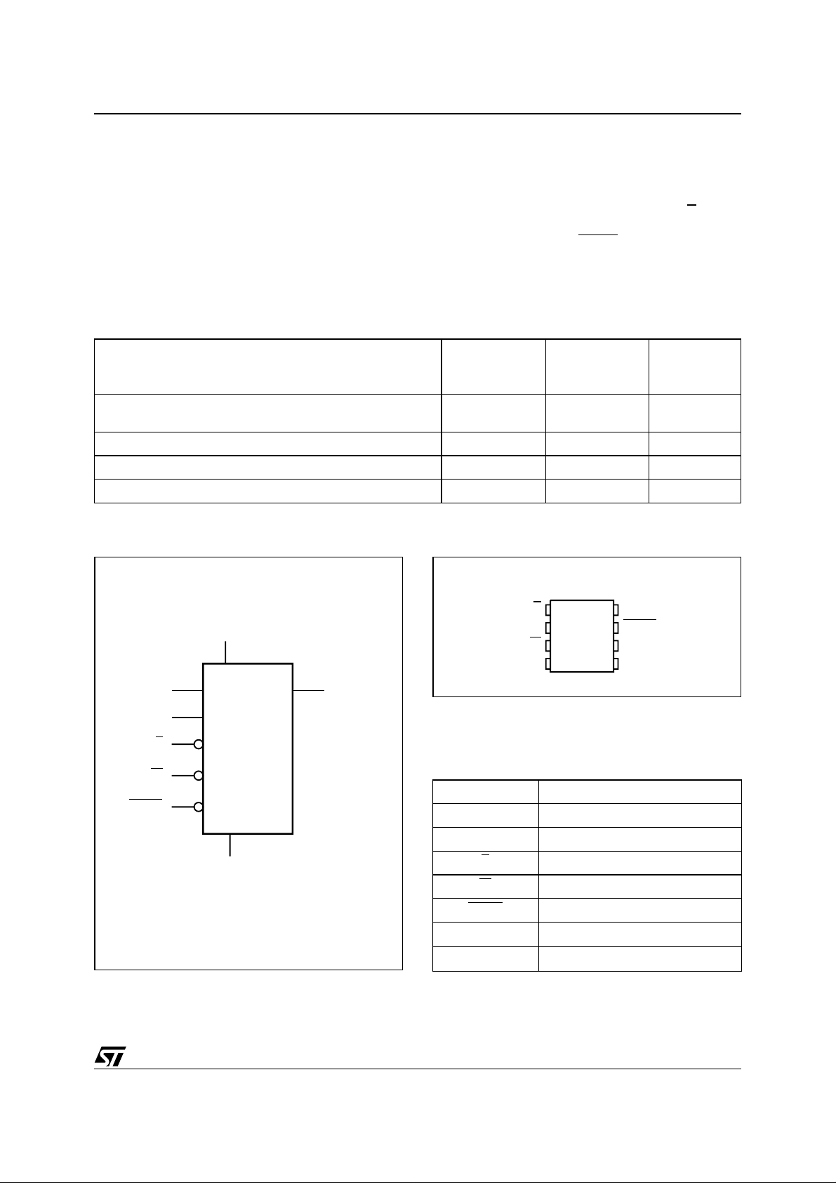
Figure 2. Logic Diagram Figure 3. 8 Pin Package Connections
M95xxx
SV
W
HOLD
1
W
SS
2
3
4
V
CC
D
C
S
M95xxx
Q
Note: 1. See PACKAGE MECHANICAL section for package di-
mensions and how to identify pin-1.
2. NC, Not Connected.
Table 3. Signal Names
C Serial Clock
D Serial data Input
Q Serial data Output
V
SS
AI01789C
S
W
HOLD
V
CC
V
SS
Chip Select
Write Protect
Hold
Supply Voltage
Ground
AI01790D
8
CC
HOLDQ
7
C
6
DV
5
5/42

M95640, M95320
SIGNAL DESCRIPTION
During all operations, VCC must be held stable and
within the specified valid range: V
(max).
V
CC
All of the input and output signals must be held
High or Low (according to voltages of V
or VOL, as specified in Table 16. to Table 20.).
These signals are described next.
Serial Data Output (Q). This output signal is
used to transfer data serially out of the device.
Data is shifted out on the falling edge of Serial
Clock (C).
Serial Data Input (D). This in put si gna l is used to
transfer data serially into the device. It receives instructions, addresse s, and the data to b e written.
Values are latched on the rising edge of Serial
Clock (C).
Serial Clock (C). This input signal provides the
timing of the serial interface. Instructions, addresses, or data present at Serial Data Input (D) are
latched on the rising edge of Serial Clock (C). Data
on Serial Data Output (Q) changes after the falling
edge of Serial Clock (C).
Chip Select (S
). When this input signal is High,
the device is des elected and Serial Data Out put
(min) to
CC
, VOH, V
IH
(Q) is at high impedance. Unless an internal Write
cycle is in progress, the device will be in the Standby Power mode. Driving Chip Se lect (S
lects the device, placing it in the Active Power
mode.
IL
After Power-up, a falling edge on Chip Sel ect (S
is required prior to the start of any instruction.
Hold (HOLD
). The Hold (HOLD) signal is used to
pause any serial c ommunicatio ns with the device
without deselecting the device.
During the Hold condition, the S erial Data Output
(Q) is high impedance, and Serial Data Input (D )
and Serial Clock (C) are Don’t Care.
To start the Hold condition, the device must be selected, with Chip Select (S
Write Protect (W
). The main purpose of this in-
) driven Low.
put signal is to freeze the size of the area of memory that is protected against Write instru ctio ns (a s
specified by the values in the BP1 and BP0 bits of
the Status Register).
This pin must b e driven either High or Low, and
must be stable during all write operations.
) Low se-
)
6/42
CONNECTING TO THE SPI BUS
These devices are fully compatible with the SPI
protocol.
All instructions, addresses and input data bytes
are shifted in to the device, most significant bit
first. The Serial Data Input (D) i s sampled o n the
first rising edge of the S erial Clock (C) a fter Chip
Select (S
) goes Low.
All output data bytes are shifted out of the device,
most significant bit first. The Serial Data Output
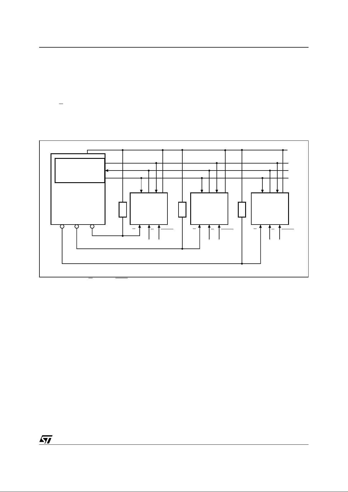
Figure 4. Bus Master and Memory Devices on the SPI Bus
SPI Interface with
(CPOL, CPHA) =
(0, 0) or (1, 1)
Bus Master
(ST6, ST7, ST9,
ST10, Others)
CS3 CS2 CS1
SDO
SDI
SCK
CQD
RRR
SPI Memory
Device
(Q) is latched on the first fa ll ing edge of the Serial
Clock (C) after the instruct ion (such as the Read
from Memory Array and Read S tatus Register in structions) have been clocked into the device.
Figure 4. shows three devices, connected to an
MCU, on a SPI bus. Only one device is selected at
a time, so only one device drives the S erial Data
Output (Q) line at a tim e, a ll th e others being high
impedance.
V
CC
CQD
SPI Memory
Device
M95640, M95320
V
CC
V
CC
CQD
SPI Memory
Device
V
CC
S
Note: The Write Protect (W) and Hold (HOLD) signals should be driven, High or Low as appropriat e.
HOLD
W
S
HOLD
W
S
W
AI03746e
HOLD
7/42

M95640, M95320
SPI Modes
These devices ca n be driv en by a m icrocontr oller
with its SPI peripheral runnin g in either of the two
following modes:
– CPOL=0, CPHA=0
– CPOL=1, CPHA=1
For these two modes, inpu t data is latched in on
the rising edge of Serial Clock (C), and output data
Figure 5. SPI Modes Supported
CPHA
CPOL
0
0
1
1
C
C
D
Q
MSB
is available from the falling edge of Serial Clock
(C).
The difference between the two modes, as shown
in Figure 5., is the clock polarity when the bus
master is in Stan d-by mode and not transferring
data:
– C remains at 0 for (CPOL=0, CPHA=0)
– C remains at 1 for (CPOL=1, CPHA=1)
MSB
AI01438B
8/42

OPERATING FEATURES
Power-Up
When the power supply is turned on, V
from V
During this time, the Ch ip Select (S
lowed to follow the V
to VCC.
SS
) must be al-
voltage. It must not be al-
CC
lowed to float, but should be connected to V
a suitable pull-up resistor.
As a built in safety feature, Chip Select (S
sensitive as well as level sensitive. After Powerup, the device does not become selected until a
falling edge has first been detected on Chip Select
(S
). This ensures that Chip Select (S) must have
been High, prior to going Low to star t the first operation.
Power On Reset: V
Lock-Out Write Protect
CC
In order to prevent inadvertent Write operations
during Power-up, each device include a Power On
Reset (POR) circuit. At Power-up, the dev ice will
not respond to any instruction until V
reached the Power On Reset threshold voltage.
This threshold is lower than the V
min operating
CC
voltage defined in Tables 10, 11, 12 and 13.
Similarly, as soon as V
drops from the normal
CC
operating voltage, below the Power On Reset
threshold voltage, the dev ice stops respondi ng to
any instruction sent to it.
Prior to selecting and issuing instructions to the
memory, a valid stable V
voltage must be ap-
CC
plied. This voltage must remain stable and valid
until the end of the transmissi on of the instruc tion
and, for a Write in struction, until the complet ion o
the internal write cycle (t
).
W
Power-down
At Power-down, the device must be deselected.
Chip Select (S
voltage applied on V
) should be allowed to follow the
.
CC
rises
CC
via
CC
) is edge
has
CC
M95640, M95320
Active Power and Standby Power Modes
When Chip Select (S
ed, and in the Active Power mode. The device
consumes I
CC
20..
When Chip Sel ec t (S
lected. If an Erase/Writ e cycle is not currently in
progress, the device then goe s in to the Standby
Power mode, and the device consump tion drops
to I
.
CC1
Hold Condition
The Hold ( HO LD
rial communications with the device without resetting the clocking sequence.
During the Hold condition, the S erial Data Output
(Q) is high impedance, and Serial Data Input (D )
and Serial Clock (C) are Don’t Care.
To enter the Hold condition, th e device must be
selected, with Chip Select (S
Normally, th e device i s kept sele cted, for the whole
duration of the Hold condition. Deselecting the device while it is in the Hold condition, has the effect
of resetting the state of the device, and this mechanism can be us ed if it is req uired to reset any pr ocesses that had been in progress.
The Hold condition starts when the Hol d (HOLD
signal is driven Low at the same time as Serial
Clock (C) already being Low (as shown in Figure
6.).
The Hold condition ends wh en the Hold (HOLD
signal is driven High at the same time as Serial
Clock (C) already being Low.
Figure 6. also shows what happens if the rising
and falling edges are not timed to coincide with
Serial Clock (C) being Low.
) is Low, the device is se lec t-
, as specified in Tabl e 16. to Table
) is High, the d ev ice is de se -
) signal is used to pau se a ny se -
) Low.
)
)
9/42

M95640, M95320
Figure 6. Hold Condition Activation
C
HOLD
Hold
Condition
Status Register
Figure 7. shows the position of the Status Register
in the control logic of the device. The Statu s Register contains a number of status and co ntrol bits
that can be read or set (as appropriate) by specific
instructions.
WIP bit. The Write In Progress (WIP) bit indicates
whether the memory is busy with a Write or Write
Status Register cycle.
WEL bit. The Write Enable Latch (WE L) bit indicates the status of the internal Write Enable Latch.
BP1, BP0 bits. The Block Protect (BP1, BP0) bits
are non-volatile. They define the size of the area to
be software protected against Write instructions.
SRWD bit. The Status Register Write Disable
(SRWD) bit is operated in conjunction with the
Write Protect (W
) signal. The Status Register
Write Disable (SRWD) bi t and Write Protect (W
signal allow the device to b e put in the Hardware
Protected mode. In this mode, the non-volatile bits
of the Status Register (SRWD, BP1, BP0) become
read-only bits.
Table 4. Status Register Format
b7 b0
SRWD 0 0 0 BP1 BP0 WEL WIP
Status Register Write Protect
Block Protect Bits
Write Enable Latch Bit
Write In Progress Bit
Hold
Condition
Data Protection and Protocol Control
Non-volatile memory devices can be used in environments that are particularly noisy, and within applications that could experience problems if
memory bytes are corrupted. Consequently, the
device features the following data protection
mechanisms:
■ Write and Write Status Register instructions
are checked that they consist of a number of
clock pulses that is a multiple of eight, before
they are accepted for execution.
■ All instructions that modify data must be
preceded by a Write Enable (WREN)
instruction to set the Write Enable Latch
(WEL) bit. This bit is returned to its reset state
by the following events:
– Power-up
)
– Write Disable (WRDI) instruction
completion
– Write Status Register (WRSR) instruction
completion
– Write (WRITE) instruction completion
■ The Block Protect (BP1, BP0) bits allow part of
the memory to be configured as read-only.
This is the Software Protected Mode (SPM).
■ The Write Protect (W) signal allows the Block
Protect (BP1, BP0) bits to be protected. This is
the Hardware Protected Mode (HPM).
For any instruction to be accepted, and executed,
Chip Select (S
) must be driven High after the rising
edge of Serial Clock (C) for the last bit of the instruction, and before the next rising edge of Serial
Clock (C).
Two points need to be noted in the previous sentence:
AI02029D
10/42
M95640, M95320
– The ‘last bit of the instruction’ can be the
eighth bit of the instruction code, or the eighth
bit of a data byte, depending on the instruction
– The ‘next rising edge of Serial Clock (C)’ might
(or might not) be the next bus transaction for
some other device on the SPI bus.
(except for Read Status Register (RDSR) and
Read (READ) instructions).
Table 5. Write-Protected Block Size
Status Register Bits
BP1 BP0
Protected Block
0 0 none none none
0 1 Upper quarter 1800h - 1FFFh 0C00h - 0FFFh
1 0 Upper half 1000h - 1FFFh 0800h - 0FFFh
1 1 Whole memory 0000h - 1FFFh 0000h - 0FFFh
M95640, M95640-W,
M95640-R, M95640-S
Array Addresses Protected
M95320, M95320-W,
M95320-R, M95320-S
11/42
M95640, M95320
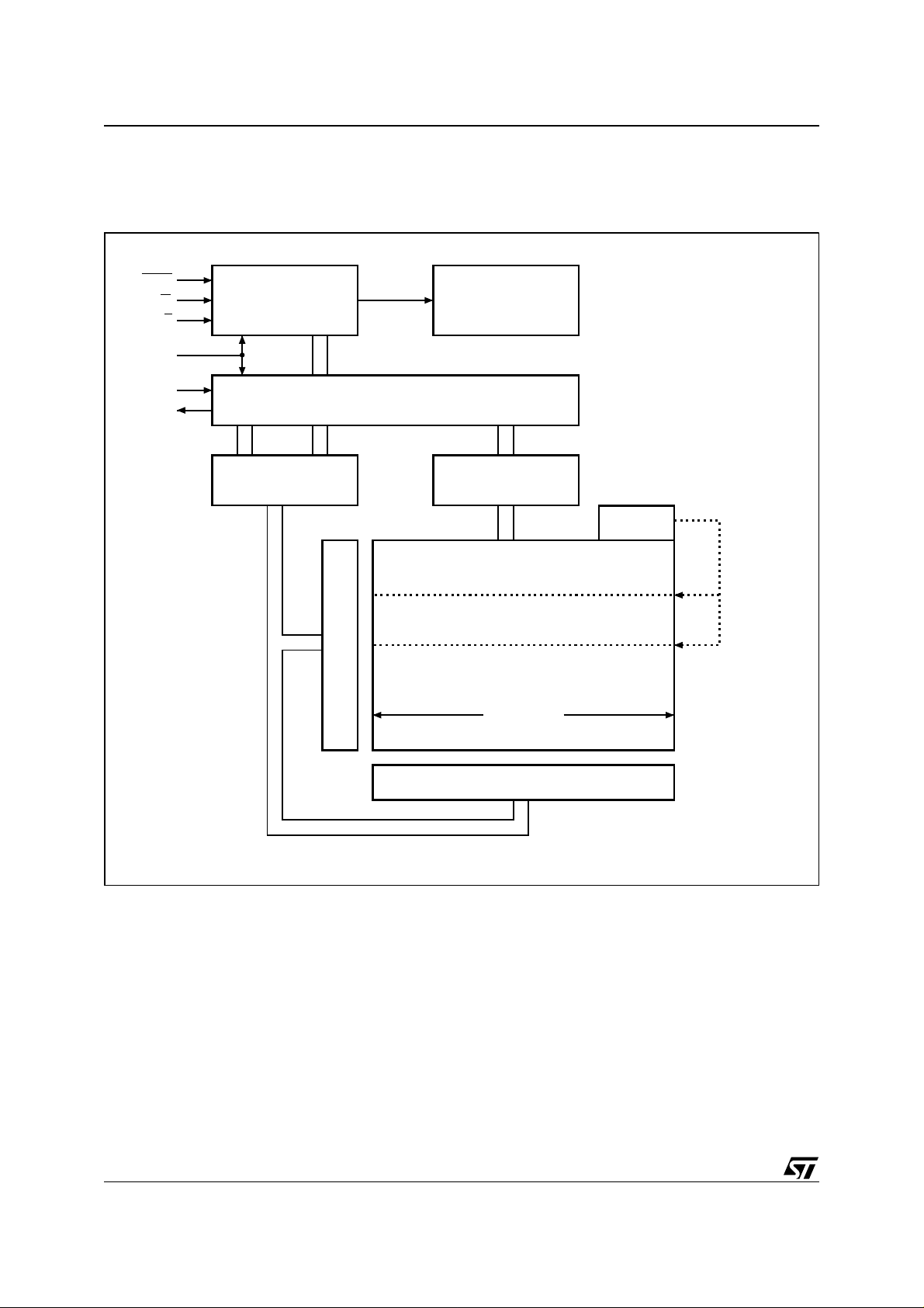
MEMORY ORGANIZATION
The memory is organized as shown in Figure 7..
Figure 7. Block Diagram
HOLD
W
S
C
D
Q
Control Logic
I/O Shift Register
Address Register
and Counter
Y Decoder
High Voltage
Generator
Data
Register
1 Page
Status
Register
Size of the
Read only
EEPROM
area
12/42
X Decoder
AI01272C

INSTRUCTIONS
Each instruction star ts wi th a singl e- by te cod e, a s
summarized in Table 6..
If an invalid instruct ion is sent ( one not contain ed
in Table 6.), the device automaticall y des elect s it self.
M95640, M95320
Table 6. Instruction Set
Instruc
tion
WREN Write Enable 0000 0110
WRDI Write Disable 0000 0100
RDSR Read Status Register 0000 0101
WRSR Write Status Register 0000 0001
READ Read from Memory Array 0000 0011
WRITE Write to Memory Array 0000 0010
Description
Instruction
Format
13/42
 Loading...