


查询M95128-BN3TG供应商
256Kbit and 128Kbit Serial SPI Bus EEPROM
FEAT URES SUMMARY
■ Compatible with SPI Bus Serial Interfa c e
(Positive Clock SPI Modes)
■ Single Supply Voltage:
– 4.5 to 5.5V for M95xxx
– 2.5 to 5.5V for M95xxx-W
– 1.8 to 5.5V for M95xxx-R
■ High Speed
– 10MHz Clock Rate, 5ms Write Time
■ Status Register
■ Hardware Protection of the Status Register
■ BYTE and PAGE WRITE (up to 64 Bytes)
■ Self-Timed Programming Cycle
■ Adjustable Size Read-Only EEPROM Area
■ Enhanced ESD Protection
■ More than 100000 Erase/Write Cycles
■ More than 40-Year Data Retention
M95256
M95128
With High Speed Clock
Figure 1. Packages
8
1
PDIP8 (BN)
0.25 mm frame
8
Table 1. Product List
Reference Part Number
M95256
M95128
M95256
M95256-W
M95256-R
M95128
M95128-W
M95128-R
1
SO8 (MN)
150 mil width
8
1
SO8 (MW)
200 mil width
TSSOP8 (DW)
169 mil width
1/39October 2004

M95256, M95128
TABLE OF CONTENTS
FEATURES SUMMARY . . . . . . . . . . . . . . . . . . . . . . . . . . . . . . . . . . . . . . . . . . . . . . . . . . . . . . . . . . . . . 1
Table 1. Product List . . . . . . . . . . . . . . . . . . . . . . . . . . . . . . . . . . . . . . . . . . . . . . . . . . . . . . . . . . . . 1
Figure 1. Packages. . . . . . . . . . . . . . . . . . . . . . . . . . . . . . . . . . . . . . . . . . . . . . . . . . . . . . . . . . . . . . 1
Figure 2. Logic Diagram . . . . . . . . . . . . . . . . . . . . . . . . . . . . . . . . . . . . . . . . . . . . . . . . . . . . . . . . . . 5
Figure 3. DIP, SO and TSSOP Connections . . . . . . . . . . . . . . . . . . . . . . . . . . . . . . . . . . . . . . . . . . 5
Table 2. Signal Names . . . . . . . . . . . . . . . . . . . . . . . . . . . . . . . . . . . . . . . . . . . . . . . . . . . . . . . . . . 5
SIGNAL DESCRIPTION . . . . . . . . . . . . . . . . . . . . . . . . . . . . . . . . . . . . . . . . . . . . . . . . . . . . . . . . . . . . . 6
Serial Data Output (Q). . . . . . . . . . . . . . . . . . . . . . . . . . . . . . . . . . . . . . . . . . . . . . . . . . . . . . . . . . . . 6
Serial Data Input (D) . . . . . . . . . . . . . . . . . . . . . . . . . . . . . . . . . . . . . . . . . . . . . . . . . . . . . . . . . . . . . 6
Serial Clock (C) . . . . . . . . . . . . . . . . . . . . . . . . . . . . . . . . . . . . . . . . . . . . . . . . . . . . . . . . . . . . . . . . .6
Chip Select (S) . . . . . . . . . . . . . . . . . . . . . . . . . . . . . . . . . . . . . . . . . . . . . . . . . . . . . . . . . . . . . . . . . 6
Hold (HOLD) . . . . . . . . . . . . . . . . . . . . . . . . . . . . . . . . . . . . . . . . . . . . . . . . . . . . . . . . . . . . . . . . . . . 6
Write Protect (W). . . . . . . . . . . . . . . . . . . . . . . . . . . . . . . . . . . . . . . . . . . . . . . . . . . . . . . . . . . . . . . . 6
CONNECTING TO THE SPI BUS . . . . . . . . . . . . . . . . . . . . . . . . . . . . . . . . . . . . . . . . . . . . . . . . . . . . . . 7
Figure 4. Bus Master and Memory Devices on the SPI Bus. . . . . . . . . . . . . . . . . . . . . . . . . . . . . . . 7
SPI Modes . . . . . . . . . . . . . . . . . . . . . . . . . . . . . . . . . . . . . . . . . . . . . . . . . . . . . . . . . . . . . . . . . . . . 8
Figure 5. SPI Modes Supported . . . . . . . . . . . . . . . . . . . . . . . . . . . . . . . . . . . . . . . . . . . . . . . . . . . . 8
OPERATING FEATURES. . . . . . . . . . . . . . . . . . . . . . . . . . . . . . . . . . . . . . . . . . . . . . . . . . . . . . . . . . . . 9
Power-up . . . . . . . . . . . . . . . . . . . . . . . . . . . . . . . . . . . . . . . . . . . . . . . . . . . . . . . . . . . . . . . . . . . . . 9
Power On Reset: VCC Lock-Out Write Protect. . . . . . . . . . . . . . . . . . . . . . . . . . . . . . . . . . . . . . . 9
Power-down. . . . . . . . . . . . . . . . . . . . . . . . . . . . . . . . . . . . . . . . . . . . . . . . . . . . . . . . . . . . . . . . . . . 9
Active Power and Standby Power Modes. . . . . . . . . . . . . . . . . . . . . . . . . . . . . . . . . . . . . . . . . . . 9
Hold Condition. . . . . . . . . . . . . . . . . . . . . . . . . . . . . . . . . . . . . . . . . . . . . . . . . . . . . . . . . . . . . . . . . 9
Figure 6. Hold Condition Activation. . . . . . . . . . . . . . . . . . . . . . . . . . . . . . . . . . . . . . . . . . . . . . . . . . 9
Status Register . . . . . . . . . . . . . . . . . . . . . . . . . . . . . . . . . . . . . . . . . . . . . . . . . . . . . . . . . . . . . . . 10
WIP bit. . . . . . . . . . . . . . . . . . . . . . . . . . . . . . . . . . . . . . . . . . . . . . . . . . . . . . . . . . . . . . . . . . . . . . . 1 0
WEL bit . . . . . . . . . . . . . . . . . . . . . . . . . . . . . . . . . . . . . . . . . . . . . . . . . . . . . . . . . . . . . . . . . . . . . . 1 0
BP1, BP0 bits . . . . . . . . . . . . . . . . . . . . . . . . . . . . . . . . . . . . . . . . . . . . . . . . . . . . . . . . . . . . . . . . . 10
SRWD bit. . . . . . . . . . . . . . . . . . . . . . . . . . . . . . . . . . . . . . . . . . . . . . . . . . . . . . . . . . . . . . . . . . . . . 10
Table 3. Status Register Format . . . . . . . . . . . . . . . . . . . . . . . . . . . . . . . . . . . . . . . . . . . . . . . . . . 10
Data Protection and Protocol Control . . . . . . . . . . . . . . . . . . . . . . . . . . . . . . . . . . . . . . . . . . . . . 10
Table 4. Write-Protected Block Size . . . . . . . . . . . . . . . . . . . . . . . . . . . . . . . . . . . . . . . . . . . . . . .10
MEMORY ORGANIZATION . . . . . . . . . . . . . . . . . . . . . . . . . . . . . . . . . . . . . . . . . . . . . . . . . . . . . . . . . 11
Figure 7. Block Diagram . . . . . . . . . . . . . . . . . . . . . . . . . . . . . . . . . . . . . . . . . . . . . . . . . . . . . . . . . 11
INSTRUCTIONS . . . . . . . . . . . . . . . . . . . . . . . . . . . . . . . . . . . . . . . . . . . . . . . . . . . . . . . . . . . . . . . . . . 12
Table 5. Instruction Set . . . . . . . . . . . . . . . . . . . . . . . . . . . . . . . . . . . . . . . . . . . . . . . . . . . . . . . . . 12
Write Enable (WREN) . . . . . . . . . . . . . . . . . . . . . . . . . . . . . . . . . . . . . . . . . . . . . . . . . . . . . . . . . . 13
Figure 8. Write Enable (WREN) Sequence. . . . . . . . . . . . . . . . . . . . . . . . . . . . . . . . . . . . . . . . . . . 13
2/39

M95256, M95128
Write Disable (WRDI) . . . . . . . . . . . . . . . . . . . . . . . . . . . . . . . . . . . . . . . . . . . . . . . . . . . . . . . . . . . 13
Figure 9. Write Disable (WRDI) Sequence. . . . . . . . . . . . . . . . . . . . . . . . . . . . . . . . . . . . . . . . . . . 13
Read Status Register (RDSR). . . . . . . . . . . . . . . . . . . . . . . . . . . . . . . . . . . . . . . . . . . . . . . . . . . . 14
WIP bit. . . . . . . . . . . . . . . . . . . . . . . . . . . . . . . . . . . . . . . . . . . . . . . . . . . . . . . . . . . . . . . . . . . . . . . 1 4
WEL bit . . . . . . . . . . . . . . . . . . . . . . . . . . . . . . . . . . . . . . . . . . . . . . . . . . . . . . . . . . . . . . . . . . . . . . 1 4
BP1, BP0 bits . . . . . . . . . . . . . . . . . . . . . . . . . . . . . . . . . . . . . . . . . . . . . . . . . . . . . . . . . . . . . . . . . 14
SRWD bit. . . . . . . . . . . . . . . . . . . . . . . . . . . . . . . . . . . . . . . . . . . . . . . . . . . . . . . . . . . . . . . . . . . . . 14
Figure 10.Read Status Register (RDSR) Sequence . . . . . . . . . . . . . . . . . . . . . . . . . . . . . . . . . . . . 14
Write Status Register (WRSR) . . . . . . . . . . . . . . . . . . . . . . . . . . . . . . . . . . . . . . . . . . . . . . . . . . . 15
Table 6. Protection Modes . . . . . . . . . . . . . . . . . . . . . . . . . . . . . . . . . . . . . . . . . . . . . . . . . . . . . . . 15
Figure 11.Write Status Register (WRSR) Sequence. . . . . . . . . . . . . . . . . . . . . . . . . . . . . . . . . . . . 16
Read from Memory Array (READ) . . . . . . . . . . . . . . . . . . . . . . . . . . . . . . . . . . . . . . . . . . . . . . . . 17
Figure 12.Read from Memory Array (READ) Sequen ce . . . . . . . . . . . . . . . . . . . . . . . . . . . . . . . . . 17
Write to Memory Array (WRITE). . . . . . . . . . . . . . . . . . . . . . . . . . . . . . . . . . . . . . . . . . . . . . . . . .18
Figure 13.Byte Write (WRITE) Sequence . . . . . . . . . . . . . . . . . . . . . . . . . . . . . . . . . . . . . . . . . . . . 18
Figure 14.Page Write (WRITE) Sequence . . . . . . . . . . . . . . . . . . . . . . . . . . . . . . . . . . . . . . . . . . . 19
POWER-UP AND DELIVERY STATE . . . . . . . . . . . . . . . . . . . . . . . . . . . . . . . . . . . . . . . . . . . . . . . . . . 20
Power-up State . . . . . . . . . . . . . . . . . . . . . . . . . . . . . . . . . . . . . . . . . . . . . . . . . . . . . . . . . . . . . . . 20
Initial Delivery State . . . . . . . . . . . . . . . . . . . . . . . . . . . . . . . . . . . . . . . . . . . . . . . . . . . . . . . . . . . 20
MAXIMUM RATING. . . . . . . . . . . . . . . . . . . . . . . . . . . . . . . . . . . . . . . . . . . . . . . . . . . . . . . . . . . . . . . . 21
Table 7. Absolute Maximum Ratings. . . . . . . . . . . . . . . . . . . . . . . . . . . . . . . . . . . . . . . . . . . . . . . 21
DC AND AC PARAMETERS. . . . . . . . . . . . . . . . . . . . . . . . . . . . . . . . . . . . . . . . . . . . . . . . . . . . . . . . . 22
Table 8. Operating Conditions (M95xxx) . . . . . . . . . . . . . . . . . . . . . . . . . . . . . . . . . . . . . . . . . . . . 22
Table 9. Operating Conditions (M95xxx-W). . . . . . . . . . . . . . . . . . . . . . . . . . . . . . . . . . . . . . . . . . 22
Table 10. Operating Conditions (M95xxx-R) . . . . . . . . . . . . . . . . . . . . . . . . . . . . . . . . . . . . . . . . . . 22
Table 11. AC Measurement Conditions. . . . . . . . . . . . . . . . . . . . . . . . . . . . . . . . . . . . . . . . . . . . . . 23
Figure 15.AC Measurement I/O Waveform. . . . . . . . . . . . . . . . . . . . . . . . . . . . . . . . . . . . . . . . . . . 23
Table 12.Capacitance. . . . . . . . . . . . . . . . . . . . . . . . . . . . . . . . . . . . . . . . . . . . . . . . . . . . . . . . . . . 23
Table 13. DC Characteristics (M95xxx, Device Grade 6) . . . . . . . . . . . . . . . . . . . . . . . . . . . . . . . . 24
Table 14. DC Characteristics (M95xxx, Device Grade 3) . . . . . . . . . . . . . . . . . . . . . . . . . . . . . . . . 24
Table 15. DC Characteristics (M95xxx-W, Device Grade 6). . . . . . . . . . . . . . . . . . . . . . . . . . . . . . 24
Table 16. DC Characteristics (M95xxx-W, Device Grade 3). . . . . . . . . . . . . . . . . . . . . . . . . . . . . . 25
Table 17. DC Characteristics (M95xxx-R). . . . . . . . . . . . . . . . . . . . . . . . . . . . . . . . . . . . . . . . . . . . 25
Table 18. AC Characteristics (M95xxx, Device Grade 6) . . . . . . . . . . . . . . . . . . . . . . . . . . . . . . . . 26
Table 19. AC Characteristics (M95xxx, Device Grade 3) . . . . . . . . . . . . . . . . . . . . . . . . . . . . . . . . 27
Table 20. AC Characteristics (M95xxx-W, Device Grade 6) . . . . . . . . . . . . . . . . . . . . . . . . . . . . . . 28
Table 21. AC Characteristics (M95xxx-W, Device Grade 3) . . . . . . . . . . . . . . . . . . . . . . . . . . . . . . 29
Table 22. AC Characteristics (M95xxx-R) . . . . . . . . . . . . . . . . . . . . . . . . . . . . . . . . . . . . . . . . . . . . 30
Figure 16.Serial Input Timing . . . . . . . . . . . . . . . . . . . . . . . . . . . . . . . . . . . . . . . . . . . . . . . . . . . . . 31
Figure 17.Hold Timing. . . . . . . . . . . . . . . . . . . . . . . . . . . . . . . . . . . . . . . . . . . . . . . . . . . . . . . . . . . 31
Figure 18.Output Timing . . . . . . . . . . . . . . . . . . . . . . . . . . . . . . . . . . . . . . . . . . . . . . . . . . . . . . . . . 32
PACKAGE MECHANICAL . . . . . . . . . . . . . . . . . . . . . . . . . . . . . . . . . . . . . . . . . . . . . . . . . . . . . . . . . . 33
3/39

M95256, M95128
Figure 19.PDIP8 – 8 pin Plastic DIP, 0.25mm lead frame, Package Outline . . . . . . . . . . . . . . . . . 33
Table 23. PDIP8 – 8 pin Plastic DIP, 0.25mm lead frame, Package Mechanical Data. . . . . . . . . . 33
Figure 20.SO8 narrow – 8 lead Plastic Small Outline, 150 mils body width, Package Outline . . . . 34
Table 24. SO8 narrow – 8 lead Plastic Small Outline, 150 mils body width, Package Mechanical Data
34
Figure 21.SO8 wide – 8 lead Plastic Small Outline, 200 mils body width, Package Outline. . . . . . 35
Table 25. SO8 wide – 8 lead Plastic Small Outline, 200 mils body width, Package Mechanical Data
35
Figure 22.TSSOP8 – 8 lead Thin Shrink Small Outline, Package Outline . . . . . . . . . . . . . . . . . . . 36
Table 26. TSSOP8 – 8 lead Thin Shrink Small Outline, Package Mechanica l Data . . . . . . . . . . . . 36
PART NUMBERING . . . . . . . . . . . . . . . . . . . . . . . . . . . . . . . . . . . . . . . . . . . . . . . . . . . . . . . . . . . . . . . 37
Table 27.Ordering Information Scheme . . . . . . . . . . . . . . . . . . . . . . . . . . . . . . . . . . . . . . . . . . . . . 37
REVISION HISTORY. . . . . . . . . . . . . . . . . . . . . . . . . . . . . . . . . . . . . . . . . . . . . . . . . . . . . . . . . . . . . . . 38
Table 28. Document Revision History. . . . . . . . . . . . . . . . . . . . . . . . . . . . . . . . . . . . . . . . . . . . . . . 38
4/39

M95256, M95128
SUMMARY DESCRIPTION
These electrically erasable programmable memory (EEPROM) devices are accessed by a high
speed SPI-compatible bus. The memory array is
organized as 32768 x 8 bit (M95256) and 16384 x
8 bit (M95128).
The device is accessed by a simple serial interface
that is SPI-compatible. The bus signa ls are C, D
and Q, as shown in Table 2. and Figu re 2..
The device is selected when Chip Select (S
en Low. Communications with the devi ce can be
interrupted using Hold (HOLD
).
Figure 2. Logic Diagram
V
CC
D
C
S
W
HOLD
M95xxx
) is tak-
Q
Figure 3. DIP, SO and TSSOP Connections
M95xxx
SV
1
2
W
3
4
SS
Note: See PACKAGE MECHANICAL section for package dimen-
sions, and how to identify pi n-1.
8
7
6
5
AI01790D
CC
HOLDQ
C
DV
Table 2. Signal Names
C Serial Clock
D Serial Data Input
Q Serial Data Output
S Chip Select
Write Protect
W
HOLD
Hold
V
CC
V
SS
AI01789C
V
SS
Supply Voltage
Ground
5/39

M95256, M95128
SIGNAL DESCRIPTION
During all operations, VCC must be held stable and
within the specified valid range: V
(max).
V
CC
All of the input and out put signals must be held
High or Low (according to voltages of V
or VOL, as specified in Table 13. to Table 17.).
These signals are described next.
Serial Data Output (Q). This output signal is
used to transfer data serially out of the device.
Data is shifted out on the falling edge of Serial
Clock (C).
Serial Data Input (D). This input signal is used to
transfer data serially into the device. It receives instructions, addresses, and the data to be written.
Values are latched on the rising edge of Serial
Clock (C).
Serial Clock (C). This input signal provides the
timing of the serial interface. Instructions, addresses, or data present at Serial Data Input (D) are
latched on the rising edge of Serial Clock (C). Data
on Serial Data Output (Q) changes after the falling
edge of Serial Clock (C).
Chip Select (S
). When this input signal is High,
the device is des elected and Serial Data Ou tput
(min) to
CC
, VOH, V
IH
(Q) is at high impedance. Unless an internal Write
cycle is in progress, the device will be in the Standby Power mode. Drivi ng Chip Select ( S
lects the device, placing it in the Active Power
mode.
IL
After Power-up, a falling edge on Chip Select (S
is required prior to the start of any instruction.
Hold (HOLD
). The Hold (HOLD) signal is used to
pause any serial communications with the device
without deselecting the device.
During the Hold condition, the Serial Data Output
(Q) is high impedanc e, and Serial D ata Input (D)
and Serial Clock (C) are Don’t Care.
To start the Hold condition, the device must be selected, wit h Ch ip Select (S
Write Protect (W
). The main purpose of this in-
) driven Low.
put signal is to freeze the size of the area of memory that is protected against Write instructions (as
specified by the values in the BP1 and BP0 bits of
the Status Register).
This pin must be driven e ither High or Low, and
must be stable during all write instructions.
) Low se-
)
6/39

CONNECTI NG TO THE SPI BUS
These devices are fully compatible with the SPI
protocol.
All instructions, addresses and input data bytes
are shifted in to the device, most significant bit
first. The Serial Data Input (D) is sampled on the
first rising edge of the Serial Clock (C) after Chip
Selec t ( S
) goes Low.
All output data bytes are shifted out of the device,
most significant bit first. The Serial Data Output
Figure 4. Bus Master and Memory Devices on the SPI Bus
(Q) is latched on the first fa lling edge of the Serial
Clock (C) after the instruction (such as the Read
from Memory Array and Read Status Re gister instructions) have been clocked into the device.
Figure 4 . shows three devices, con nected to an
MCU, on a SPI bus. Only one device is selected at
a time, so only one de vice drives the Serial Data
Output (Q) line at a time, all the o thers be ing high
impedance.
M95256, M95128
SPI Interface with
(CPOL, CPHA) =
(0, 0) or (1, 1)
Bus Master
(ST6, ST7, ST9,
ST10, Others)
CS3 CS2 CS1
Note: The Write Protect (W) and Hold (HOLD) signals should be drive n, High or Low as appropriate.
SDO
SDI
SCK
CQD
SPI Memory
Device
S
CQD
SPI Memory
Device
HOLD
W
S
HOLD
W
CQD
SPI Memory
Device
S
W
AI03746D
HOLD
7/39

M95256, M95128
SPI Modes
These devices can be drive n by a microcont roller
with its SPI peripheral running in either of the two
following modes:
– CPOL=0, CPHA=0
– CPOL=1, CPHA=1
For these two modes, input data is latc hed in on
the rising edge of Serial Clock (C), and output data
Figure 5. SPI Mo de s S upported
CPHA
CPOL
0
0
1
1
C
C
D
Q
MSB
is avai lable from t he falling edge of S erial Clock
(C).
The difference between the two modes, as shown
in Figure 5., is the clock polarity when the bus
master is in Stand-by mode and not transferring
data:
– C remains at 0 for (CPOL=0, CPHA=0)
– C remains at 1 for (CPOL=1, CPHA=1)
MSB
AI01438B
8/39
OPERATING FEAT URES
Power-up
When the power supply is turned on, V
from V
During this time, the Chip Select (S
lowed to follow the V
to VCC.
SS
) must be al-
voltage. It must not be al-
CC
lowed to float, but should be connected to V
a suitable pull-up resistor.
As a built in safety feature, Chip Select (S
sensitive as well a s level sens itive. After P owerup, the device does not become s elected until a
falling edge has first been detected on Chip Select
). This ensures that Ch ip Select (S) must have
(S
been High, prior to going Low to start the first operation.
Power On Reset: V
Lock-Out Write Protect
CC
In order to prevent data corruption and inadvertent
Write instructions during Power-up, a Power On
Reset (POR) circuit is included. The internal reset
is held active until V
has reached the Power On
CC
Reset (POR) threshold voltage, and all operations
are disabled – the device will not respond to any
instruction. In the same way, when V
CC
the operating voltage, below the Power On Reset
(POR) threshold voltage, all operations are disabled and the device will not res pond to any instruction.
A stable and valid V
must be applied before ap-
CC
plying any logic signal.
Power-down
At Power-down, the device must be deselected.
Chip Select (S
voltage applied on V
) should be allowed to follow the
.
CC
Active Power and Standb y Power M ode s
When Chip Select (S
) is Low, the device is select-
ed, and in the Active Power mode. The device
rises
CC
via
CC
) is edge
drops from
M95256, M95128
consumes I
17..
When Chip Select (S
lected. If an Erase/Write cycle is not currently in
progress, the device then goes in to the Standby
Power mode, and the device cons umption drops
CC1
.
to I
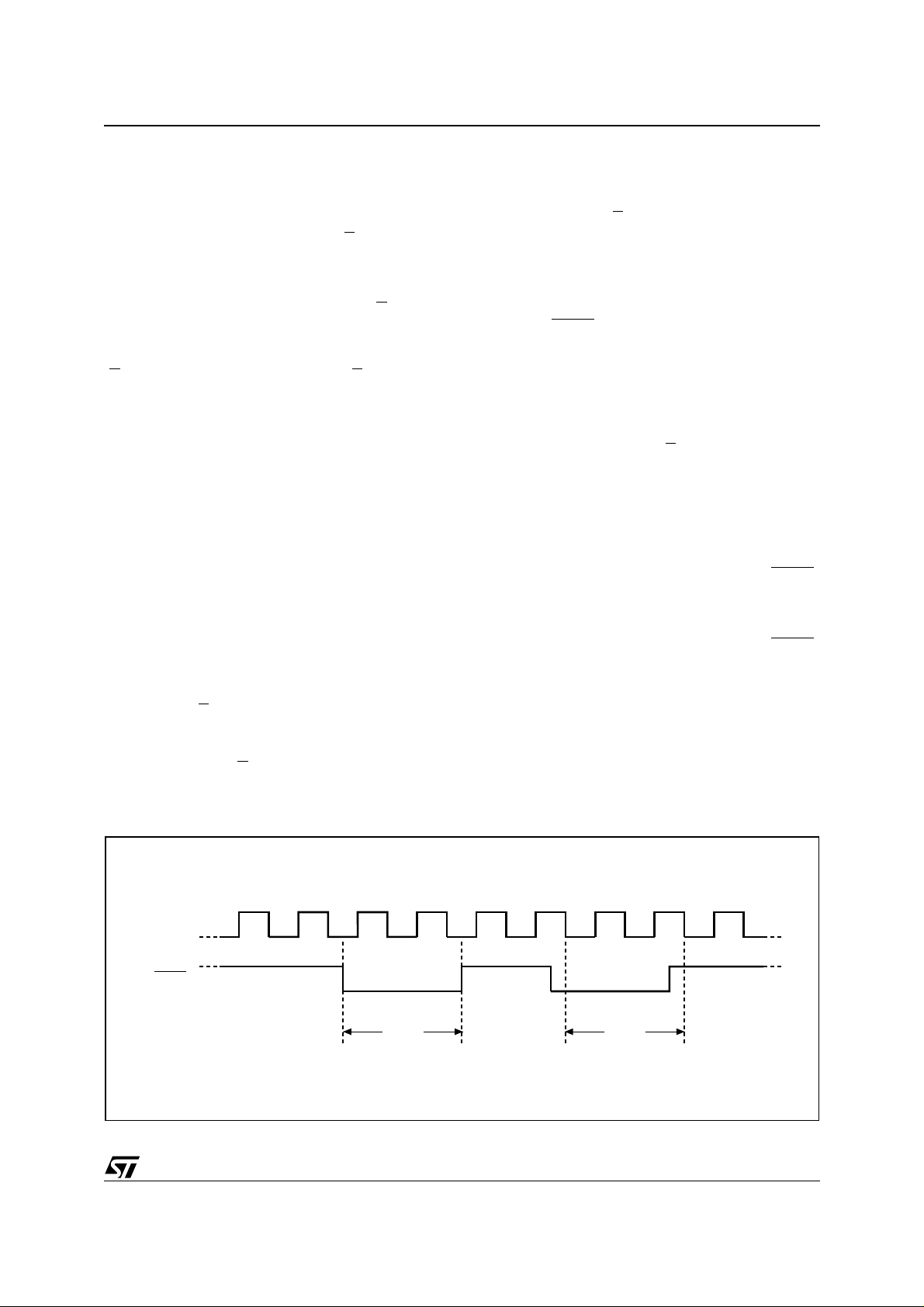
Hold Condition
The Hold (HOLD
rial communications with the device without resetting the clocking sequence.
During the Hold condition, the Serial Data Output
(Q) is high impedanc e, and Serial D ata Input (D)
and Serial Clock (C) are Don’t Care.
To enter the Hold condition, the device must be
selecte d, with Chip Selec t (S
Normally, the device is kept selected, for the whole
duration of the Hold condition. Deselecting the device while it is in the Hold condition, has the effect
of resetting the state of the device, and this mechanism can be used if it is required to reset any processes that had been in progress.
The Hold condition starts when the Hold (HOLD
signal is driven Low at the same time as Serial
Clock (C) already being Low (as shown in Figure
6.).
The Hold condition ends when the Hold (HOLD
signal is driven High at the same time as Serial
Clock (C) already being Low.
Figure 6 . also shows what happens if the rising
and falling edges are not timed to coincide with
Serial Clock (C) being Low.
, as specified in Table 13. to Table
CC
) is High, the device is dese-
) signal is used to pause any se-
) Low.
)
)
Figure 6. Hold Condition Activation
C
HOLD
Hold
Condition
Hold
Condition
AI02029D
9/39

M95256, M95128
Status Register
Figure 7. shows the position of the Status Register
in the control logic of the d evice. The Status Register contains a number of status and cont rol bits
that can be read or set (as appropriate) by specific
instructions.
WIP bit. The Write In Progress (WIP) bit indicates
whether the memory is busy with a Write or Write
Status Register cycle.
WEL bit. The Write Enable Latch (WEL) bit i ndicates the status of the internal Write Enable Latch.
BP1, BP0 bits. The Block Protect (BP1, BP0) bits
are non-volatile. They define the size of the area to
be software protected against Write instructions.
SRWD bit. The Status Register Write Disable
(SRWD) bit is operated in conjunction with the
Write Protect (W
) signal. The Status Register
Write Disable (SRWD) bit an d Write Protect (W
signal allow the device to be put in the Hardware
Protected mode. In this mode, the non-volatile bits
of the Status Register (SRWD, BP1, BP0) become
read-only bits.
Table 3. Status Register Format
b7 b0
SRWD 0 0 0 BP1 BP0 WEL WIP
Status Register Write Protect
Block Protect Bits
Write Enable Latch Bit
Write In Progress Bit
Data Protec ti on a n d Protocol Cont rol
Non-volatile memory devices can be used in environments that are particularly noisy, and within applications that could experience problems if
memory bytes are corrupted. Consequently, the
device features the following data protection
mechanisms:
■ Write and Write Status Register instructions
are checked that they consist of a number of
clock pulses that is a multiple of eight, before
they are accepted for execution.
■ All instructions that modify data must be
preceded by a Write Enable (WREN)
instruction to set the Write Enable Latch
(WEL) bit. This bit is returned to its reset state
by the following events:
– Power-up
– Write Disable (WRDI) instruction
completion
– Write Status Register (WRSR) instruction
completion
)
– Write (WRITE) instruction completion
■ The Block Protect (BP1, BP0) bits allow part of
the memory to be configured as read-only.
This is the Software Protected Mode (SPM).
■ The Write Protect (W) signal allows the Block
Protect (BP1, BP0) bits to be protected. This is
the Hardware Protected Mode (HPM).
For any instruction to be accepted, and e xe cuted,
Chip Select (S
) must be driven High after the rising
edge of Serial Clock (C) for the last bit of the instruction, and before the next rising edge of Serial
Clock (C).
Two points need to be no ted in the p revious sentence:
– The ‘last bit of the instruction’ can be the
eighth bit of the instruction code, or the eighth
bit of a data byte, depending on the instruction
(except for Read Status Register (RDSR) and
Read (READ) instructions).
– The ‘next rising edge of Serial Clock (C)’ might
(or might not) be the next bus transaction for
some other device on the SPI bus.
Table 4. Write-Protected Block Size
Status Register Bits
BP1 BP0 M95256 M95128
0 0 none none none
0 1 Upper quarter 6000h - 7FFFh 3000h - 3FFFh
1 0 Upper half 4000h - 7FFFh 2000h - 3FFFh
1 1 Whole memory 0000h - 7FFFh 0000h - 3FFFh
10/39
Protected Block
Array Addresses Protected

MEMOR Y ORGANIZ ATION
The memory is organized as shown in Figure 7..
Figure 7. Block Diagram
M95256, M95128
HOLD
W
S
C
D
Q
Control Logic
I/O Shift Register
Address Register
and Counter
Y Decoder
High Voltage
Generator
Data
Register
1 Page
Status
Register
Size of the
Read only
EEPROM
area
X Decoder
AI01272C
11/39

M95256, M95128
INSTRUCTIONS
Each instruction starts with a single-byte code, as
summarized in Table 5..
If an invalid instruction is s ent (one not con tained
in Table 5.), the device automatically deselects itself.
Table 5. Instruction Set
Instruc
tion
WREN Write Enable 0000 0110
WRDI Write Disable 0000 0100
RDSR Read Status Register 0000 0101
WRSR Write Status Register 0000 0001
READ Read from Memory Array 0000 0011
WRITE Write to Memory Array 0000 0010
Description
Instruction
Format
12/39

M95256, M95128
Write Enable (WREN)
The Write Enable Latch (WEL) bit must be set prior to each WRITE and WRSR instruction. The only
way to do this is to send a Write Enable instruction
to the device.
Figure 8. Write Enable (WREN) Sequence
S
0
C
D
High Impedance
Q
Write Disable (WRDI)
One way of resetting the Write Enable Latch
(WEL) bit is to send a Write Disable instruction to
the device.
As shown in Figure 9., to send this i nstruc tion t o
the devic e , C hip Select ( S
) is driven Low, and the
bits of the instruction byte are shifted in, on Serial
Data Input (D).
As shown in Figure 8., to send this instruction to
the devic e , C hip Select ( S
) is driven Low, and the
bits of the instruction byte are shifted in, on Serial
Data Input (D). The device then enters a wait
state. It waits for a the device to be deselected, by
Chip Selec t ( S
21 34567
Instruction
) being driven High.
AI02281E
The device then enters a wait state. It waits for a
the device to be deselected, by Chip Select (S
ing driven High.
The Write Enable Latch (WEL) bit, in fact, becomes reset by any of the following events:
–Power-up
– WRDI instruction execution
– WRSR instruction completion
– WRITE instruction completion.
) be-
Figure 9. Write Disable (WRDI) Sequence
S
C
D
Q
0
21 34567
Instruction
High Impedance
AI03750D
13/39

M95256, M95128
Read Status Register (RDSR)
The Read Status Register (RDSR) instruction allows the Status Register to be read. The Status
Register may be read at any time, even while a
Write or Write Statu s Register cycl e is i n progress .
When one of these cycles is in progress, it is recommended to check the Write In Prog ress (WIP)
bit before sending a new instruction to the device.
It is also possible to read the Status Register continuously, as shown in Figure 10..
The status and control bits of t he Status Register
are as follows:
WIP bit. The Write In Progress (WIP) bit indicates
whether the memory is busy with a Write or Write
Status Register cycle. When set to 1, such a cycle
is in progress, when reset to 0 no such cycle is in
progress.
WEL bit. The Write Enable Latch (WEL) bit i ndicates the status of the internal Write Enable Latch.
When set to 1 the internal Write Enable Latch is
set, when set to 0 t he i nternal Write Enable Latch
is reset and no Write or Write Status Register instruction is accepted.
Figure 10. Read Status Register (RDSR) Sequence
BP1, BP0 bits. The Block Protect (BP1, BP0) bits
are non-volatile. They define the size of the area to
be software protected against Write instructions.
These bits are written with the Write Status Register (WRSR) instruction. When one or bot h of the
Block Protect (BP1, BP0) bits is set to 1, the relevant memory area (as defined in Table 3.) be-
comes protected against Write (WRITE)
instructions. The Block Protect (BP1, BP0) bits
can be written provided that the Hardware Protected mode has not been set.
SRWD bit. The Status Register Write Disable
(SRWD) bit is operated in conjunction with the
Write Protect (W
) signal. The Status Register
Write Disable (SRWD) bit an d Write Protect (W
signal allow the device to be put in the Hardware
Protected mode (when t he Status Register Write
Disable (SRWD) bit is set to 1, and Write Protect
) is driven Low). In this mode, the non-volatile
(W
bits of the Status Register (SRWD, BP1, BP0) become read-only bits and the Write Status Register
(WRSR) instruction is no longer accepted for execution.
)
S
21 3456789101112131415
0
C
Instruction
D
Q
High Impedance
Status Register Out
7 6543210
MSB
Status Register Out
7 6543210
MSB
7
AI02031E
14/39

M95256, M95128
Write Status Register (WRSR)
The Write Status Register (WRSR) instruction allows new values to be written to the Status Register. Before it can be accepted, a Write Enable
(WREN) instruction must previously have been executed. After the Write Enable (WREN) instruction
has been decoded and ex ecuted, the device sets
the Write Enable Latch (WEL).
The Write Status Register (WRSR) instruction is
entered by driving Chip Select (S
) Low, followed
by the instruction code and the data byte on Serial
Data Input (D).
The instruction sequence is shown in Figure 11..
The Write Status Register (WRSR) instruction has
no effect on b6, b5, b4, b1 and b0 of the Status
Register. b6, b5 and b4 are always read as 0.
Chip Select (S
) must be driven High after the rising
edge of Serial Clock (C) that latches in the eighth
bit of the data byte, and before the next rising edge
of Serial Clock (C). Otherwise, the Write Status
Register (WRSR) instruction is not e xecuted. As
soon as Chip Select (S
) is driven High, the sel f-
timed Write Status Register cycle (whose durat ion
) is initiated. While the Write Status Register
is t
W
cycle is in progress, the Sta tus Register may still
be read to check the value of the Write In Progress
(WIP) bit. The Write In Progress (WIP) bit is 1 during the s elf-timed Write Statu s Reg ister cycle, and
is 0 when it is completed. When the cycle is completed, the Write Enable Latch (WEL) is reset.
The Write Status Register (WRSR) instruction allows the user to change the values of the Block
Protect (BP1, BP0) bits, to def ine the size of the
area that is to be trea ted as rea d-only, as defined
in Table 3..
The Write Status Register (WRSR) instruction also
allows the user to set or reset the S tatus Regi ster
Write Disable (SRWD) bit in acc ordance with the
Write Protect (W
) signal. The Status Register
Write Disable (SRWD) bit an d Write Protect (W
signal allow the device to be put in the Hardware
Protected Mode (HPM). The Write Status Register
(WRSR) instruction is not executed once the Hardware Protected Mode (HPM) is entered.
The contents of the Status Register Write Di sable
(SRWD) and Block Protect (BP1, BP0) bits are frozen at their current values from just before the
start of the execution of Write Status Register
(WRSR) instruction. The new, updated, values
take effect at the moment of completion of the execution of Write Status Register (WRSR) instruction.
)
Table 6. Protection Modes
W
Signal
Note: 1. As defined by th e values in the Blo ck Protect (BP1 , BP0) bits of the St at us Register, as shown in Tab l e 6. .
The protection f eatures of t he device are summarized in Table 4..
When the Status Register Write Disable (SRWD)
bit of the Status Register is 0 (its initial delivery
state), it is possible to write to the Status Register
provided that the Write Enable Latch (WEL) bit has
previously been set by a Write Enable (WREN) instruction, regardless of th e whether W rite Prote ct
) is driven High or Low.
(W
When the Status Register Write Disable (SRWD)
bit of the Status Register is set to 1, two cases
need to be considered, depending on the st ate of
Write Protect (W
SRWD
Bit
10
00
11
01
Software
Protected
Hardware
Protected
):
Mode
(SPM)
(HPM)
Write Protection of the
Status Register
Status Register is Writable
(if the WREN instruction
has set the WEL bit)
The values in the BP1 and
BP0 bits can be changed
Status Register is
Hardware write protected
The values in the BP1 and
BP0 bits cannot be
changed
Protected Area
Write Protected
Write Protected
– If Write Protect (W
possible to write to the Status Register
provided that the Write Enable Latch (WEL) bit
has previously been set by a Write Enable
(WREN) instruction.
– If Write Protect (W
possible to write to the Status Register even if
the Write Enable Latch (WEL) bit has
previously been set by a Write Enable
(WREN) instruction. (Attempts to write to the
Status Register are rejected, and are not
accepted for execution). As a consequence,
all the data bytes in the memory area that are
software protected (SPM) by the Block Protect
Memory Content
1
Unprotected Area
Ready to accept Write
instructions
Ready to accept Write
instructions
) is driven High, it is
) is driven Low, it is not
1
15/39

M95256, M95128
(BP1, BP0) bits of the Status Register, are
also hardware protected against data
modification.
Regardless of the order of the two events, the
Hardware Protected Mode (HPM) can be entered:
– by setting the Status Register Write Disable
(SRWD) bit after driving Write Protect (W
– or by driving Write Protect (W
) Low after
) Low
setting the Status Register Write Disable
(SRWD) bit.
Figure 11. Write Status Register (WRSR) Sequence
S
21 3456789101112131415
0
C
Instruction Status
D
765432 0
The only way to exit the Hardware Protected Mode
(HPM) once entered is to pull W rite Protect (W
High.
If Write Protect (W
) is permanently tied High, t he
Hardware Protected Mode (HPM) can never be
activated, and only t he Software Protec ted Mode
(SPM), using the Block Protect (B P1, BP0) bi ts of
the Status Register, can be used.
Register In
1
)
High Impedance
Q
MSB
AI02282D
16/39

M95256, M95128
Read from Memory Array (READ)
As shown in Figure 12., to send this instruction t o
the device, Chip Se l e ct (S
) is first driven Low. The
bits of the instruction byte and address byt es are
then shifted in, on Serial Data Input (D). The address is loaded into an internal address register,
and the byte of data at that address is shifted out,
on Serial Data Output (Q).
If Chip Select (S
) continues to be driven Low, the
internal address register is automatically incremented, and the byte of data at the new address is
shifted out.
When the highest address is reached, the address
counter rolls over to zero, allowing the Read cycle
to be continued indefinitely. The whole memory
can, therefore, be read with a single READ instruction.
The Read cycle is terminated by driving C hip Select (S
(S
The first byte addressed can be a ny byte within
any page.
The instruction is not accepted, and is not executed, if a Write cycle is currently in progress.
Figure 12. Read from Memory Array (READ) Sequence
S
21 345678910 2021222324252627
0
C
Instruction 16-Bit Address
15
D
High Impedance
Q
1413 3210
MSB
) High. The rising edge of the Chip Select
) signal can occur at any time during the cycle.
28 29 30
Data Out 1
76543 1 7
MSB
31
Data Out 2
2
0
AI01793D
Note: The most signif i cant address bi ts (b15 for the M9 5256, and bits b15 and b14 for the M 95128) are Don’t Care.
17/39

M95256, M95128
Write to Memory Array (WRITE)
As shown in Figure 13., to send this instruction t o
the device, Chip Se l e ct (S
) is first driven Low. The
bits of the instruction byte, address byte, and at
least one data byte are t hen shifted in, on Serial
Data Input (D).
The instruction is terminated by driving Chip Se-
) High at a byte boundary of the input data.
lect (S
In the case of Figure 13., this occurs after the
eighth bit of the data byte ha s been latched in, indicating that the instruction is being used to write
a single byte. The self-timed Write cycle starts,
and continues for a period t
(as specified in Ta-
WC
ble 18. to Table 22.), at the end of which the Write
in Progress (WIP) bit is reset to 0.
If, though, Chip Select (S
) continues to be driven
Low, as shown in Figure 14., the next byte of i nput
data is shifted in, s o that m ore than a single byte,
starting from the given address towards the end of
the same page, can be written in a single internal
Write cycle.
Figure 13. Byte Write (WRITE) Sequence
Each time a new data byte is shifted in, the le ast
significant bits of the internal address counter are
incremented. If the num ber of data bytes s ent to
the device exceeds t he page b oundary, the in ternal address counter rolls over to t he beginning of
the page, and the previous data there are overwritten with the incoming data. (The page size of
these de vice s is 64 bytes).
The instruction is not accepted, and is not executed, under the following conditions:
– if the Write Enable Latch (WEL) bit has not
been set to 1 (by executing a Write Enable
instruction just before)
– if a Write cycle is already in progress
– if the device has not been deselected, by Chip
Select (S
) being driven High, at a byte
boundary (after the eighth bit, b0, of the last
data byte that has been latched in)
– if the addressed page is in the region
protected by the Block Protect (BP1 and BP0)
bits.
S
21 345678910 2021222324252627
0
C
Instruction 16-Bit Address
15
D
High Impedance
Q
Note: The most signif i cant address bi ts (b15 for the M9 5256, and bits b15 and b14 for the M 95128) are Do n’ t Care.
1413 3210
765432 0
28 29 30
Data Byte
31
1
AI01795D
18/39

Figure 14. P age Write (WRITE ) Sequence
S
M95256, M95128
21 345678910 2021222324252627
0
C
Instruction 16-Bit Address
15
D
S
3433 35 36 37 38 39 40 41 42 44 45 46 4732
C
Data Byte 2
D
Note: The most signif i cant address bi ts (b15 for the M9 5256, and bits b15 and b14 for the M 95128) are Do n’ t Care.
765432 0
1
1413 3210
43
Data Byte 3
765432 0
1
765432 0
65432 0
28 29 30
Data Byte 1
Data Byte N
1
31
1
AI01796D
19/39

M95256, M95128
POWER-U P AND DELIVERY STAT E
Power-up St a t e
After Power-up, the device is in the following state:
– Standby Power mode
– deselected (after Power-up, a falling edge is
required on Chip Select (S
instructions can be started).
– not in the Hold Condition
– the Write Enable Latch (WEL) is reset to 0
– Write In Progress (WIP) is reset to 0
The SRWD, B P 1 an d B P 0 b its of th e S tatu s Reg-
ister are unchanged from the previous powerdown (they are non-volatile bits).
) before any
Initi a l D e livery State
The device is delivered with the memory array set
at all 1s (FFh). The Status Register Write Disable
(SRWD) and Block Protect (BP1 and BP0) bits are
initialized to 0.
20/39

M95256, M95128
MAXIMUM RA T ING
Stressing the device outside the ratings listed in
Table 7. may cause permanent damage to the de-
vice. These are stress ratings only, and operation
of the device at these, or any other conditions outside those indicated in the Operating sections of
Table 7. Absolute Maximum Ratings
Symbol Parameter Min. Max. Unit
T
STG
T
LEAD
V
O
V
I
V
CC
V
ESD
Note: 1. Compliant wit h JED EC Std J- STD- 020 B (for small bod y, Sn-Pb or Pb asse mbl y), the ST ECOP ACK® 71913 95 specification, and
the European directive on Restrictions on Hazardous Substances (RoHS) 200 2/ 95/EU
2. AEC-Q100-002 (com pl i ant with JED E C Std JESD22-A114A, C1=100pF, R1=150 0
Storage Temperature –65 150 °C
Lead Temperature during Soldering
Output Voltage –0.50
Input Voltage –0.50 6.5 V
Supply Voltage –0.50 6.5 V
Electrostatic Discharge Voltage (Human Body model)
this specification, is not implied. Exposure to Absolute Maximum Rating conditions for extended
periods may affect device reliability. Refer also to
the STMicroelectronics SURE Program and other
relevant quality documents.
2
See note
V
CC
–4000 4000 V
Ω, R2=500Ω)
1
+0.6
°C
V
21/39

M95256, M95128
DC AND AC PARAMETERS
This section summarizes the operating and measurement conditions, and the DC and AC characteristics of the device. The parameters in the DC
and AC Characteristic tables that follow are derived from tests performed under the Measure-
Table 8. Operating Conditions (M95xxx)
Symbol Parameter Min. Max. Unit
ment Conditions summarized in the relevant
tables. Designers should check that the operating
conditions in their circuit match t he measurem ent
conditions when relying on the quoted parameters.
V
CC
T
A
Supply Voltage 4.5 5.5 V
Ambient Operating Temperature (Device Grade 6) –40 85 °C
Ambient Operating Temperature (Device Grade 3) –40 125 °C
Table 9. Operating Conditions (M95xxx-W)
Symbol Parameter Min. Max. Unit
V
CC
T
A
Note: 1. This product is under develo pm ent. For more information, please cont act your nearest ST sales office.
Supply Voltage 2.5 5.5 V
Ambient Operating Temperature (Device Grade 6) –40 85 °C
Ambient Operating Temperature (Device Grade 3)
1
–40 125 °C
Table 10. Operating Conditions (M95xxx-R)
Symbol
V
CC
T
A
Note: 1. This product is under develo pm ent. For more information, please cont act your nearest ST sales office.
Supply Voltage 1.8 5.5 V
Ambient Operating Temperature –40 85 °C
Parameter Min.
1
Max.
1
Unit
22/39

M95256, M95128
Table 11. AC Measurement Conditions
Symbol Parameter Min. Max. Unit
C
L
Load Capacitance 100 pF
Input Rise and Fall Times 50 ns
to 0.8V
Input Pulse Voltages
Input and Output Timing Reference Voltages
Note: Output Hi-Z is defined as the poi nt where data out is no longer driven.
0.2V
0.3V
CC
to 0.7V
CC
CC
CC
Figure 15. AC Measurement I/O W av eform
Input Levels
0.8V
CC
0.2V
CC
Input and Output
Timing Reference Levels
0.7V
CC
0.3V
CC
AI00825B
Table 12. Capacitance
Symbol Parameter Test Condition Min. Max. Unit
C
OUT
C
IN
Note: Sampled only, not 100% tested, at TA=25°C an d a frequency of 5 M Hz .
Output Capacitance (Q) V
= 0V 8 pF
OUT
Input Capacitance (D) VIN = 0V 8 pF
Input Capacitance (other pins) V
= 0V 6 pF
IN
V
V
23/39

M95256, M95128
Table 13. DC Characteristics (M95xxx, Device Gr ade 6)
Symbol Parameter Test Condition Min. Max. Unit
V
I
I
I
CC
I
CC1
V
V
V
OL
V
OH
Note: 1. For all 5V range devices, the dev i ce meets the out put requirements for both T T L and CMOS standards.
Input Leakage Current
LI
Output Leakage Curren t
LO
Supply Current
S
C = 0.1V
Supply Current
(Standby Power mode)
Input Low Voltage –0.45
IL
Input High Voltage
IH
1
Output Low Voltage
1
Output High Voltage
Table 14. DC Characteristics (M95xxx, Device Gr ade 3)
Symbol Parameter Test Condition Min. Max. Unit
= VSS or V
IN
= VCC, V
I
I
OH
OUT
/0.9VCC at 10MHz,
CC
V
= 5 V, Q = open
CC
S
= V
CC
= VSS or V
V
IN
= 2 mA, VCC = 5 V
OL
= –2 mA, VCC = 5V 0.8V
= VSS or V
, V
= 5 V,
CC
CC
CC
CC
0.7 V
CC
CC
± 2 µA
± 2 µA
5
2
0.3 V
CC
VCC+1
0.4 V
mA
µA
V
V
V
I
I
I
CC
I
CC1
V
V
V
OL
V
OH
Note: 1. For all 5V range devices, the dev i ce meets the out put requirements for both T T L and CMOS standards.
Input Leakage Current V
LI
Output Leakage Curren t S = VCC, V
LO
Supply Current
C = 0.1V
Supply Current
(Standby Power mode)
Input Low Voltage –0.45
IL
Input High Voltage 0.7 V
IH
1
Output Low Voltage IOL = 2 mA, VCC = 5 V 0.4 V
1
Output High Voltage IOH = –2 mA, VCC = 5V 0.8V
= VSS or V
IN
OUT
/0.9VCC at 5 MHz,
CC
= 5 V, Q = open
V
CC
S
= V
, V
CC
= VSS or V
V
IN
CC
= VSS or V
= 5 V,
CC
CC
CC
CC
CC
± 2 µA
± 2 µA
4mA
5µA
0.3 V
CC
VCC+1 V
Table 15. DC Characteristics (M95xxx-W, Device Grade 6)
Symbol Parameter Test Condition Min. Max. Unit
I
I
I
CC1
V
V
V
V
I
CC
Input Leakage Current V
LI
Output Leakage Curren t
LO
Supply Current
S
C = 0.1V
Supply Current
(Standby Power mode)
Input Low Voltage –0.45 0.3 V
IL
Input High Voltage 0.7 V
IH
Output Low Voltage
OL
Output High Voltage
OH
I
I
OH
= VSS or V
IN
= VCC, V
V
OL
OUT
/0.9VCC at 5 MHz,
CC
= 2.5 V, Q = o pen
CC
S
= V
, V
CC
= VSS or V
V
IN
= 1.5 mA, VCC = 2.5 V
CC
= VSS or V
= 2.5V
CC
CC
CC
= –0.4 mA, VCC = 2.5 V 0.8 V
CC
CC
± 2 µA
± 2 µA
3
1
CC
VCC+1 V
0.4 V
V
V
mA
µA
V
V
24/39

Table 16. DC Characteristics (M95xxx-W, Device Grade 3)
Symbol Parameter
Input Leakage Current V
LI
Output Leakage Curren t
LO
Supply Current
Supply Current
(Standby Power mode)
Input Low Voltage –0.45 0.3 V
IL
Input High Voltage
IH
Output Low Voltage
OL
Output High Voltage IOH = –0.4 mA, VCC = 2.5 V 0.8 V
OH
I
I
I
CC1
V
V
V
V
I
CC
S
= V
Test Condition Min. Max.
= VSS or V
S
= VCC, V
C = 0.1V
V
CC
, V
CC
CC
IN
OUT
/0.9VCC at 5 MHz,
CC
= 2.5 V, Q = o pen
= 2.5 V, V
CC
= VSS or V
= VSS or V
IN
CC
CC
0.7 V
I
= 1.5 mA, VCC = 2.5 V
OL
CC
CC
Table 17. DC Characteristics (M95xxx-R)
Symbol Parameter
I
I
I
CC
I
CC1
V
V
V
V
Note: 1. This product is under developm ent. For more in fomation, please contact y our nearest ST sales office.
Input Leakage Current V
LI
Output Leakage Curren t S = VCC, V
LO
Supply Current
Supply Current
(Standby Power mode)
Input Low Voltage –0.45 0.25 V
IL
Input High Voltage
IH
Output Low Voltage
OL
Output High Voltage
OH
2. This is preliminary data.
S
= VCC, V
Test Condition Min.
= VSS or V
IN
OUT
C = 0.1V
I
OL
I
OH
/0.9VCC at 2 MHz,
CC
= 1.8 V, Q = o pen
V
CC
= VSS or V
IN
= 0.15 mA, VCC = 1.8 V
= –0.1 mA, VCC = 1.8 V 0.8 V
CC
= VSS or V
, V
CC
CC
CC
= 1.8V
0.7 V
CC
CC
M95256, M95128
± 2 µA
± 2 µA
3
2
CC
VCC+1
0.4 V
1
1
Max.
± 2 µA
± 2 µA
2
1
2
0.5
CC
VCC+1
0.3 V
Unit
mA
µA
V
V
V
Unit
mA
µA
V
V
V
25/39

M95256, M95128
Table 18. AC Characteristics (M95xxx, Device Gr ade 6)
Test conditions specified in Table 11. and Table 8.
Symbol Alt. Parameter
f
C
t
SLCH
t
SHCH
t
SHSL
t
CHSH
t
CHSL
1
t
CH
1
t
CL
t
CLCH
t
CHCL
t
DVCH
t
CHDX
t
HHCH
t
HLCH
t
CHHL
t
CHHH
t
SHQZ
t
CLQV
t
CLQX
t
QLQH
t
QHQL
t
HHQV
t
HLQZ
t
W
Note: 1. tCH + tCL must never be less than the shortest possible clock period, 1 / fC(max)
2. Value guaranteed by cha racterization, not 100% tested in product i on.
f
SCK
t
CSS1
t
CSS2
t
t
CSH
Clock Frequency D.C. 10 MHz
S Active Setup Time 15 ns
S Not Active Setup Time 15 ns
S Deselect Time 40 ns
CS
S Active Hold Time 25 ns
S Not Active Hold Time 15 ns
t
CLH
t
CLL
2
t
2
t
t
DSU
t
Clock High Time 40 ns
Clock Low Time 40 ns
Clock Rise Time 1 µs
RC
Clock Fall Time 1 µs
FC
Data In Setup Time 15 ns
Data In Hold Time 15 ns
DH
Clock Low Hold Time after HOLD not Active 15 ns
Clock Low Hold Time after HOLD Active 20 ns
Clock High Set-up Time before HOLD Active 30 ns
Clock High Set-up Time before HOLD not
Active
2
t
DIS
t
2
t
2
t
t
2
t
t
WC
Output Disable Time 25 ns
t
Clock Low to Output Valid 25 ns
V
Output Hold Time 0 ns
HO
Output Rise Time 20 ns
RO
Output Fall Time 20 ns
FO
HOLD High to Output Valid 25 ns
LZ
HOLD Low to Output High-Z 25 ns
HZ
Write Time 5 ms
Min. Max.
30 ns
Unit
26/39

Table 19. AC Characteristics (M95xxx, Device Gr ade 3)
Test conditions specified in Table 11. and Table 8.
M95256, M95128
Symbol Alt. Parameter
f
C
t
SLCH
t
SHCH
t
SHSL
t
CHSH
t
CHSL
1
t
CH
1
t
CL
t
CLCH
t
CHCL
t
DVCH
t
CHDX
t
HHCH
t
HLCH
t
CHHL
t
CHHH
t
SHQZ
t
CLQV
t
CLQX
t
QLQH
t
QHQL
t
HHQV
t
HLQZ
t
W
Note: 1. tCH + tCL must never be less than the shortest possible clock period, 1 / fC(max)
2. Value guaranteed by cha racterization, not 100% tested in product i on.
f
SCK
t
CSS1
t
CSS2
t
t
CSH
Clock Frequency D.C. 5 MHz
S Active Setup Time 90 ns
S Not Active Setup Time 90 ns
S Deselect Time 100 ns
CS
S Active Hold Time 90 ns
S Not Active Hold Time 90 ns
t
CLH
t
CLL
2
t
2
t
t
DSU
t
Clock High Time 90 ns
Clock Low Time 90 ns
Clock Rise Time 1 µs
RC
Clock Fall Time 1 µs
FC
Data In Setup Time 20 ns
Data In Hold Time 30 ns
DH
Clock Low Hold Time after HOLD not Active 70 ns
Clock Low Hold Time after HOLD Active 40 ns
Clock High Set-up Time before HOLD Active 60 ns
Clock High Set-up Time before HOLD not
Active
2
t
DIS
t
2
t
2
t
t
2
t
t
WC
Output Disable Time 100 ns
t
Clock Low to Output Valid 60 ns
V
Output Hold Time 0 ns
HO
Output Rise Time 50 ns
RO
Output Fall Time 50 ns
FO
HOLD High to Output Valid 50 ns
LZ
HOLD Low to Output High-Z 100 ns
HZ
Write Time 5 ms
Min. Max.
60 ns
Unit
27/39

M95256, M95128
Table 20. AC Characteristics (M95xxx-W, Device Grade 6)
Test conditions specified in Table 11. and Table 9.
Symbol Alt. Parameter
f
C
t
SLCH
t
SHCH
t
SHSL
t
CHSH
t
CHSL
1
t
CH
1
t
CL
t
CLCH
t
CHCL
t
DVCH
t
CHDX
t
HHCH
t
HLCH
t
CHHL
t
CHHH
t
SHQZ
t
CLQV
t
CLQX
t
QLQH
t
QHQL
t
HHQV
t
HLQZ
t
W
Note: 1. tCH + tCL must never be less than the shortest possible clock period, 1 / fC(max)
2. Value guaranteed by cha racterization, not 100% tested in product i on.
f
SCK
t
CSS1
t
CSS2
t
t
CSH
Clock Frequency D.C. 5 MHz
S Active Setup Time 90 ns
S Not Active Setup Time 90 ns
S Deselect Time 100 ns
CS
S Active Hold Time 90 ns
S Not Active Hold Time 90 ns
t
CLH
t
CLL
2
t
2
t
t
DSU
t
Clock High Time 90 ns
Clock Low Time 90 ns
Clock Rise Time 1 µs
RC
Clock Fall Time 1 µs
FC
Data In Setup Time 20 ns
Data In Hold Time 30 ns
DH
Clock Low Hold Time after HOLD not Active 70 ns
Clock Low Hold Time after HOLD Active 40 ns
Clock High Set-up Time before HOLD Active 60 ns
Clock High Set-up Time before HOLD not
Active
2
t
DIS
t
2
t
2
t
t
2
t
t
WC
Output Disable Time 100 ns
t
Clock Low to Output Valid 60 ns
V
Output Hold Time 0 ns
HO
Output Rise Time 50 ns
RO
Output Fall Time 50 ns
FO
HOLD High to Output Valid 50 ns
LZ
HOLD Low to Output High-Z 100 ns
HZ
Write Time 5 ms
Min. Max.
60 ns
Unit
28/39

Table 21. AC Characteristics (M95xxx-W, Device Grade 3)
Test conditions specified in Table 11. and Table 9.
M95256, M95128
Symbol Alt. Parameter
f
C
t
SLCH
t
SHCH
t
SHSL
t
CHSH
t
CHSL
1
t
CH
1
t
CL
2
t
CLCH
2
t
CHCL
t
DVCH
t
CHDX
t
HHCH
t
HLCH
t
CHHL
t
CHHH
2
t
SHQZ
t
CLQV
t
CLQX
2
t
QLQH
2
t
QHQL
t
HHQV
2
t
HLQZ
t
W
Note: 1. tCH + tCL must never be less than the shortest possible clock period, 1 / fC(max)
2. Value guaranteed by cha racterization, not 100% tested in product i on.
f
SCK
t
CSS1
t
CSS2
t
CS
t
CSH
t
CLH
t
CLL
t
RC
t
FC
t
DSU
t
DH
t
DIS
t
t
HO
t
RO
t
FO
t
t
HZ
t
WC
LZ
Clock Frequency D.C. 5 MHz
S Active Setup Time 90 ns
S Not Active Setup Time 90 ns
S Deselect Time 100 ns
S Active Hold Time 90 ns
S Not Active Hold Time 90 ns
Clock High Time 90 ns
Clock Low Time 90 ns
Clock Rise Time 1 µs
Clock Fall Time 1 µs
Data In Setup Time 20 ns
Data In Hold Time 30 ns
Clock Low Hold Time after HOLD not Active 70 ns
Clock Low Hold Time after HOLD Active 40 ns
Clock High Set-up Time before HOLD Active
Clock High Set-up Time before HOLD not Active
Output Disable Time 100 ns
V
Clock Low to Output Valid 60 ns
Output Hold Time 0 ns
Output Rise Time 50 ns
Output Fall Time 50 ns
HOLD High to Output Valid 50 ns
HOLD Low to Output High-Z 100 ns
Write Time 5 ms
Min. Max.
t
CH
t
CH
Unit
ns
ns
29/39

M95256, M95128
Table 22. AC Characteristics (M95xxx-R)
Test conditions specified in Table 11. and Table 10.
Symbol Alt. Parameter
f
C
t
SLCH
t
SHCH
t
SHSL
t
CHSH
t
CHSL
1
t
CH
1
t
CL
2
t
CLCH
2
t
CHCL
t
DVCH
t
CHDX
t
HHCH
t
HLCH
t
CHHL
t
CHHH
2
t
SHQZ
t
CLQV
t
CLQX
2
t
QLQH
2
t
QHQL
t
HHQV
2
t
HLQZ
t
W
Note: 1. tCH + tCL must never be less than the shortest possible clock period, 1 / fC(max)
2. Value guaranteed by cha racterization, not 100% tested in product i on.
3. This prod uct is under development. For more infomation, pleas e contact your nearest ST sales offi ce.
4. This is preliminary data.
f
SCK
t
CSS1
t
CSS2
t
CS
t
CSH
t
CLH
t
CLL
t
RC
t
FC
t
DSU
t
DH
t
DIS
t
t
HO
t
RO
t
FO
t
t
HZ
t
WC
LZ
Clock Frequency D.C. 2 MHz
S Active Setup Time 200 ns
S Not Active Setup Time 200 ns
S Deselect Time 200 ns
S Active Hold Time 200 ns
S Not Active Hold Time 200 ns
Clock High Time 200 ns
Clock Low Time 200 ns
Clock Rise Time 1 µs
Clock Fall Time 1 µs
Data In Setup Time 40 ns
Data In Hold Time 50 ns
Clock Low Hold Time after HOLD not Active 140 ns
Clock Low Hold Time after HOLD Active 90 ns
Clock High Set-up Time before HOLD Active
Clock High Set-up Time before HOLD not Active
Output Disable Time 250 ns
V
Clock Low to Output Valid 150 ns
Output Hold Time 0 ns
Output Rise Time 100 ns
Output Fall Time 100 ns
HOLD High to Output Valid 100 ns
HOLD Low to Output High-Z 250 ns
Write Time 10 ms
Min.
3,4
t
CH
t
CH
Max.
3,4
Unit
ns
ns
30/39

Figure 16. Se ri al Input Timing
S
C
tDVCH
tSLCH
M95256, M95128
tSHSL
tCHSHtCHSL
tSHCH
tCHCL
D
Q
Figure 17. Hol d T im i ng
S
C
Q
MSB IN
High Impedance
tCHDX
tCHHL
tCLCH
LSB IN
AI01447C
tHLCH
tHHCH
tCHHH
tHHQVtHLQZ
D
HOLD
AI02032B
31/39

M95256, M95128
Figure 18. Out put Timing
S
C
tCLQV
tCLQV
tCH
tCL
tSHQZ
tCLQX
Q
ADDR.LSB IN
D
tCLQX
LSB OUT
tQLQH
tQHQL
AI01449D
32/39

PACKAG E MECHANICAL
Figure 19. PDIP8 – 8 pin Plastic DIP, 0.25mm lead frame, Package Outline
M95256, M95128
b2
A2
A1AL
be
D
8
E1
1
Note: Drawing is not to sc al e.
E
c
eA
eB
PDIP-B
Table 23. PDIP8 – 8 pin Plastic DIP, 0.25mm lead frame, Package Mechanical Data
Symb.
Typ. Min. Max. Typ. Min. Max.
A 5.33 0.210
mm inches
A1 0.38 0.015
A2 3.30 2.92 4.95 0.130 0.115 0.195
b 0.46 0.36 0.56 0.018 0.014 0.022
b2 1.52 1.14 1.78 0.060 0.045 0.070
c 0.25 0.20 0.36 0.010 0.008 0.014
D 9.27 9.02 10.16 0.365 0.355 0.400
E 7.87 7.62 8.26 0.310 0.300 0.325
E1 6.35 6.10 7.11 0.250 0.240 0.280
e2.54––0.100––
eA 7.62 – – 0.300 – –
eB 10.92 0.430
L 3.30 2.92 3.81 0.130 0.115 0.150
33/39

M95256, M95128
Figure 20. SO8 narrow – 8 lead Plastic Small Outline, 150 mils body width, Package Outline
h x 45˚
Note: Drawing is not to sc al e.
B
SO-a
A
e
D
N
1
CP
E
H
C
LA1 α
Table 24. SO8 narrow – 8 lead Plastic Small Outline, 150 mils body width, Package Mechanical Data
Symb.
Typ. Min. Max. Typ. Min. Max.
A 1.35 1.75 0.053 0.069
A1 0.10 0.25 0.004 0.010
B 0.33 0.51 0.013 0.020
mm inches
34/39
C 0.19 0.25 0.007 0.010
D 4.80 5.00 0.189 0.197
E 3.80 4.00 0.150 0.157
e1.27––0.050––
H 5.80 6.20 0.228 0.244
h 0.25 0.50 0.010 0.020
L 0.40 0.90 0.016 0.035
α 0° 8° 0° 8°
N8 8
CP 0.10 0.004

M95256, M95128
Figure 21. SO8 wide – 8 lead Plastic Small Outline, 200 mils bod y width, Pac kage Ou tline
Note: Drawing is not to sc al e.
A2
B
e
D
N
1
SO-b
CP
E
H
A
C
LA1 α
Table 25. SO8 wide – 8 lead Plastic Small Outline, 200 mils body width, Package Mec hanica l Data
Symb.
Typ. Min. Max. Typ. Min. Max.
A 2.03 0.080
A1 0.10 0.25 0.004 0.010
A2 1.78 0.070
mm inches
B 0.35 0.45 0.014 0.018
C 0.20 – – 0.008 – –
D 5.15 5.35 0.203 0.211
E 5.20 5.40 0.205 0.213
e1.27––0.050––
H 7.70 8.10 0.303 0.319
L 0.50 0.80 0.020 0.031
α 0° 10° 0° 10°
N8 8
CP 0.10 0.004
35/39

M95256, M95128
Figure 22. TSSOP8 – 8 lead Thin Shrink Small Outline, Package Outline
D
8
1
CP
Note: Drawing is not to scale.
5
EE1
4
α
A2A
A1
eb
L
L1
TSSOP8AM
Table 26. TSSOP8 – 8 lead Thin Shrink Small Outline, Package Mechanical Data
Symbol
Typ. Min. Max. Typ. Min. Max.
A 1.200 0.0472
A1 0.050 0.150 0.0020 0.0059
A2 1.000 0.800 1.050 0.0394 0.0315 0.0413
mm inches
c
36/39
b 0.190 0.300 0.0075 0.0118
c 0.090 0.200 0.0035 0.0079
CP 0.100 0.0039
D 3.000 2.900 3.100 0.1181 0.1142 0.1220
e 0.650 – – 0.0256 – –
E 6.400 6.200 6.600 0.2520 0.2441 0.2598
E1 4.400 4.300 4.500 0.1732 0.1693 0.1772
L 0.600 0.450 0.750 0.0236 0.0177 0.0295
L1 1.000 0.0394
α 0° 8° 0° 8°

PART NUMBERING
Table 27. Ordering Information Scheme
Example: M95256 – W MN 6 T P
Device Type
M95 = SPI serial access EEPROM
Device Function
256 = 256 Kbit (32768 x 8)
128 = 128 Kbit (16384 x 8)
Operating Voltage
blank = V
W = V
R = V
Package
BN = PDIP8
MN = SO8 (150 mil width)
MW = SO8 (200 mil width)
DW = TSSOP8 (169 mil width)
= 4.5 to 5.5V
CC
= 2.5 to 5.5V
CC
= 1.8 to 5.5V
CC
M95256, M95128
Device Grade
6 = Industrial temperature range, –40 to 85 °C.
Device tested with standard test flow
3 = Device tested with High Reliability Certified Flow
Automotive temperature range (–40 to 125 °C)
Option
blank = Standard Packing
T = Tape and Reel Packing
Plating Technology
blank = Standard SnPb plating
P = Lead-Free and RoHS compliant
G = Lead-Free, RoHS compliant, Sb
Note: 1. ST strongly recommends the use of the Automotive Grade devices for use in an automotive environment. The High Reliability Cer-
tified Flow (HRCF) is des cribed in the quality note QNE E9 801. Please ask your nearest S T sales office fo r a copy.
-free and TBBA-free
2O3
For a list of available options (speed, package,
etc.) or for further information on any aspect of this
1
.
device, please contact your nearest ST Sales Office.
37/39

M95256, M95128
REVISION HI STORY
Table 28. Document Revision History
Date Rev. Description of Revision
17-Nov-1999 2.1
07-Feb-2000 2.2
22-Feb-2000 2.3 tCLCH and tCHCL, for the M95xxx-V, changed from 1
15-Mar-2000 2.4 -V voltage range changed to 2.7-3.6V
29-Jan-2001 2.5
12-Jun-2001 2.6
08-Feb-2002 2.7 Announcement made of planned upgrade to 10 MHz clock for the 5V, –40 to 85°C, range.
09-Aug-2002 2.8
24-Feb-2003 2.9 Omission of SO8 narrow package mechanical data remedied
New -V voltage range added (including the tables for DC characteristics, AC characteristics,
and ordering information ).
New -V voltage range extended to M95256 (including AC characteristics, and ordering
information).
µs to 100ns
Lead Soldering Temperature in the Absolute Maximum Ratings table amended
Illustrations and Package Mechanical data updated
Correction to header of Table 12B
TSSOP14 Illustrations and Package Mechanical data updated
Document promoted from Preliminary Data to Full Data Sheet
M95128 split off to its own datasheet. Data added for new and forthcoming products, including
availability of the SO8 narrow package.
26-Jun-2003 2.10 -V voltage range removed
21-Nov-2003 3.0
17-Mar-2004 4.0
21-Oct-2004 5.0
Table of contents, and Pb-free options added. -S voltage range extended to -R. V
improved to –0.45V
Absolute Maximum Ratings for V
information clarified for RoHS compliant devices. Device grade information clarified
M95128 datasheet merged back in. Product List summary table added. AEC-Q100-002
compliance. Device Grade information clarified. tHHQX corrected to tHHQV. 10MHz product
becomes standard
IL
(min) and VCC(min) changed. Soldering temperature
IO
(min)
38/39

M95256, M95128
Information furnished is believed to be accurate and reliable. However, STMicroelectronics a ssumes no responsibility for the consequences
of use of such information nor for any infringement of patents or other rights of third parties which may result from its use. No license is granted
by implication or otherwise under any patent or patent rights of STMicroelectronics. Specifications mentioned in this publication are subject
to change without notice. This publication supersedes and replaces all information previously supplied. STMicroelectronics products are not
authori zed for use as criti cal component s in life support devices or sys tems without ex press written approval of STMicroelect ronics.
The ST logo is a registered trademark of STM i c roelectron ics.
All other nam es are the property of their r espective owners
© 2004 STMi croelectroni cs - All rights reserved
Australi a - Belgium - Brazil - Canada - China - Czech Republic - Finland - France - Germany - Hong Kong - India - Is rael - Italy - Ja pan -
Malaysia - M al ta - Morocco - Singapore - Sp ai n - S weden - Swit zerland - United Kingdom - United State s of America
STMicroelectronics group of companies
www.st.com
39/39

WWW.ALLDATASHEET.COM
Copyright © Each Manufacturing Company.
All Datasheets cannot be modified without permission.
This datasheet has been download from :
www.AllDataSheet.com
100% Free DataSheet Search Site.
Free Download.
No Register.
Fast Search System.
www.AllDataSheet.com
 Loading...