

Automotive 16-Kbit serial SPI bus EEPROM
SO8 (MN)
150 mil width
TSSOP8 (DW)
169 mil width
Features
■ Compatible with the Serial Peripheral Interface
(SPI) bus
■ Memory array
– 16 Kb (2 Kbytes) of EEPROM
– Page size: 32 bytes
■ Write
– Byte Write within 5 ms
– Page Write within 5 ms
■ Write Protect: quarter, half or whole memory
array
■ High-speed clock: 5 MHz
■ Single supply voltage:
– 4.5 V to 5.5 V for M95160
– 2.5 V to 5.5 V for M95160-W
■ Operating temperature range: from -40°C up to
+125°C
■ Enhanced ESD protection
■ More than 1 million Write cycles
■ More than 40-year data retention
■ Packages
– RoHS compliant and halogen-free
(ECOPACK
®
)
M95160-125
January 2012 Doc ID 022578 Rev 1 1/38
www.st.com
1

M95160-125 Contents
Contents
1 Description . . . . . . . . . . . . . . . . . . . . . . . . . . . . . . . . . . . . . . . . . . . . . . . . . 6
2 Memory organization . . . . . . . . . . . . . . . . . . . . . . . . . . . . . . . . . . . . . . . . 8
3 Signal description . . . . . . . . . . . . . . . . . . . . . . . . . . . . . . . . . . . . . . . . . . . 9
3.1 Serial Data Output (Q) . . . . . . . . . . . . . . . . . . . . . . . . . . . . . . . . . . . . . . . . 9
3.2 Serial Data Input (D) . . . . . . . . . . . . . . . . . . . . . . . . . . . . . . . . . . . . . . . . . 9
3.3 Serial Clock (C) . . . . . . . . . . . . . . . . . . . . . . . . . . . . . . . . . . . . . . . . . . . . . 9
3.4 Chip Select (S
3.5 Hold (HOLD
3.6 Write Protect (W
3.7 V
3.8 V
supply voltage . . . . . . . . . . . . . . . . . . . . . . . . . . . . . . . . . . . . . . . . . . 10
CC
ground . . . . . . . . . . . . . . . . . . . . . . . . . . . . . . . . . . . . . . . . . . . . . . . . 10
SS
) . . . . . . . . . . . . . . . . . . . . . . . . . . . . . . . . . . . . . . . . . . . . . . 9
) . . . . . . . . . . . . . . . . . . . . . . . . . . . . . . . . . . . . . . . . . . . . . . . . 9
) . . . . . . . . . . . . . . . . . . . . . . . . . . . . . . . . . . . . . . . . . . . 10
4 Connecting to the SPI bus . . . . . . . . . . . . . . . . . . . . . . . . . . . . . . . . . . . 11
4.1 SPI modes . . . . . . . . . . . . . . . . . . . . . . . . . . . . . . . . . . . . . . . . . . . . . . . . 12
5 Operating features . . . . . . . . . . . . . . . . . . . . . . . . . . . . . . . . . . . . . . . . . 13
5.1 Supply voltage (VCC) . . . . . . . . . . . . . . . . . . . . . . . . . . . . . . . . . . . . . . . . 13
5.1.1 Operating supply voltage V
5.1.2 Device reset . . . . . . . . . . . . . . . . . . . . . . . . . . . . . . . . . . . . . . . . . . . . . . 13
5.1.3 Power-up conditions . . . . . . . . . . . . . . . . . . . . . . . . . . . . . . . . . . . . . . . 13
5.1.4 Power-down . . . . . . . . . . . . . . . . . . . . . . . . . . . . . . . . . . . . . . . . . . . . . . 14
5.2 Active Power and Standby Power modes . . . . . . . . . . . . . . . . . . . . . . . . . 14
5.3 Hold condition . . . . . . . . . . . . . . . . . . . . . . . . . . . . . . . . . . . . . . . . . . . . . . 14
CC . . . . . . . . . . . . . . . . . . . . . . . . . . . . . . . . . . . . . . . . . 13
5.4 Status Register . . . . . . . . . . . . . . . . . . . . . . . . . . . . . . . . . . . . . . . . . . . . . 15
5.5 Data protection and protocol control . . . . . . . . . . . . . . . . . . . . . . . . . . . . 15
6 Instructions . . . . . . . . . . . . . . . . . . . . . . . . . . . . . . . . . . . . . . . . . . . . . . . 16
6.1 Write Enable (WREN) . . . . . . . . . . . . . . . . . . . . . . . . . . . . . . . . . . . . . . . 16
6.2 Write Disable (WRDI) . . . . . . . . . . . . . . . . . . . . . . . . . . . . . . . . . . . . . . . . 17
6.3 Read Status Register (RDSR) . . . . . . . . . . . . . . . . . . . . . . . . . . . . . . . . . 18
6.3.1 WIP bit . . . . . . . . . . . . . . . . . . . . . . . . . . . . . . . . . . . . . . . . . . . . . . . . . . 18
Doc ID 022578 Rev 1 2/38

Contents M95160-125
6.3.2 WEL bit . . . . . . . . . . . . . . . . . . . . . . . . . . . . . . . . . . . . . . . . . . . . . . . . . 18
6.3.3 BP1, BP0 bits . . . . . . . . . . . . . . . . . . . . . . . . . . . . . . . . . . . . . . . . . . . . . 18
6.3.4 SRWD bit . . . . . . . . . . . . . . . . . . . . . . . . . . . . . . . . . . . . . . . . . . . . . . . . 19
6.4 Write Status Register (WRSR) . . . . . . . . . . . . . . . . . . . . . . . . . . . . . . . . . 20
6.5 Read from Memory Array (READ) . . . . . . . . . . . . . . . . . . . . . . . . . . . . . . 22
6.6 Write to Memory Array (WRITE) . . . . . . . . . . . . . . . . . . . . . . . . . . . . . . . 22
7 Power-up and delivery state . . . . . . . . . . . . . . . . . . . . . . . . . . . . . . . . . . 25
7.1 Power-up state . . . . . . . . . . . . . . . . . . . . . . . . . . . . . . . . . . . . . . . . . . . . . 25
7.2 Initial delivery state . . . . . . . . . . . . . . . . . . . . . . . . . . . . . . . . . . . . . . . . . . 25
8 Maximum rating . . . . . . . . . . . . . . . . . . . . . . . . . . . . . . . . . . . . . . . . . . . . 26
9 DC and AC parameters . . . . . . . . . . . . . . . . . . . . . . . . . . . . . . . . . . . . . . 27
10 Package mechanical data . . . . . . . . . . . . . . . . . . . . . . . . . . . . . . . . . . . . 34
11 Part numbering . . . . . . . . . . . . . . . . . . . . . . . . . . . . . . . . . . . . . . . . . . . . 36
12 Revision history . . . . . . . . . . . . . . . . . . . . . . . . . . . . . . . . . . . . . . . . . . . 37
3/38 Doc ID 022578 Rev 1

M95160-125 List of tables
List of tables
Table 1. Signal names . . . . . . . . . . . . . . . . . . . . . . . . . . . . . . . . . . . . . . . . . . . . . . . . . . . . . . . . . . . . 6
Table 2. Write-protected block size . . . . . . . . . . . . . . . . . . . . . . . . . . . . . . . . . . . . . . . . . . . . . . . . . 15
Table 3. Instruction set . . . . . . . . . . . . . . . . . . . . . . . . . . . . . . . . . . . . . . . . . . . . . . . . . . . . . . . . . . . 16
Table 4. Address range bits . . . . . . . . . . . . . . . . . . . . . . . . . . . . . . . . . . . . . . . . . . . . . . . . . . . . . . . 16
Table 5. Status Register format . . . . . . . . . . . . . . . . . . . . . . . . . . . . . . . . . . . . . . . . . . . . . . . . . . . . 19
Table 6. Protection modes . . . . . . . . . . . . . . . . . . . . . . . . . . . . . . . . . . . . . . . . . . . . . . . . . . . . . . . . 21
Table 7. Absolute maximum ratings . . . . . . . . . . . . . . . . . . . . . . . . . . . . . . . . . . . . . . . . . . . . . . . . . 26
Table 8. Operating conditions (M95160, device grade 3) . . . . . . . . . . . . . . . . . . . . . . . . . . . . . . . . . 27
Table 9. Operating conditions (M95160-W, device grade 3) . . . . . . . . . . . . . . . . . . . . . . . . . . . . . . 27
Table 10. AC measurement conditions. . . . . . . . . . . . . . . . . . . . . . . . . . . . . . . . . . . . . . . . . . . . . . . . 27
Table 11. Capacitance . . . . . . . . . . . . . . . . . . . . . . . . . . . . . . . . . . . . . . . . . . . . . . . . . . . . . . . . . . . . 27
Table 12. DC characteristics (M95160, device grade 3). . . . . . . . . . . . . . . . . . . . . . . . . . . . . . . . . . . 28
Table 13. DC characteristics (M95160-W, device grade 3) . . . . . . . . . . . . . . . . . . . . . . . . . . . . . . . . 29
Table 14. AC characteristics (M95160, device grade 3) . . . . . . . . . . . . . . . . . . . . . . . . . . . . . . . . . . . 30
Table 15. AC characteristics (M95160-W, device grade 3) . . . . . . . . . . . . . . . . . . . . . . . . . . . . . . . . 31
Table 16. SO8N – 8-lead plastic small outline, 150 mils body width, mechanical data . . . . . . . . . . . 34
Table 17. TSSOP8 – 8-lead thin shrink small outline, package mechanical data. . . . . . . . . . . . . . . . 35
Table 18. Ordering information scheme . . . . . . . . . . . . . . . . . . . . . . . . . . . . . . . . . . . . . . . . . . . . . . . 36
Table 19. Document revision history . . . . . . . . . . . . . . . . . . . . . . . . . . . . . . . . . . . . . . . . . . . . . . . . . 37
Doc ID 022578 Rev 1 4/38

List of figures M95160-125
List of figures
Figure 1. Logic diagram . . . . . . . . . . . . . . . . . . . . . . . . . . . . . . . . . . . . . . . . . . . . . . . . . . . . . . . . . . . . 6
Figure 2. 8-pin package connections (top view) . . . . . . . . . . . . . . . . . . . . . . . . . . . . . . . . . . . . . . . . . 7
Figure 3. Block diagram . . . . . . . . . . . . . . . . . . . . . . . . . . . . . . . . . . . . . . . . . . . . . . . . . . . . . . . . . . . . 8
Figure 4. Bus master and memory devices on the SPI bus . . . . . . . . . . . . . . . . . . . . . . . . . . . . . . . . 11
Figure 5. SPI modes supported . . . . . . . . . . . . . . . . . . . . . . . . . . . . . . . . . . . . . . . . . . . . . . . . . . . . . 12
Figure 6. Hold condition activation . . . . . . . . . . . . . . . . . . . . . . . . . . . . . . . . . . . . . . . . . . . . . . . . . . . 14
Figure 7. Write Enable (WREN) sequence . . . . . . . . . . . . . . . . . . . . . . . . . . . . . . . . . . . . . . . . . . . . 16
Figure 8. Write Disable (WRDI) sequence . . . . . . . . . . . . . . . . . . . . . . . . . . . . . . . . . . . . . . . . . . . . . 17
Figure 9. Read Status Register (RDSR) sequence . . . . . . . . . . . . . . . . . . . . . . . . . . . . . . . . . . . . . . 18
Figure 10. Write Status Register (WRSR) sequence . . . . . . . . . . . . . . . . . . . . . . . . . . . . . . . . . . . . . . 20
Figure 11. Read from Memory Array (READ) sequence . . . . . . . . . . . . . . . . . . . . . . . . . . . . . . . . . . . 22
Figure 12. Byte Write (WRITE) sequence . . . . . . . . . . . . . . . . . . . . . . . . . . . . . . . . . . . . . . . . . . . . . . 23
Figure 13. Page Write (WRITE) sequence . . . . . . . . . . . . . . . . . . . . . . . . . . . . . . . . . . . . . . . . . . . . . 24
Figure 14. AC measurement I/O waveform . . . . . . . . . . . . . . . . . . . . . . . . . . . . . . . . . . . . . . . . . . . . . 27
Figure 15. Serial input timing . . . . . . . . . . . . . . . . . . . . . . . . . . . . . . . . . . . . . . . . . . . . . . . . . . . . . . . . 32
Figure 16. Hold timing . . . . . . . . . . . . . . . . . . . . . . . . . . . . . . . . . . . . . . . . . . . . . . . . . . . . . . . . . . . . . 32
Figure 17. Serial output timing . . . . . . . . . . . . . . . . . . . . . . . . . . . . . . . . . . . . . . . . . . . . . . . . . . . . . . . 33
Figure 18. SO8N – 8-lead plastic small outline, 150 mils body width, package outline . . . . . . . . . . . . 34
Figure 19. TSSOP8 – 8-lead thin shrink small outline, package outline . . . . . . . . . . . . . . . . . . . . . . . 35
5/38 Doc ID 022578 Rev 1
M95160-125 Description
AI01789C
S
V
CC
M95xxx
HOLD
V
SS
W
Q
C
D
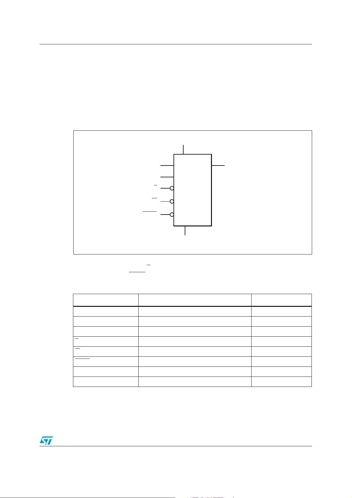
1 Description
The M95160 devices are Electrically Erasable PROgrammable Memories (EEPROMs)
organized as 2048 x 8 bits, accessed through the SPI bus.
The M95160 devices can operate with a supply range from 2.5 V up to 5.5 V, and are
guaranteed over the -40 °C/+125 °C temperature range. They are compliant with the
Automotive standard AEC-Q100 Grade 1.
Figure 1. Logic diagram
The SPI bus signals are C, D and Q, as shown in Figure 1 and Tab le 1 . The device is
selected when Chip Select (S
interrupted when the H
Table 1. Signal names
Signal name Function Direction
C Serial Clock Input
D Serial Data Input Input
Q Serial Data Output Output
S
W
Hold Input
HOLD
V
CC
V
SS
) is driven low. Communications with the device can be
OLD is driven low.
Chip Select Input
Write Protect Input
Supply voltage
Ground
Doc ID 022578 Rev 1 6/38

Description M95160-125
DV
SS
C
HOLDQ
SV
CC
W
AI01790D
M95xxx
1
2
3
4
8
7
6
5
Figure 2. 8-pin package connections (top view)
1. See Section 10: Package mechanical data section for package dimensions, and how to identify pin 1.
7/38 Doc ID 022578 Rev 1
M95160-125 Memory organization
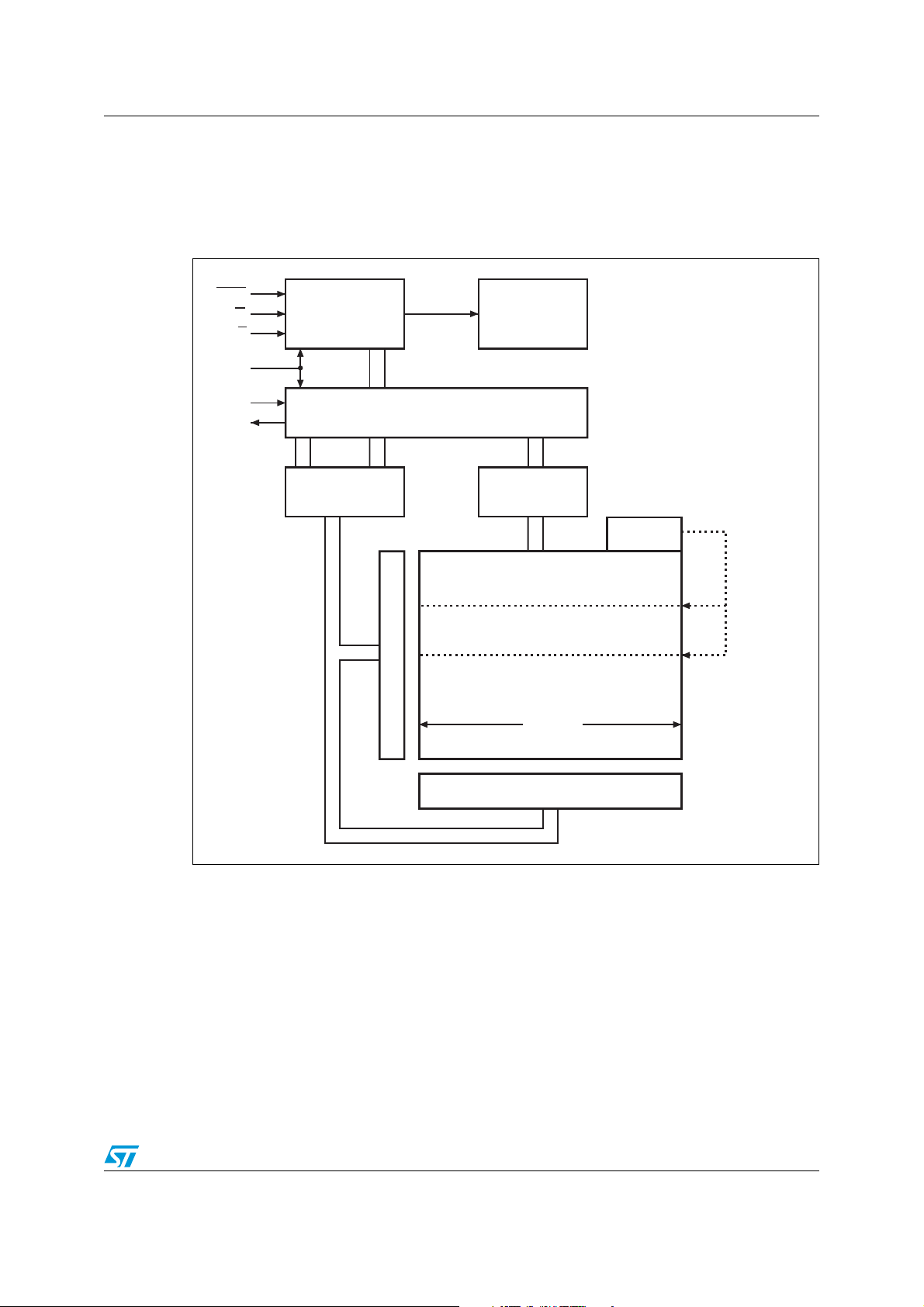
AI01272d
HOLD
S
W
Control logic
High voltage
generator
I/O shift register
Address register
and counter
Data
register
1 page
X decoder
Y decoder
C
D
Q
Size of the
read-only
EEPROM
area
Status
Register
2 Memory organization
The memory is organized as shown in the following figure.
Figure 3. Block diagram
Doc ID 022578 Rev 1 8/38

Signal description M95160-125
3 Signal description
During all operations, VCC must be held stable and within the specified valid range:
V
(min) to VCC(max).
CC
All of the input and output signals must be held high or low (according to voltages of V
V
, VIL or VOL, as specified in Section 9: DC and AC parameters). These signals are
OH
described next.
3.1 Serial Data Output (Q)
This output signal is used to transfer data serially out of the device. Data is shifted out on the
falling edge of Serial Clock (C).
3.2 Serial Data Input (D)
This input signal is used to transfer data serially into the device. It receives instructions,
addresses, and the data to be written. Values are latched on the rising edge of Serial Clock
(C).
,
IH
3.3 Serial Clock (C)
This input signal provides the timing of the serial interface. Instructions, addresses, or data
present at Serial Data Input (D) are latched on the rising edge of Serial Clock (C). Data on
Serial Data Output (Q) change from the falling edge of Serial Clock (C).
3.4 Chip Select (S)
When this input signal is high, the device is deselected and Serial Data Output (Q) is at high
impedance. The device is in the Standby Power mode, unless an internal Write cycle is in
progress. Driving Chip Select (S
After power-up, a falling edge on Chip Select (S
instruction.
3.5 Hold (HOLD)
The Hold (HOLD) signal is used to pause any serial communications with the device without
deselecting the device.
During the Hold condition, the Serial Data Output (Q) is high impedance, and Serial Data
Input (D) and Serial Clock (C) are Don’t Care.
To start the Hold condition, the device must be selected, with Chip Select (S
) low selects the device, placing it in the Active Power mode.
) is required prior to the start of any
) driven low.
9/38 Doc ID 022578 Rev 1

M95160-125 Signal description
3.6 Write Protect (W)
The main purpose of this input signal is to freeze the size of the area of memory that is
protected against Write instructions (as specified by the values in the BP1 and BP0 bits of
the Status Register).
This pin must be driven either high or low, and must be stable during all Write instructions.
3.7 V
supply voltage
CC
VCC is the supply voltage.
3.8 VSS ground
VSS is the reference for all signals, including the VCC supply voltage.
Doc ID 022578 Rev 1 10/38

Connecting to the SPI bus M95160-125
AI12836b
SPI Bus Master
SPI Memory
Device
SDO
SDI
SCK
CQD
S
SPI Memory
Device
CQD
S
SPI Memory
Device
CQD
S
CS3 CS2 CS1
SPI Interface with
(CPOL, CPHA) =
(0, 0) or (1, 1)
W
HOLD
W
HOLD
W
HOLD
RR R
V
CC
V
CC
V
CC
V
CC
V
SS
V
SS
V
SS
V
SS
R
4 Connecting to the SPI bus
All instructions, addresses and input data bytes are shifted in to the device, most significant
bit first. The Serial Data Input (D) is sampled on the first rising edge of the Serial Clock (C)
after Chip Select (S
All output data bytes are shifted out of the device, most significant bit first. The Serial Data
Output (Q) is latched on the first falling edge of the Serial Clock (C) after the instruction
(such as the Read from Memory Array and Read Status Register instructions) have been
clocked into the device.
Figure 4. Bus master and memory devices on the SPI bus
) goes low.
1. The Write Protect (W) and Hold (HOLD) signals should be driven, high or low as appropriate.
Figure 4 shows an example of three memory devices connected to an SPI bus master. Only
one memory device is selected at a time, so only one memory device drives the Serial Data
Output (Q) line at a time. The other memory devices are high impedance.
The pull-up resistor R (represented in Figure 4) ensures that a device is not selected if the
Bus Master leaves the S
line in the high impedance state.
In applications where the Bus Master may leave all SPI bus lines in high impedance at the
same time (for example, if the Bus Master is reset during the transmission of an instruction),
the clock line (C) must be connected to an external pull-down resistor so that, if all
inputs/outputs become high impedance, the C line is pulled low (while the S
11/38 Doc ID 022578 Rev 1
high): this ensures that S
t
requirement is met. The typical value of R is 100 kΩ..
SHCH
and C do not become high at the same time, and so, that the
line is pulled

M95160-125 Connecting to the SPI bus
AI01438B
C
MSB
CPHA
D
0
1
CPOL
0
1
Q
C
MSB
4.1 SPI modes
These devices can be driven by a microcontroller with its SPI peripheral running in either of
the following two modes:
● CPOL=0, CPHA=0
● CPOL=1, CPHA=1
For these two modes, input data is latched in on the rising edge of Serial Clock (C), and
output data is available from the falling edge of Serial Clock (C).
The difference between the two modes, as shown in Figure 5, is the clock polarity when the
bus master is in Stand-by mode and not transferring data:
● C remains at 0 for (CPOL=0, CPHA=0)
● C remains at 1 for (CPOL=1, CPHA=1)
Figure 5. SPI modes supported
Doc ID 022578 Rev 1 12/38
 Loading...