

Automotive 128-Kbit serial SPI bus EEPROMs
UFDFPN8 (MC)
2 x 3 mm
TSSOP8 (DW)
169 mil width
SO8 (MN)
150 mil width
Features
■ Compatible with the Serial Peripheral Interface
(SPI) bus
■ Memory array
– 128 Kbits ( Kbytes) of EEPROM
– Page size: 64 bytes
– Write protection by block: 1/4, 1/2 or whole
memory
– Additional Write lockable Page
(Identification page)
■ Extended temperature and voltage ranges
– Up to 125 °C: 1.8 V to 5.5 V
– Up to 145 °C: 2.5 V to 5.5 V
■ High speed clock frequency
–20MHz for V
–10MHz for V
–5MHz for V
■ Schmitt trigger inputs for noise filtering
■ Short Write cycle time
– Byte Write within 4 ms
– Page Write within 4 ms
■ Write cycle endurance
– 4 million Write cycles at 25 °C
– 1.2 million Write cycles at 85 °C
– 600 k Write cycles at 125 °C
– 400 k Write cycles at 145 °C
■ Data retention
– 40 years at 55 °C
– 100 years at 25 °C
■ ESD Protection (Human Body Model)
– 4000 V
■ Packages
– RoHS-compliant and halogen-free
(ECOPACK2
CC ≥
CC ≥
CC ≥
®
)
4.5 V
2.5 V
1.8 V
M95128-A125
M95128-A145
with high-speed clock
Datasheet − preliminary data
April 2012 Doc ID 023103 Rev 1 1/39
This is preliminary information on a new product now in development or undergoing evaluation. Details are subject to
change without notice.
www.st.com
1

Contents M95128-A125 M95128-A145
Contents
1 Description . . . . . . . . . . . . . . . . . . . . . . . . . . . . . . . . . . . . . . . . . . . . . . . . . 6
2 Signal description . . . . . . . . . . . . . . . . . . . . . . . . . . . . . . . . . . . . . . . . . . . 8
2.1 Serial Data output (Q) . . . . . . . . . . . . . . . . . . . . . . . . . . . . . . . . . . . . . . . . 8
2.2 Serial Data input (D) . . . . . . . . . . . . . . . . . . . . . . . . . . . . . . . . . . . . . . . . . . 8
2.3 Serial Clock (C) . . . . . . . . . . . . . . . . . . . . . . . . . . . . . . . . . . . . . . . . . . . . . 8
2.4 Chip Select (S
2.5 Hold (HOLD
2.6 Write Protect (W
2.7 V
2.8 V
ground . . . . . . . . . . . . . . . . . . . . . . . . . . . . . . . . . . . . . . . . . . . . . . . . . 8
SS
supply voltage . . . . . . . . . . . . . . . . . . . . . . . . . . . . . . . . . . . . . . . . . . . 8
CC
) . . . . . . . . . . . . . . . . . . . . . . . . . . . . . . . . . . . . . . . . . . . . . . 8
) . . . . . . . . . . . . . . . . . . . . . . . . . . . . . . . . . . . . . . . . . . . . . . . . 8
) . . . . . . . . . . . . . . . . . . . . . . . . . . . . . . . . . . . . . . . . . . . . 8
3 Operating features . . . . . . . . . . . . . . . . . . . . . . . . . . . . . . . . . . . . . . . . . . 9
3.1 Active power and Standby power modes . . . . . . . . . . . . . . . . . . . . . . . . . . 9
3.2 SPI modes . . . . . . . . . . . . . . . . . . . . . . . . . . . . . . . . . . . . . . . . . . . . . . . . . 9
3.3 Hold mode . . . . . . . . . . . . . . . . . . . . . . . . . . . . . . . . . . . . . . . . . . . . . . . . 10
3.4 Protocol control and data protection . . . . . . . . . . . . . . . . . . . . . . . . . . . . . 10
3.4.1 Protocol control . . . . . . . . . . . . . . . . . . . . . . . . . . . . . . . . . . . . . . . . . . . 10
3.4.2 Status Register and data protection . . . . . . . . . . . . . . . . . . . . . . . . . . . 11
3.5 Identification page . . . . . . . . . . . . . . . . . . . . . . . . . . . . . . . . . . . . . . . . . . 13
4 Instructions . . . . . . . . . . . . . . . . . . . . . . . . . . . . . . . . . . . . . . . . . . . . . . . 14
4.1 Write Enable (WREN) . . . . . . . . . . . . . . . . . . . . . . . . . . . . . . . . . . . . . . . 15
4.2 Write Disable (WRDI) . . . . . . . . . . . . . . . . . . . . . . . . . . . . . . . . . . . . . . . . 15
4.3 Read Status Register (RDSR) . . . . . . . . . . . . . . . . . . . . . . . . . . . . . . . . . 16
4.4 Write Status Register (WRSR) . . . . . . . . . . . . . . . . . . . . . . . . . . . . . . . . . 16
4.5 Read from Memory Array (READ) . . . . . . . . . . . . . . . . . . . . . . . . . . . . . . 17
4.6 Write to Memory Array (WRITE) . . . . . . . . . . . . . . . . . . . . . . . . . . . . . . . 18
4.7 Read Identification Page (RDID) . . . . . . . . . . . . . . . . . . . . . . . . . . . . . . . 20
4.8 Write Identification Page (WRID) . . . . . . . . . . . . . . . . . . . . . . . . . . . . . . . 21
4.9 Read Lock Status (RDLS) . . . . . . . . . . . . . . . . . . . . . . . . . . . . . . . . . . . . 21
4.10 Lock Identification Page (LID) . . . . . . . . . . . . . . . . . . . . . . . . . . . . . . . . . 22
2/39 Doc ID 023103 Rev 1

M95128-A125 M95128-A145 Contents
5 Application design recommendations . . . . . . . . . . . . . . . . . . . . . . . . . 24
5.1 Supply voltage (VCC) . . . . . . . . . . . . . . . . . . . . . . . . . . . . . . . . . . . . . . . . 24
5.1.1 Operating supply voltage V
5.1.2 Power-up conditions . . . . . . . . . . . . . . . . . . . . . . . . . . . . . . . . . . . . . . . 24
5.1.3 Power-down . . . . . . . . . . . . . . . . . . . . . . . . . . . . . . . . . . . . . . . . . . . . . . 25
CC . . . . . . . . . . . . . . . . . . . . . . . . . . . . . . . . . . . . . . . . . 24
5.2 Implementing devices on SPI bus . . . . . . . . . . . . . . . . . . . . . . . . . . . . . . 25
5.3 Cycling with Error Correction Code (ECC) . . . . . . . . . . . . . . . . . . . . . . . . 26
6 Delivery state . . . . . . . . . . . . . . . . . . . . . . . . . . . . . . . . . . . . . . . . . . . . . . 27
7 Absolute maximum ratings . . . . . . . . . . . . . . . . . . . . . . . . . . . . . . . . . . 27
8 DC and AC parameters . . . . . . . . . . . . . . . . . . . . . . . . . . . . . . . . . . . . . . 28
9 Package mechanical data . . . . . . . . . . . . . . . . . . . . . . . . . . . . . . . . . . . . 34
10 Part numbering . . . . . . . . . . . . . . . . . . . . . . . . . . . . . . . . . . . . . . . . . . . . 37
11 Revision history . . . . . . . . . . . . . . . . . . . . . . . . . . . . . . . . . . . . . . . . . . . 38
Doc ID 023103 Rev 1 3/39

List of tables M95128-A125 M95128-A145
List of tables
Table 1. Signal names . . . . . . . . . . . . . . . . . . . . . . . . . . . . . . . . . . . . . . . . . . . . . . . . . . . . . . . . . . . . 7
Table 2. Status Register format . . . . . . . . . . . . . . . . . . . . . . . . . . . . . . . . . . . . . . . . . . . . . . . . . . . . 11
Table 3. Write-protected block size . . . . . . . . . . . . . . . . . . . . . . . . . . . . . . . . . . . . . . . . . . . . . . . . . 12
Table 4. Protection modes . . . . . . . . . . . . . . . . . . . . . . . . . . . . . . . . . . . . . . . . . . . . . . . . . . . . . . . . 12
Table 5. Device identification bytes . . . . . . . . . . . . . . . . . . . . . . . . . . . . . . . . . . . . . . . . . . . . . . . . . 13
Table 6. Instruction set . . . . . . . . . . . . . . . . . . . . . . . . . . . . . . . . . . . . . . . . . . . . . . . . . . . . . . . . . . . 14
Table 7. Significant bits within the two address bytes . . . . . . . . . . . . . . . . . . . . . . . . . . . . . . . . . . . 14
Table 8. Absolute maximum ratings . . . . . . . . . . . . . . . . . . . . . . . . . . . . . . . . . . . . . . . . . . . . . . . . . 27
Table 9. Cycling performance by groups of 4 bytes . . . . . . . . . . . . . . . . . . . . . . . . . . . . . . . . . . . . . 28
Table 10. Operating conditions (voltage range W, temperature range 4) . . . . . . . . . . . . . . . . . . . . . . 28
Table 11. Operating conditions (voltage range R, temperature range 3) . . . . . . . . . . . . . . . . . . . . . . 28
Table 12. Operating conditions (voltage range R, temperature range 3)
for high speed communications . . . . . . . . . . . . . . . . . . . . . . . . . . . . . . . . . . . . . . . . . . . . . 28
Table 13. DC characteristics (voltage range W, temperature range 4). . . . . . . . . . . . . . . . . . . . . . . . 29
Table 14. DC characteristics (voltage range R, temperature range 3) . . . . . . . . . . . . . . . . . . . . . . . . 30
Table 15. AC characteristics . . . . . . . . . . . . . . . . . . . . . . . . . . . . . . . . . . . . . . . . . . . . . . . . . . . . . . . . 31
Table 16. SO8N – 8-lead plastic small outline, 150 mils body width, package mechanical data . . . . 34
Table 17. TSSOP8 – 8-lead thin shrink small outline, package mechanical data. . . . . . . . . . . . . . . . 35
Table 18. UFDFPN8 (MLP8) 8-lead ultra thin fine pitch dual flat package no lead
2 x 3 mm, data . . . . . . . . . . . . . . . . . . . . . . . . . . . . . . . . . . . . . . . . . . . . . . . . . . . . . . . . . . 36
Table 19. Ordering information scheme . . . . . . . . . . . . . . . . . . . . . . . . . . . . . . . . . . . . . . . . . . . . . . . 37
Table 20. Document revision history . . . . . . . . . . . . . . . . . . . . . . . . . . . . . . . . . . . . . . . . . . . . . . . . . 38
4/39 Doc ID 023103 Rev 1

M95128-A125 M95128-A145 List of figures
List of figures
Figure 1. Logic diagram . . . . . . . . . . . . . . . . . . . . . . . . . . . . . . . . . . . . . . . . . . . . . . . . . . . . . . . . . . . . 6
Figure 2. 8-pin package connections . . . . . . . . . . . . . . . . . . . . . . . . . . . . . . . . . . . . . . . . . . . . . . . . . . 7
Figure 3. SPI modes supported . . . . . . . . . . . . . . . . . . . . . . . . . . . . . . . . . . . . . . . . . . . . . . . . . . . . . . 9
Figure 4. Hold mode activation . . . . . . . . . . . . . . . . . . . . . . . . . . . . . . . . . . . . . . . . . . . . . . . . . . . . . 10
Figure 5. Write Enable (WREN) sequence . . . . . . . . . . . . . . . . . . . . . . . . . . . . . . . . . . . . . . . . . . . . 15
Figure 6. Write Disable (WRDI) sequence . . . . . . . . . . . . . . . . . . . . . . . . . . . . . . . . . . . . . . . . . . . . . 15
Figure 7. Read Status Register (RDSR) sequence . . . . . . . . . . . . . . . . . . . . . . . . . . . . . . . . . . . . . . 16
Figure 8. Write Status Register (WRSR) sequence. . . . . . . . . . . . . . . . . . . . . . . . . . . . . . . . . . . . . . 17
Figure 9. Read from Memory Array (READ) sequence . . . . . . . . . . . . . . . . . . . . . . . . . . . . . . . . . . . 18
Figure 10. Byte Write (WRITE) sequence . . . . . . . . . . . . . . . . . . . . . . . . . . . . . . . . . . . . . . . . . . . . . . 18
Figure 11. Page Write (WRITE) sequence . . . . . . . . . . . . . . . . . . . . . . . . . . . . . . . . . . . . . . . . . . . . . 19
Figure 12. Read Identification Page sequence . . . . . . . . . . . . . . . . . . . . . . . . . . . . . . . . . . . . . . . . . . 20
Figure 13. Write Identification Page sequence . . . . . . . . . . . . . . . . . . . . . . . . . . . . . . . . . . . . . . . . . . 21
Figure 14. Read Lock Status sequence . . . . . . . . . . . . . . . . . . . . . . . . . . . . . . . . . . . . . . . . . . . . . . . . 22
Figure 15. Lock ID sequence . . . . . . . . . . . . . . . . . . . . . . . . . . . . . . . . . . . . . . . . . . . . . . . . . . . . . . . . 22
Figure 16. Bus master and memory devices on the SPI bus . . . . . . . . . . . . . . . . . . . . . . . . . . . . . . . . 25
Figure 17. AC measurement I/O waveform . . . . . . . . . . . . . . . . . . . . . . . . . . . . . . . . . . . . . . . . . . . . . 32
Figure 18. Serial input timing . . . . . . . . . . . . . . . . . . . . . . . . . . . . . . . . . . . . . . . . . . . . . . . . . . . . . . . . 32
Figure 19. Hold timing . . . . . . . . . . . . . . . . . . . . . . . . . . . . . . . . . . . . . . . . . . . . . . . . . . . . . . . . . . . . . 32
Figure 20. Serial output timing . . . . . . . . . . . . . . . . . . . . . . . . . . . . . . . . . . . . . . . . . . . . . . . . . . . . . . . 33
Figure 21. SO8N – 8-lead plastic small outline, 150 mils body width, package outline . . . . . . . . . . . . 34
Figure 22. TSSOP8 – 8-lead thin shrink small outline, package outline . . . . . . . . . . . . . . . . . . . . . . . 35
Figure 23. UFDFPN8 (MLP8) - 8-lead ultra thin fine pitch dual flat no lead, package
outline . . . . . . . . . . . . . . . . . . . . . . . . . . . . . . . . . . . . . . . . . . . . . . . . . . . . . . . . . . . . . . . . . 36
Doc ID 023103 Rev 1 5/39
Description M95128-A125 M95128-A145
-36
(/,$
3
7
#ONTROLLOGIC
(IGHVOLTAGE
GENERATOR
)/SHIFTREGISTER
!DDRESSREGISTER
ANDCOUNTER
$ATA
REGISTER
PAGE
8DECODER
9DECODER
#
$
1
3IZEOFTHE
2EADONLY
%%02/AREA
3TATUS
REGISTER
)DENTIFICATIONPAGE
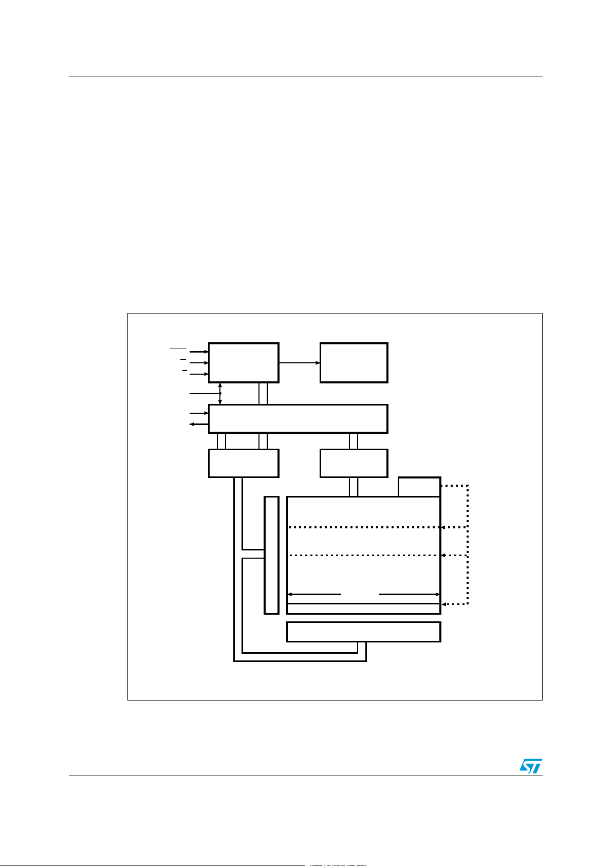
1 Description
The M95128-A125 and M95128-A145 are 128-Kbit serial EEPROM Automotive grade
devices operating up to 145°C. They are compliant with the very high level of reliability
defined by the Automotive standard AEC-Q100 grade 0.
The devices are accessed by a simple serial SPI compatible interface running up to 20 MHz.
The memory array is based on advanced true EEPROM technology (Electrically Erasable
PROgrammable Memory). The M95128-A125 and M95128-A145 are byte-alterable
memories (16384 × 8 bits) organized as 256 pages of 64 bytes in which the data integrity is
significantly improved with an embedded Error Correction Code logic.
The M95128-A125 and M95128-A145 offer an additional Identification Page (64 bytes) in
which the ST device identification can be read. This page can also be used to store sensitive
application parameters which can be later permanently locked in read-only mode.
Figure 1. Logic diagram
6/39 Doc ID 023103 Rev 1
M95128-A125 M95128-A145 Description
DV
SS
C
HOLDQ
SV
CC
W
AI01790D
M95xxx
1
2
3
4
8
7
6
5
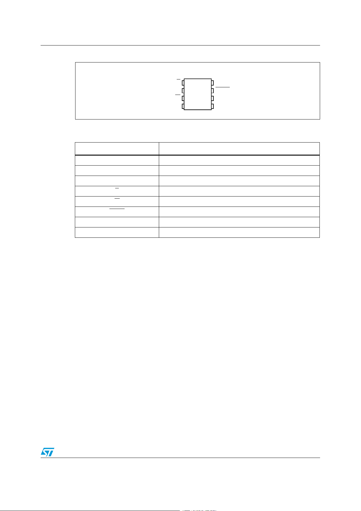
Figure 2. 8-pin package connections
1. See Package mechanical data section for package dimensions and how to identify pin-1.
Table 1. Signal names
Signal name Description
C Serial Clock
D Serial data input
Q Serial data output
S Chip Select
W
Write Protect
HOLD
V
CC
V
SS
Hold
Supply voltage
Ground
Doc ID 023103 Rev 1 7/39

Signal description M95128-A125 M95128-A145
2 Signal description
All input signals must be held high or low (according to voltages of VIH or VIL, as specified in
Ta bl e 1 3 and Ta bl e 1 4 )). These signals are described below.
2.1 Serial Data output (Q)
This output signal is used to transfer data serially out of the device during a Read operation.
Data is shifted out on the falling edge of Serial Clock (C), most significant bit (MSB) first. In
all other cases, the Serial Data output is in high impedance.
2.2 Serial Data input (D)
This input signal is used to transfer data serially into the device. D input receives
instructions, addresses, and the data to be written. Values are latched on the rising edge of
Serial Clock (C), most significant bit (MSB) first.
2.3 Serial Clock (C)
This input signal allows to synchronize the timing of the serial interface. Instructions,
addresses, or data present at Serial Data Input (D) are latched on the rising edge of Serial
Clock (C). Data on Serial Data Output (Q) changes after the falling edge of Serial Clock (C).
2.4 Chip Select (S)
Driving Chip Select (S) low selects the device in order to start communication. Driving Chip
Select (S
state.
) high deselects the device and Serial Data output (Q) enters the high impedance
2.5 Hold (HOLD)
The Hold (HOLD) signal is used to pause any serial communications with the device without
deselecting the device.
2.6 Write Protect (W)
This pin is used to write-protect the Status Register.
2.7 VSS ground
VSS is the reference for all signals, including the VCC supply voltage.
2.8 VCC supply voltage
VCC is the supply voltage pin.
Refer to Section 3.1: Active power and Standby power modes and to Section 5.1: Supply
voltage (VCC).
8/39 Doc ID 023103 Rev 1
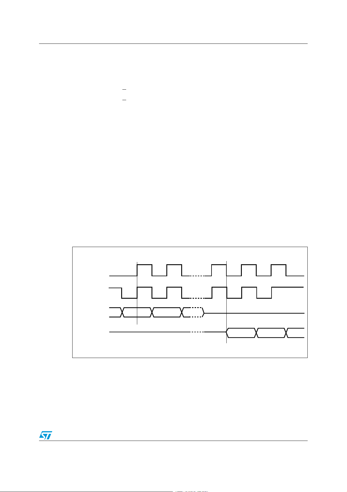
M95128-A125 M95128-A145 Operating features
AI01438B
C
MSB
CPHA
D
0
1
CPOL
0
1
Q
C
MSB
3 Operating features
3.1 Active power and Standby power modes
When Chip Select (S) is low, the device is selected and in the Active power mode.
When Chip Select (S
progress, the device then goes in to the Standby power mode, and the device consumption
drops to I
, as specified in Ta bl e 1 3 and Ta bl e 1 4 .
CC1
3.2 SPI modes
The device can be driven by a microcontroller with its SPI peripheral running in either of the
two following modes:
● CPOL=0, CPHA=0
● CPOL=1, CPHA=1
For these two modes, input data is latched in on the rising edge of Serial Clock (C), and
output data is available from the falling edge of Serial Clock (C).
The difference between the two modes, as shown in Figure 3, is the clock polarity when the
bus master is in Stand-by mode and not transferring data:
● C remains at 0 for (CPOL=0, CPHA=0)
● C remains at 1 for (CPOL=1, CPHA=1)
Figure 3. SPI modes supported
) is high, the device is deselected. If a Write cycle is not currently in
Doc ID 023103 Rev 1 9/39
Operating features M95128-A125 M95128-A145
(/,$
#
(OLD
CONDITION
#
N
(OLD
CONDITION
-36
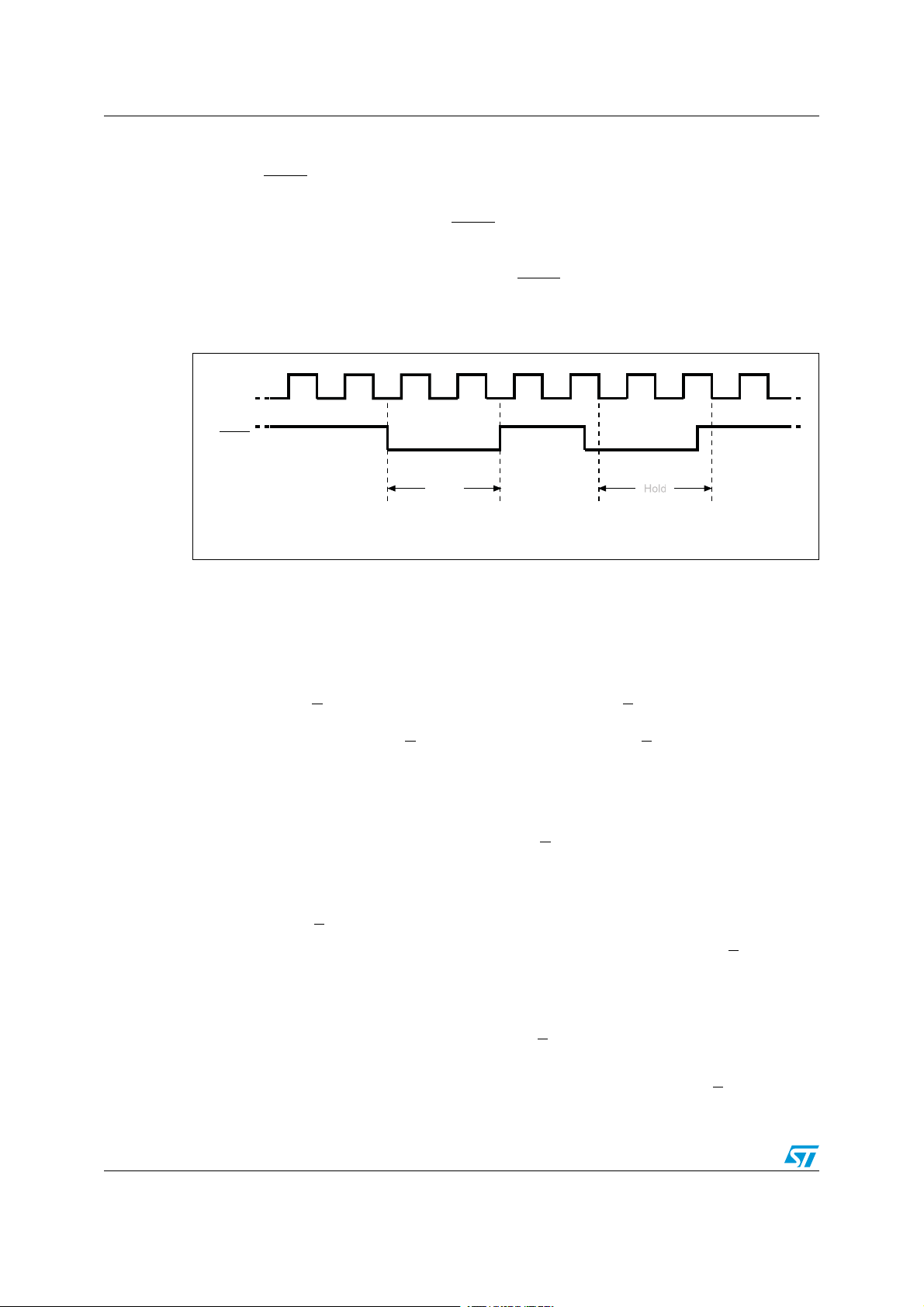
3.3 Hold mode
The Hold (HOLD) signal is used to pause any serial communications with the device without
resetting the clocking sequence.
The Hold mode starts when the Hold (HOLD
) signal is driven low and the Serial Clock (C) is
low (as shown in Figure 4). During the Hold mode, the Serial Data output (Q) is high
impedance, and the signals present on Serial Data input (D) and Serial Clock (C) are not
decoded. The Hold mode ends when the Hold (HOLD
Clock (C) is or becomes low.
Figure 4. Hold mode activation
Deselecting the device while it is in Hold mode resets the paused communication.
3.4 Protocol control and data protection
) signal is driven high and the Serial
ONDITIO
3.4.1 Protocol control
The Chip Select (S) input offers a built-in safety feature, as the S input is edge-sensitive as
well as level-sensitive: after power-up, the device is not selected until a falling edge has first
been detected on Chip Select (S
prior to going low, in order to start the first operation.
For Write commands (WRITE, WRSR, WRID, LID) to be accepted and executed:
● the Write Enable Latch (WEL) bit must be set by a Write Enable (WREN) instruction
● a falling edge and a low state on Chip Select (S) during the whole command must be
decoded
● instruction, address and input data must be sent as multiple of eight bits
● the command must include at least one data byte
● Chip Select (S) must be driven high exactly after a data byte boundary
Write command can be discarded at any time by a rising edge on Chip Select (S
a byte boundary.
To execute Read commands (READ, RDSR, RDID, RDLS), the device must decode:
● a falling edge and a low level on Chip Select (S) during the whole command
● instruction and address as multiples of eight bits (bytes)
From this step, data bits are shifted out until the rising edge on Chip Select (S
). This ensures that Chip Select (S) must have been high
) outside of
).
10/39 Doc ID 023103 Rev 1

M95128-A125 M95128-A145 Operating features
3.4.2 Status Register and data protection
The Status Register format is shown in Ta b le 2 and the status and control bits of the Status
Register are as follows:
Table 2. Status Register format
b7 b6 b5 b4 b3 b2 b1 b0
SRWD 0 0 0 BP1 BP0 WEL WIP
Status Register Write Protect
Block Protect bits
Write Enable Latch bit
Write In Progress bit
Note: Bits b6, b5, b4 are always read as 0.
WIP bit
The WIP bit (Write In Progress) is a read-only flag that indicates the Ready/Busy state of the
device. When a Write command (WRITE, WRSR, WRID, LID) has been decoded and a
Write cycle (t
the device is ready to decode a new command.
) is in progress, the device is busy and the WIP bit is set to 1. When WIP=0,
W
During a Write cycle, reading continuously the WIP bit allows to detect when the device
becomes ready (WIP=0) to decode a new command.
WEL bit
The WEL bit (Write Enable Latch) bit is a flag that indicates the status of the internal Write
Enable Latch. When WEL is set to 1, the Write instructions (WRITE, WRSR, WRID, LID) are
executed; when WEL is set to 0, any decoded Write instruction is not executed.
The WEL bit is set to 1 with the WREN instruction. The WEL bit is reset to 0 after the
following events:
● Write Disable (WRDI) instruction completion
● Write instructions (WRITE, WRSR, WRID, LID) completion including the write cycle
time t
W
Power-up
●
BP1, BP0 bits
The Block Protect bits (BP1, BP0) are non-volatile. BP1,BP0 bits define the size of the
memory block to be protected against write instructions, as defined in Ta bl e 2 . These bits
are written with the Write Status Register (WRSR) instruction, provided that the Status
Register is not protected (refer to SRWD bit and W input signal).
Doc ID 023103 Rev 1 11/39

Operating features M95128-A125 M95128-A145
Table 3. Write-protected block size
Status Register bits
Protected block Protected array addresses
BP1 BP0
0 0 None None
0 1 Upper quarter 3000h-3FFFh
1 0 Upper half 2000h-3FFFh
1 1 Whole memory 0000h - 3FFFh plus Identification page
SRWD bit and W input signal
The Status Register Write Disable (SRWD) bit is operated in conjunction with the Write
Protect pin (W
Register, regardless of whether the pin Write Protect (W
When the SRWD bit is written to 1, two cases have to be considered, depending on the
state of the W
● Case 1: if pin W is driven high, it is possible to write the Status Register.
● Case 2: if pin W is driven low, it is not possible to write the Status Register (WRSR is
discarded) and therefore SRWD,BP1,BP0 bits cannot be changed (the size of the
protected memory block defined by BP1,BP0 bits is frozen).
) signal. When the SRWD bit is written to 0, it is possible to write the Status
) is driven high or low.
input pin:
Case 2 can be entered in either sequence:
● Writing SRWD bit to 1 after driving pin W low, or
● Driving pin W low after writing SRWD bit to 1.
The only way to exit Case 2 is to pull pin W
Note: if pin W
is permanently tied high, the Status Register cannot be write-protected.
high.
The protection features of the device are summarized in Tab l e 4 .
Table 4. Protection modes
SRWD bit W signal Status
0X
11
1 0 Status Register is write-protected.
Status Register is writable.
12/39 Doc ID 023103 Rev 1
 Loading...