

Automotive 4-Kbit, 2-Kbit and 1-Kbit SPI bus EEPROM
SO8 (MN)
150 mil width
TSSOP8 (DW)
169 mil width
Features
■ Compatible with the Serial Peripheral Interface
(SPI) bus
■ Memory array
– 1 Kbit, 2 Kbit or 4 Kbit of EEPROM
– Page size: 16 bytes
– Write protection by block: 1/4, 1/2 or whole
memory
■ 5 MHz clock frequency
■ Write cycle within 5 ms
■ Operating temperature range: -40 °C to
+125 °C
■ Single supply voltage:
– 4.5 V to 5.5 V for M950x0
– 2.5 V to 5.5 V for M950x0-W
■ More than 1 million Write cycles
■ More than 40-year data retention
■ Enhanced ESD protection
■ Packages
– RoHS-compliant and halogen-free
(ECOPACK2
®
)
M95040-125
M95020-125 M95010-125
January 2012 Doc ID 022545 Rev 1 1/36
www.st.com
1

Contents M95040-125, M95020-125, M95010-125
Contents
1 Description . . . . . . . . . . . . . . . . . . . . . . . . . . . . . . . . . . . . . . . . . . . . . . . . . 6
2 Signal description . . . . . . . . . . . . . . . . . . . . . . . . . . . . . . . . . . . . . . . . . . . 8
2.1 Serial Data output (Q) . . . . . . . . . . . . . . . . . . . . . . . . . . . . . . . . . . . . . . . . 8
2.2 Serial Data input (D) . . . . . . . . . . . . . . . . . . . . . . . . . . . . . . . . . . . . . . . . . . 8
2.3 Serial Clock (C) . . . . . . . . . . . . . . . . . . . . . . . . . . . . . . . . . . . . . . . . . . . . . 8
2.4 Chip Select (S
2.5 Hold (HOLD
2.6 Write Protect (W
2.7 V
ground . . . . . . . . . . . . . . . . . . . . . . . . . . . . . . . . . . . . . . . . . . . . . . . . . 9
SS
2.8 Supply voltage (V
2.9 Supply voltage (V
2.9.1 Operating supply voltage V
2.9.2 Device reset . . . . . . . . . . . . . . . . . . . . . . . . . . . . . . . . . . . . . . . . . . . . . . . 9
2.9.3 Power-up conditions . . . . . . . . . . . . . . . . . . . . . . . . . . . . . . . . . . . . . . . 10
2.9.4 Power-down . . . . . . . . . . . . . . . . . . . . . . . . . . . . . . . . . . . . . . . . . . . . . . 10
) . . . . . . . . . . . . . . . . . . . . . . . . . . . . . . . . . . . . . . . . . . . . . . 8
) . . . . . . . . . . . . . . . . . . . . . . . . . . . . . . . . . . . . . . . . . . . . . . . . 8
) . . . . . . . . . . . . . . . . . . . . . . . . . . . . . . . . . . . . . . . . . . . . 9
) . . . . . . . . . . . . . . . . . . . . . . . . . . . . . . . . . . . . . . . . . 9
CC
) . . . . . . . . . . . . . . . . . . . . . . . . . . . . . . . . . . . . . . . . . 9
CC
CC . . . . . . . . . . . . . . . . . . . . . . . . . . . . . . . . . . . . . . . . . . 9
3 Connecting to the SPI bus . . . . . . . . . . . . . . . . . . . . . . . . . . . . . . . . . . . 11
3.1 SPI modes . . . . . . . . . . . . . . . . . . . . . . . . . . . . . . . . . . . . . . . . . . . . . . . . 12
4 Operating features . . . . . . . . . . . . . . . . . . . . . . . . . . . . . . . . . . . . . . . . . 13
4.1 Hold condition . . . . . . . . . . . . . . . . . . . . . . . . . . . . . . . . . . . . . . . . . . . . . . 13
4.2 Status register . . . . . . . . . . . . . . . . . . . . . . . . . . . . . . . . . . . . . . . . . . . . . 13
4.3 Data protection and protocol control . . . . . . . . . . . . . . . . . . . . . . . . . . . . 14
5 Memory organization . . . . . . . . . . . . . . . . . . . . . . . . . . . . . . . . . . . . . . . 15
6 Instructions . . . . . . . . . . . . . . . . . . . . . . . . . . . . . . . . . . . . . . . . . . . . . . . 16
6.1 Write Enable (WREN) . . . . . . . . . . . . . . . . . . . . . . . . . . . . . . . . . . . . . . . 16
6.2 Write Disable (WRDI) . . . . . . . . . . . . . . . . . . . . . . . . . . . . . . . . . . . . . . . . 17
6.3 Read Status Register (RDSR) . . . . . . . . . . . . . . . . . . . . . . . . . . . . . . . . . 18
6.3.1 WIP bit . . . . . . . . . . . . . . . . . . . . . . . . . . . . . . . . . . . . . . . . . . . . . . . . . . 18
6.3.2 WEL bit . . . . . . . . . . . . . . . . . . . . . . . . . . . . . . . . . . . . . . . . . . . . . . . . . 18
2/36 Doc ID 022545 Rev 1

M95040-125, M95020-125, M95010-125 Contents
6.3.3 BP1, BP0 bits . . . . . . . . . . . . . . . . . . . . . . . . . . . . . . . . . . . . . . . . . . . . . 18
6.4 Write Status Register (WRSR) . . . . . . . . . . . . . . . . . . . . . . . . . . . . . . . . . 20
6.5 Read from Memory Array (READ) . . . . . . . . . . . . . . . . . . . . . . . . . . . . . . 21
6.6 Write to Memory Array (WRITE) . . . . . . . . . . . . . . . . . . . . . . . . . . . . . . . 22
7 Power-up and delivery states . . . . . . . . . . . . . . . . . . . . . . . . . . . . . . . . . 24
7.1 Power-up state . . . . . . . . . . . . . . . . . . . . . . . . . . . . . . . . . . . . . . . . . . . . . 24
7.2 Initial delivery state . . . . . . . . . . . . . . . . . . . . . . . . . . . . . . . . . . . . . . . . . . 24
8 Maximum rating . . . . . . . . . . . . . . . . . . . . . . . . . . . . . . . . . . . . . . . . . . . . 25
9 DC and AC parameters . . . . . . . . . . . . . . . . . . . . . . . . . . . . . . . . . . . . . . 26
10 Package mechanical data . . . . . . . . . . . . . . . . . . . . . . . . . . . . . . . . . . . . 32
11 Part numbering . . . . . . . . . . . . . . . . . . . . . . . . . . . . . . . . . . . . . . . . . . . . 34
12 Revision history . . . . . . . . . . . . . . . . . . . . . . . . . . . . . . . . . . . . . . . . . . . 35
Doc ID 022545 Rev 1 3/36

List of tables M95040-125, M95020-125, M95010-125
List of tables
Table 1. Signal names . . . . . . . . . . . . . . . . . . . . . . . . . . . . . . . . . . . . . . . . . . . . . . . . . . . . . . . . . . . . 7
Table 2. Write-protected block size . . . . . . . . . . . . . . . . . . . . . . . . . . . . . . . . . . . . . . . . . . . . . . . . . 14
Table 3. Instruction set . . . . . . . . . . . . . . . . . . . . . . . . . . . . . . . . . . . . . . . . . . . . . . . . . . . . . . . . . . . 16
Table 4. Status register format . . . . . . . . . . . . . . . . . . . . . . . . . . . . . . . . . . . . . . . . . . . . . . . . . . . . . 18
Table 5. Address range bits . . . . . . . . . . . . . . . . . . . . . . . . . . . . . . . . . . . . . . . . . . . . . . . . . . . . . . . 21
Table 6. Absolute maximum ratings . . . . . . . . . . . . . . . . . . . . . . . . . . . . . . . . . . . . . . . . . . . . . . . . . 25
Table 7. Operating conditions (M950x0, device grade 3) . . . . . . . . . . . . . . . . . . . . . . . . . . . . . . . . . 26
Table 8. Operating conditions (M950x0-W, device grade 3) . . . . . . . . . . . . . . . . . . . . . . . . . . . . . . 26
Table 9. AC test measurement conditions . . . . . . . . . . . . . . . . . . . . . . . . . . . . . . . . . . . . . . . . . . . . 26
Table 10. Capacitance . . . . . . . . . . . . . . . . . . . . . . . . . . . . . . . . . . . . . . . . . . . . . . . . . . . . . . . . . . . . 27
Table 11. DC characteristics (M950x0, device grade 3) . . . . . . . . . . . . . . . . . . . . . . . . . . . . . . . . . . . 27
Table 12. DC characteristics (M950x0-W, device grade 3) . . . . . . . . . . . . . . . . . . . . . . . . . . . . . . . . 27
Table 13. AC characteristics (M950x0, device grade 3) . . . . . . . . . . . . . . . . . . . . . . . . . . . . . . . . . . . 28
Table 14. AC characteristics (M950x0-W, device grade 3). . . . . . . . . . . . . . . . . . . . . . . . . . . . . . . . . 29
Table 15. SO8N — 8-lead plastic small outline, 150 mils body width, package
mechanical data . . . . . . . . . . . . . . . . . . . . . . . . . . . . . . . . . . . . . . . . . . . . . . . . . . . . . . . . . 32
Table 16. TSSOP8 — 8-lead thin shrink small outline, package mechanical data . . . . . . . . . . . . . . . 33
Table 17. Ordering information scheme . . . . . . . . . . . . . . . . . . . . . . . . . . . . . . . . . . . . . . . . . . . . . . . 34
Table 18. Document revision history . . . . . . . . . . . . . . . . . . . . . . . . . . . . . . . . . . . . . . . . . . . . . . . . . 35
4/36 Doc ID 022545 Rev 1

M95040-125, M95020-125, M95010-125 List of figures
List of figures
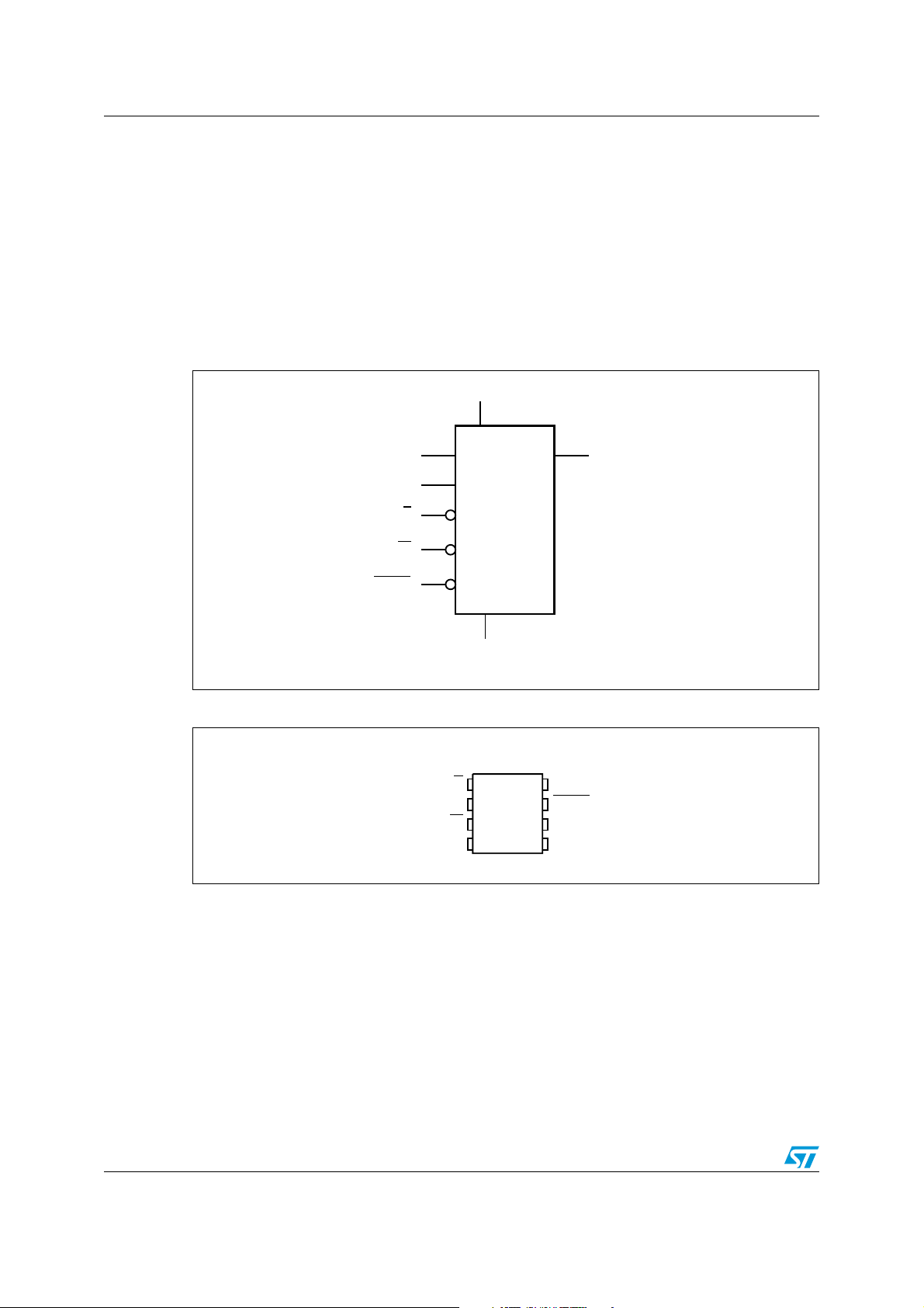
Figure 1. Logic diagram . . . . . . . . . . . . . . . . . . . . . . . . . . . . . . . . . . . . . . . . . . . . . . . . . . . . . . . . . . . . 6
Figure 2. 8-pin package connections . . . . . . . . . . . . . . . . . . . . . . . . . . . . . . . . . . . . . . . . . . . . . . . . . . 6
Figure 3. Bus master and memory devices on the SPI bus . . . . . . . . . . . . . . . . . . . . . . . . . . . . . . . . 11
Figure 4. SPI modes supported . . . . . . . . . . . . . . . . . . . . . . . . . . . . . . . . . . . . . . . . . . . . . . . . . . . . . 12
Figure 5. Hold condition activation . . . . . . . . . . . . . . . . . . . . . . . . . . . . . . . . . . . . . . . . . . . . . . . . . . . 13
Figure 6. Block diagram . . . . . . . . . . . . . . . . . . . . . . . . . . . . . . . . . . . . . . . . . . . . . . . . . . . . . . . . . . . 15
Figure 7. Write Enable (WREN) sequence . . . . . . . . . . . . . . . . . . . . . . . . . . . . . . . . . . . . . . . . . . . . 16
Figure 8. Write Disable (WRDI) sequence . . . . . . . . . . . . . . . . . . . . . . . . . . . . . . . . . . . . . . . . . . . . . 17
Figure 9. Read Status Register (RDSR) sequence . . . . . . . . . . . . . . . . . . . . . . . . . . . . . . . . . . . . . . 19
Figure 10. Write Status Register (WRSR) sequence . . . . . . . . . . . . . . . . . . . . . . . . . . . . . . . . . . . . . . 20
Figure 11. Read from Memory Array (READ) sequence . . . . . . . . . . . . . . . . . . . . . . . . . . . . . . . . . . . 21
Figure 12. Byte Write (WRITE) sequence . . . . . . . . . . . . . . . . . . . . . . . . . . . . . . . . . . . . . . . . . . . . . . 22
Figure 13. Page Write (WRITE) sequence . . . . . . . . . . . . . . . . . . . . . . . . . . . . . . . . . . . . . . . . . . . . . 23
Figure 14. AC test measurement I/O waveform. . . . . . . . . . . . . . . . . . . . . . . . . . . . . . . . . . . . . . . . . . 26
Figure 15. Serial input timing . . . . . . . . . . . . . . . . . . . . . . . . . . . . . . . . . . . . . . . . . . . . . . . . . . . . . . . . 30
Figure 16. Hold timing . . . . . . . . . . . . . . . . . . . . . . . . . . . . . . . . . . . . . . . . . . . . . . . . . . . . . . . . . . . . . 30
Figure 17. Serial output timing . . . . . . . . . . . . . . . . . . . . . . . . . . . . . . . . . . . . . . . . . . . . . . . . . . . . . . . 31
Figure 18. SO8N — 8-lead plastic small outline 150 mils body width, package outline. . . . . . . . . . . . 32
Figure 19. TSSOP8 — 8-lead thin shrink small outline, package outline. . . . . . . . . . . . . . . . . . . . . . . 33
Doc ID 022545 Rev 1 5/36
Description M95040-125, M95020-125, M95010-125
AI01789C
S
V
CC
M95xxx
HOLD
V
SS
W
Q
C
D
DV
SS
C
HOLDQ
SV
CC
W
AI01790D
M95xxx
1
2
3
4
8
7
6
5
1 Description
The M950x0-125 devices are 1-Kbit, 2-Kbit and 4-Kbit Electrically Erasable PROgrammable
Memories (EEPROM) accessed through the SPI bus, synchronized with a clock running up
to 5 MHz.
The devices can operate with supply voltages ranging from 2.5 V to 5.5 V.
The devices are guaranteed over the -40°C/+125°C temperature range and are compliant
with the Automotive standard AEC-Q100 Grade 1.
Figure 1. Logic diagram
Figure 2. 8-pin package connections
1. See Section 10: Package mechanical data for package dimensions, and how to identify pin 1.
6/36 Doc ID 022545 Rev 1
M95040-125, M95020-125, M95010-125 Description
Table 1. Signal names
Signal name Function
C Serial Clock
D Serial Data input
Q Serial Data output
S Chip Select
Write Protect
W
Hold
HOLD
V
CC
V
SS
Supply voltage
Ground
Doc ID 022545 Rev 1 7/36

Signal description M95040-125, M95020-125, M95010-125
2 Signal description
During all operations, VCC must be held stable and within the specified valid range:
V
(min) to VCC(max).
CC
All of the input and output signals can be held high or low (according to voltages of V
V
or VOL, as specified in Section 9: DC and AC parameters). These signals are described
IL
next.
2.1 Serial Data output (Q)
This output signal is used to transfer data serially out of the device. Data is shifted out on the
falling edge of Serial Clock (C).
2.2 Serial Data input (D)
This input signal is used to transfer data serially into the device. It receives instructions,
addresses, and the data to be written. Values are latched on the rising edge of Serial Clock
(C).
, VOH,
IH
2.3 Serial Clock (C)
This input signal provides the timing of the serial interface. Instructions, addresses, or data
present at Serial Data Input (D) are latched on the rising edge of Serial Clock (C). Data on
Serial Data Output (Q) changes after the falling edge of Serial Clock (C).
2.4 Chip Select (S)
When this input signal is high, the device is deselected and Serial Data Output (Q) is at high
impedance. Unless an internal Write cycle is in progress, the device will be in the Standby
Power mode. Driving Chip Select (S
mode.
After Power-up, a falling edge on Chip Select (S
instruction.
2.5 Hold (HOLD)
The Hold (HOLD) signal is used to pause any serial communications with the device without
deselecting the device.
During the Hold condition, the Serial Data Output (Q) is high impedance, and Serial Data
Input (D) and Serial Clock (C) are Don’t Care.
To start the Hold condition, the device must be selected, with Chip Select (S
) low selects the device, placing it in the Active Power
) is required prior to the start of any
) driven low.
8/36 Doc ID 022545 Rev 1

M95040-125, M95020-125, M95010-125 Signal description
2.6 Write Protect (W)
This input signal is used to control whether the memory is write protected. When Write
Protect (W
enabled. Write Protect (W
) is held low, writes to the memory are disabled, but other operations remain
) must either be driven high or low, but must not be left floating.
2.7 VSS ground
VSS is the reference for the VCC supply voltage.
2.8 Supply voltage (VCC)
2.9 Supply voltage (V
CC
)
2.9.1 Operating supply voltage V
Prior to selecting the memory and issuing instructions to it, a valid and stable VCC voltage
within the specified [V
(min), VCC(max)] range must be applied (see operating condition
CC
tables in Section 9: DC and AC parameters). This voltage must remain stable and valid until
the end of the transmission of the instruction and, for a Write instruction, until the completion
of the internal write cycle (t
recommended to decouple the V
nF to 100 nF) close to the V
). In order to secure a stable DC supply voltage, it is
W
CC
CC/VSS
2.9.2 Device reset
In order to prevent inadvertent write operations during power-up, a power-on-reset (POR)
circuit is included. At power-up, the device does not respond to any instruction until V
reaches the internal reset threshold voltage (this threshold is defined in operating condition
tables in Section 9: DC and AC parameters) as V
When V
● in Standby Power mode
● deselected (note that, to be executed, an instruction must be preceded by a falling
● Status register value:
passes over the POR threshold, the device is reset and is in the following state:
CC
edge on Chip Select (S
))
– the Write Enable Latch (WEL) is reset to 0
– Write In Progress (WIP) is reset to 0
– The SRWD, BP1 and BP0 bits remain unchanged (non-volatile bits)
CC
line with a suitable capacitor (usually of the order of 10
package pins.
CC
).
RES
When V
passes over the POR threshold, the device is reset and enters the Standby
CC
Power mode. The device must not be accessed until V
voltage within the specified [V
(min), VCC(max)] range defined in operating condition
CC
tables in Section 9: DC and AC parameters.
Doc ID 022545 Rev 1 9/36
reaches a valid and stable VCC
CC

Signal description M95040-125, M95020-125, M95010-125
2.9.3 Power-up conditions
When the power supply is turned on, VCC rises continuously from VSS to VCC. During this
time, the Chip Select (S
therefore recommended to connect the S
Figure 3).
) line is not allowed to float but should follow the VCC voltage. It is
line to VCC via a suitable pull-up resistor (see
In addition, the Chip Select (S
sensitive as well as level sensitive: after power-up, the device does not become selected
until a falling edge has first been detected on Chip Select (S
(S
) must have been high, prior to going low to start the first operation.
The V
voltage has to rise continuously from 0 V up to the minimum VCC operating voltage
CC
defined in operating condition tables in Section 9: DC and AC parameters and the rise time
must not vary faster than 1 V/µs.
2.9.4 Power-down
During power-down (continuous decrease in the VCC supply voltage below the minimum
V
operating voltage defined in operating condition tables in Section 9: DC and AC
CC
parameters), the device must be:
● deselected (Chip Select S should be allowed to follow the voltage applied on V
● in Standby Power mode (there should not be any internal write cycle in progress).
) input offers a built-in safety feature, as the S input is edge
). This ensures that Chip Select
)
CC
10/36 Doc ID 022545 Rev 1
M95040-125, M95020-125, M95010-125 Connecting to the SPI bus
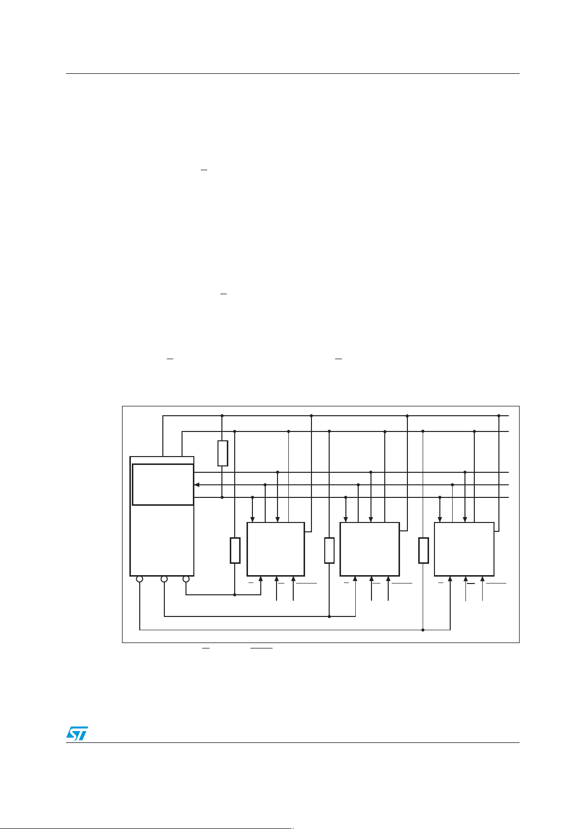
AI12304b
Bus master
SPI memory
device
SDO
SDI
SCK
CQD
S
SPI memory
device
CQD
S
SPI mmory
device
CQD
S
CS3 CS2 CS1
SPI Interface with
(CPOL, CPHA) =
(0, 0) or (1, 1)
W
HOLD
W
HOLD
W
HOLD
RRR
V
CC
V
CC
V
CC
V
CC
V
SS
V
SS
V
SS
V
SS
R
3 Connecting to the SPI bus
These devices are fully compatible with the SPI protocol.
All instructions, addresses and input data bytes are shifted in to the device, most significant
bit first. The Serial Data Input (D) is sampled on the first rising edge of the Serial Clock (C)
after Chip Select (S
All output data bytes are shifted out of the device, most significant bit first. The Serial Data
Output (Q) is latched on the first falling edge of the Serial Clock (C) after the instruction
(such as the Read from Memory Array and Read Status Register instructions) have been
clocked into the device.
Figure 3 shows an example of three memory devices connected to an MCU, on an SPI bus.
Only one memory device is selected at a time, so only one memory device drives the Serial
Data output (Q) line at a time, the other memory devices are high impedance.
The pull-up resistor R (represented in Figure 3) ensures that a device is not selected if the
bus master leaves the S
In applications where the bus master might enter a state where all SPI bus inputs/outputs
would be in high impedance at the same time (for example, if the bus master is reset during
the transmission of an Instruction), the clock line (C) must be connected to an external pull-
down resistor so that, if all inputs/outputs become high impedance, the C line is pulled low
(while the S
line is pulled high): this ensures that S and C do not become high at the same
time, and so, that the t
) goes low.
line in the high impedance state.
requirement is met. The typical value of R is 100 kΩ.
SHCH
Figure 3. Bus master and memory devices on the SPI bus
1. The Write Protect (W) and Hold (HOLD) signals should be driven high or low as appropriate.
Doc ID 022545 Rev 1 11/36
Connecting to the SPI bus M95040-125, M95020-125, M95010-125
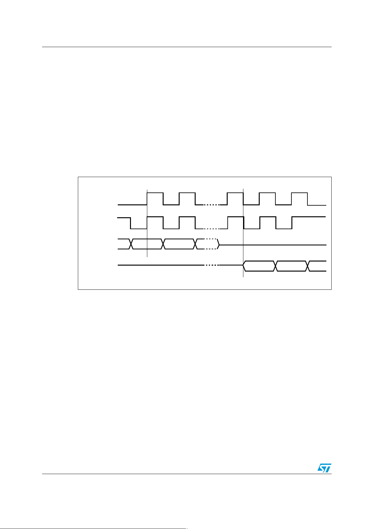
AI01438B
C
MSB
CPHA
D
0
1
CPOL
0
1
Q
C
MSB
3.1 SPI modes
These devices can be driven by a microcontroller with its SPI peripheral running in either of
the two following modes:
● CPOL=0, CPHA=0
● CPOL=1, CPHA=1
For these two modes, input data is latched in on the rising edge of Serial Clock (C), and
output data is available from the falling edge of Serial Clock (C).
The difference between the two modes, as shown in Figure 4, is the clock polarity when the
bus master is in Stand-by mode and not transferring data:
● C remains at 0 for (CPOL=0, CPHA=0)
● C remains at 1 for (CPOL=1, CPHA=1)
Figure 4. SPI modes supported
12/36 Doc ID 022545 Rev 1

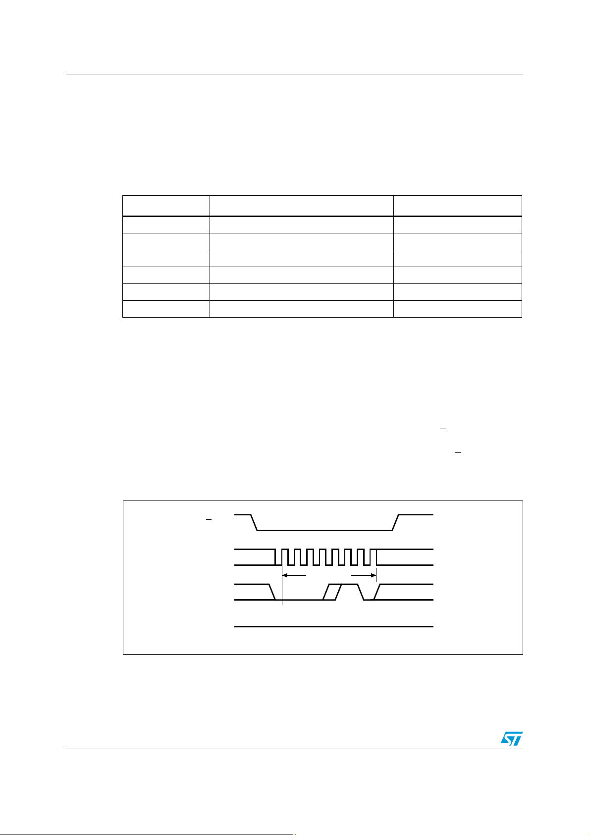
M95040-125, M95020-125, M95010-125 Operating features
AI02029D
HOLD
C
Hold
Condition
Hold
Condition
4 Operating features
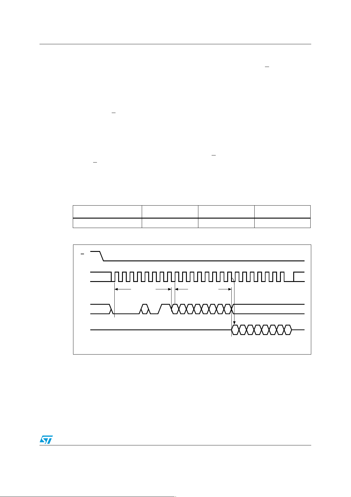
4.1 Hold condition
The Hold (HOLD) signal is used to pause any serial communications with the device without
resetting the clocking sequence.
During the Hold condition, the Serial Data Output (Q) is high impedance, and Serial Data
Input (D) and Serial Clock (C) are Don’t Care.
To enter the Hold condition, the device must be selected, with Chip Select (S
) low.
Normally, the device is kept selected, for the whole duration of the Hold condition.
Deselecting the device while it is in the Hold condition, has the effect of resetting the state of
the device, and this mechanism can be used if it is required to reset any processes that had
been in progress.
The Hold condition starts when the Hold (HOLD
) signal is driven low at the same time as
Serial Clock (C) already being low (as shown in Figure 5).
The Hold condition ends when the Hold (HOLD
) signal is driven high at the same time as
Serial Clock (C) already being low.
Figure 5 also shows what happens if the rising and falling edges are not timed to coincide
with Serial Clock (C) being low.
Figure 5. Hold condition activation
4.2 Status register
Figure 6 shows the position of the Status register in the control logic of the device. This
register contains a number of control bits and status bits, as shown in Table 4: Status
register format. For a detailed description of the Status register bits, see Section 6.3: Read
Status Register (RDSR).
Doc ID 022545 Rev 1 13/36
Operating features M95040-125, M95020-125, M95010-125
4.3 Data protection and protocol control
To help protect the device from data corruption in noisy or poorly controlled environments, a
number of safety features have been built in to the device. The main security measures can
be summarized as follows:
● The WEL bit is reset at power-up.
● Chip Select (S) must rise after the eighth clock count (or multiple thereof) in order to
start a non-volatile Write cycle (in the memory array or in the Status register).
● Accesses to the memory array are ignored during the non-volatile programming cycle,
and the programming cycle continues unaffected.
● Invalid Chip Select (S) and Hold (HOLD) transitions are ignored.
For any instruction to be accepted and executed, Chip Select (S
) must be driven high after
the rising edge of Serial Clock (C) that latches the last bit of the instruction, and before the
next rising edge of Serial Clock (C).
For this, “the last bit of the instruction” can be the eighth bit of the instruction code, or the
eighth bit of a data byte, depending on the instruction (except in the case of RDSR and
READ instructions). Moreover, the “next rising edge of CLOCK” might (or might not) be the
next bus transaction for some other device on the bus.
When a Write cycle is in progress, the device protects it against external interruption by
ignoring any subsequent READ, WRITE or WRSR instruction until the present cycle is
complete.
Table 2. Write-protected block size
Status register bits
Protected block
BP1 BP0 M95040 M95020 M95010
0 0 none none none none
0 1 Upper quarter 180h - 1FFh C0h - FFh 60h - 7Fh
1 0 Upper half 100h - 1FFh 80h - FFh 40h - 7Fh
1 1 Whole memory 000h - 1FFh 00h - FFh 00h - 7Fh
Protected array addresses
14/36 Doc ID 022545 Rev 1

M95040-125, M95020-125, M95010-125 Memory organization
AI01272d
HOLD
S
W
Control logic
High voltage
generator
I/O shift register
Address register
and counter
Data
register
1 page
X decoder
Y decoder
C
D
Q
Size of the
read-only
EEPROM
area
Status
Register
5 Memory organization
The memory is organized as shown in Figure 6.
Figure 6. Block diagram
Doc ID 022545 Rev 1 15/36
Instructions M95040-125, M95020-125, M95010-125
C
D
AI01441D
S
Q
21 34567
High Impedance
0
Instruction
6 Instructions
Each instruction starts with a single-byte code, as summarized in Ta b le 3 .
If an invalid instruction is sent (one not contained in Ta bl e 3 ), the device automatically
deselects itself.
Table 3. Instruction set
Instruction Description Instruction Format
WREN Write Enable 0000 X110
WRDI Write Disable 0000 X100
RDSR Read Status Register 0000 X101
WRSR Write Status Register 0000 X001
READ Read from Memory Array 0000 A8011
WRITE Write to Memory Array 0000 A8010
1. X = Don’t Care.
2. A8 = 1 for the upper half of the memory array of the M95040-125, and 0 for the lower half, and is Don’t
Care for other devices.
(1)
(1)
(1)
(1)
(2)
(2)
6.1 Write Enable (WREN)
The Write Enable Latch (WEL) bit must be set prior to each WRITE and WRSR instruction.
The only way to do this is to send a Write Enable instruction to the device.
As shown in Figure 7, to send this instruction to the device, Chip Select (S
and the bits of the instruction byte are shifted in, on Serial Data Input (D). The device then
enters a wait state. It waits for a the device to be deselected, by Chip Select (S
high.
Figure 7. Write Enable (WREN) sequence
) is driven low,
) being driven
16/36 Doc ID 022545 Rev 1
M95040-125, M95020-125, M95010-125 Instructions
C
D
AI03790D
S
Q
21 34567
High Impedance
0
Instruction
6.2 Write Disable (WRDI)
One way of resetting the Write Enable Latch (WEL) bit is to send a Write Disable instruction
to the device.
As shown in Figure 8, to send this instruction to the device, Chip Select (S
) is driven low,
and the bits of the instruction byte are shifted in, on Serial Data Input (D).
The device then enters a wait state. It waits for a the device to be deselected, by Chip Select
(S
) being driven high.
The Write Enable Latch (WEL) bit, in fact, becomes reset by any of the following events:
● Power-up
● WRDI instruction execution
● WRSR instruction completion
● WRITE instruction completion
● Write Protect (W) line being held low.
Figure 8. Write Disable (WRDI) sequence
Doc ID 022545 Rev 1 17/36

Instructions M95040-125, M95020-125, M95010-125
6.3 Read Status Register (RDSR)
One of the major uses of this instruction is to allow the MCU to poll the state of the Write In
Progress (WIP) bit. This is needed because the device will not accept further WRITE or
WRSR instructions when the previous Write cycle is not yet finished.
As shown in Figure 8, to send this instruction to the device, Chip Select (S
) is first driven low.
The bits of the instruction byte are then shifted in, on Serial Data Input (D). The current state
of the bits in the Status register is shifted out, on Serial Data Out (Q). The Read Cycle is
terminated by driving Chip Select (S
) high.
The Status register may be read at any time, even during a Write cycle (whether it be to the
memory area or to the Status register). All bits of the Status register remain valid, and can
be read using the RDSR instruction. However, during the current Write cycle, the values of
the non-volatile bits (BP0, BP1) become frozen at a constant value. The updated value of
these bits becomes available when a new RDSR instruction is executed, after completion of
the Write cycle. On the other hand, the two read-only bits (Write Enable Latch (WEL), Write
In Progress (WIP)) are dynamically updated during the ongoing Write cycle.
Bits b7, b6, b5 and b4 are always read as 1. The status and control bits of the Status
register are as follows:
Table 4. Status register format
b7 b0
1 1 1 1 BP1 BP0 WEL WIP
Block Protect bits
Write Enable Latch bit
Write In Progress bit
6.3.1 WIP bit
The Write In Progress (WIP) bit indicates whether the memory is busy with a Write or Write
Status register cycle. When set to 1, such a cycle is in progress, when reset to 0 no such
cycle is in progress.
6.3.2 WEL bit
The Write Enable Latch (WEL) bit indicates the status of the internal Write Enable Latch.
When set to 1 the internal Write Enable Latch is set, when set to 0 the internal Write Enable
Latch is reset and no Write or Write Status Register instruction is accepted.
6.3.3 BP1, BP0 bits
The Block Protect (BP1, BP0) bits are non-volatile. They define the size of the area to be
software protected against Write instructions. These bits are written with the Write Status
Register (WRSR) instruction. When one or both of the Block Protect (BP1, BP0) bits is set to
1, the relevant memory area (as defined in Table 2: Write-protected block size) becomes
protected against Write (WRITE) instructions. The Block Protect (BP1, BP0) bits can be
written provided that the Hardware Protected mode has not been set.
18/36 Doc ID 022545 Rev 1

M95040-125, M95020-125, M95010-125 Instructions
C
D
S
21 3456789101112131415
Instruction
0
AI01444D
Q
7 6543210
Status Register Out
High Impedance
MSB
7 6543210
Status Register Out
MSB
7
Figure 9. Read Status Register (RDSR) sequence
Doc ID 022545 Rev 1 19/36

Instructions M95040-125, M95020-125, M95010-125
C
D
AI01445B
S
Q
21 3456789101112131415
High Impedance
Instruction Status
Register In
0
765432 0
1
MSB
6.4 Write Status Register (WRSR)
The Write Status Register (WRSR) instruction allows new values to be written to the Status
register. Before it can be accepted, a Write Enable (WREN) instruction must previously have
been executed.
The Write Status Register (WRSR) instruction is entered by driving Chip Select (S
) low,
sending the instruction code followed by the data byte on Serial Data input (D), and driving
the Chip Select (S
) signal high. Chip Select (S) must be driven high after the rising edge of
Serial Clock (C) that latches in the eighth bit of the data byte, and before the next rising edge
of Serial Clock (C). Otherwise, the Write Status Register (WRSR) instruction is not
executed.
Driving the Chip Select (S
timed write cycle that takes t
) signal high at a byte boundary of the input data triggers the self-
to complete (as specified in AC tables under Section 9: DC
W
and AC parameters). The instruction sequence is shown in Figure 10.
While the Write Status Register cycle is in progress, the Status register may still be read to
check the value of the Write in progress (WIP) bit: the WIP bit is 1 during the self-timed write
cycle t
reset at the end of the write cycle t
, and, 0 when the write cycle is complete. The WEL bit (Write enable latch) is also
W
.
W
The Write Status Register (WRSR) instruction allows the user to change the values of the
BP1, BP0 bits which define the size of the area that is to be treated as read only, as defined
in Table 2: Write-protected block size.
The contents of the BP1, BP0 bits are updated after the completion of the WRSR
instruction, including the t
write cycle.
W
The Write Status Register (WRSR) instruction has no effect on the b7, b6, b5, b4, b1 and b0
bits in the Status register. Bits b7, b6, b5, b4 are always read as 0.
Figure 10. Write Status Register (WRSR) sequence
The instruction is not accepted, and is not executed, under the following conditions:
● if the Write Enable Latch (WEL) bit has not been set to 1 (by executing a Write Enable
instruction just before)
● if a write cycle is already in progress
● if the device has not been deselected, by Chip Select (S) being driven high, after the
20/36 Doc ID 022545 Rev 1
eighth bit, b0, of the data byte has been latched in
● if Write Protect (W) is low during the WRSR command (instruction, address and data)
M95040-125, M95020-125, M95010-125 Instructions
C
D
AI01440E
S
Q
A7
21 345678910111213141516171819
A6 A5 A4 A3 A2 A1 A0A8
20 21 22
76543
2
0
1
High Impedance
Data Out
Instruction Byte Address
0
6.5 Read from Memory Array (READ)
As shown in Figure 11, to send this instruction to the device, Chip Select (S) is first driven
low. The bits of the instruction byte and address byte are then shifted in, on Serial Data Input
(D). For the M95040, the most significant address bit, A8, is incorporated as bit b3 of the
instruction byte, as shown in Table 3: Instruction set. The address is loaded into an internal
address register, and the byte of data at that address is shifted out, on Serial Data Output
(Q).
If Chip Select (S
) continues to be driven low, an internal bit-pointer is automatically
incremented at each clock cycle, and the corresponding data bit is shifted out.
When the highest address is reached, the address counter rolls over to zero, allowing the
Read cycle to be continued indefinitely. The whole memory can, therefore, be read with a
single READ instruction.
The Read cycle is terminated by driving Chip Select (S
Select (S
) signal can occur at any time during the cycle.
) high. The rising edge of the Chip
The first byte addressed can be any byte within any page.
The instruction is not accepted, and is not executed, if a Write cycle is currently in progress.
Table 5. Address range bits
Device M95040-125 M95020-125 M95010-125
Address bits A8-A0 A7-A0 A6-A0
Figure 11. Read from Memory Array (READ) sequence
1. Depending on the memory size, as shown in Table 5: Address range bits, the most significant address bits
are Don’t Care.
Doc ID 022545 Rev 1 21/36

Instructions M95040-125, M95020-125, M95010-125
AI01442D
C
D
S
Q
A7
21 345678910111213141516171819
A6 A5 A4 A3 A2 A1 A0A8
20 21 22 23
High Impedance
Instruction Byte Address
0
765432 0
1
Data Byte
6.6 Write to Memory Array (WRITE)
As shown in Figure 12, to send this instruction to the device, Chip Select (S) is first driven
low. The bits of the instruction byte, address byte, and at least one data byte are then shifted
in, on Serial Data input (D). The instruction is terminated by driving Chip Select (S
byte boundary of the input data. The self-timed Write cycle, triggered by the rising edge of
Chip Select (S
), continues for a period tW (as specified in tables under Section 9: DC and
AC parameters). After this time, the Write in Progress (WIP) bit is reset to 0.
) high at a
In the case of Figure 12, Chip Select (S
has been latched in, indicating that the instruction is being used to write a single byte. If,
though, Chip Select (S
) continues to be driven low, as shown in Figure 13, the next byte of
input data is shifted in, so that more than a single byte, starting from the given address
towards the end of the same page, can be written in a single internal Write cycle. If Chip
Select (S
) still continues to be driven low, the next byte of input data is shifted in, and used to
overwrite the byte at the start of the current page.
The instruction is not accepted, and is not executed, under the following conditions:
● if the Write Enable Latch (WEL) bit has not been set to 1 (by executing a Write Enable
instruction just before)
● if a Write cycle is already in progress
● if the device has not been deselected, by Chip Select (S) being driven high, at a byte
boundary (after the rising edge of Serial Clock (C) that latches the last data bit, and
before the next rising edge of Serial Clock (C) occurs anywhere on the bus)
● if Write Protect (W) is low or if the addressed page is in the area protected by the Block
Protect (BP1 and BP0) bits
Note: The self-timed write cycle t
events: [Erase addressed byte(s)], followed by [Program addressed byte(s)]. An erased bit is
read as “0” and a programmed bit is read as “1”.
Figure 12. Byte Write (WRITE) sequence
) is driven high after the eighth bit of the data byte
is internally executed as a sequence of two consecutive
W
1. Depending on the memory size, as shown in Table 5: Address range bits, the most significant address bits
are Don’t Care.
22/36 Doc ID 022545 Rev 1

M95040-125, M95020-125, M95010-125 Instructions
C
D
S
21 34567891011121314151617181920 21 22 23
Instruction Byte Address
0
Data Byte 1
C
D
AI01443D
S
2625 27 28 29 30 31
8+8N
24
Data Byte 16
9+8N
10+8N
11+8N
12+8N
13+8N
14+8N
15+8N
136
137
138
139
140
141
142
143
Data Byte N
76 3210
54
Data Byte 2
7
A7 A6 A5 A4 A3 A2 A1 A0A8 765432 0
1
7 6543210765432 0
1
Figure 13. Page Write (WRITE) sequence
1. Depending on the memory size, as shown in Table 5: Address range bits, the most significant address bits
are Don’t Care.
Doc ID 022545 Rev 1 23/36

Power-up and delivery states M95040-125, M95020-125, M95010-125
7 Power-up and delivery states
7.1 Power-up state
After power-up, the device is in the following state:
● low power Standby Power mode
● deselected (after Power-up, a falling edge is required on Chip Select (S) before any
instructions can be started).
● not in the Hold Condition
● the Write Enable Latch (WEL) is reset to 0
● Write In Progress (WIP) is reset to 0
The BP1 and BP0 bits of the Status register are unchanged from the previous power-down
(they are non-volatile bits).
7.2 Initial delivery state
The device is delivered with the memory array set at all 1s (FFh). The Block Protect (BP1
and BP0) bits are initialized to 0.
24/36 Doc ID 022545 Rev 1
M95040-125, M95020-125, M95010-125 Maximum rating
8 Maximum rating
Stressing the device outside the ratings listed in Ta bl e 6 may cause permanent damage to
the device. These are stress ratings only, and operation of the device at these, or any other
conditions outside those indicated in the operating sections of this specification, is not
implied. Exposure to absolute maximum rating conditions for extended periods may affect
device reliability.
Table 6. Absolute maximum ratings
Symbol Parameter Min. Max. Unit
Ambient operating temperature –40 130 °C
T
STG
T
LEAD
V
O
V
I
I
OL
I
IH
V
CC
V
ESD
1. Compliant with JEDEC Std J-STD-020 (for small body, Sn-Pb or Pb assembly), with the ST ECOPACK®
7191395 specification, and with the European directive on Restrictions on Hazardous Substances (RoHS)
2002/95/EU.
2. Positive and negative pulses applied on pin pairs, according to the AEC-Q100-002 (compliant with JEDEC
Std JESD22-A114, C1=100pF, R1=1500Ω, R2=500Ω)
Storage temperature –65 150 °C
Lead temperature during soldering see note
(1)
°C
Output voltage –0.50 VCC+0.6 V
Input voltage –0.50 6.5 V
DC output current (Q = 0) - 5 mA
DC output current (Q = 1) - 5 mA
Supply voltage –0.50 6.5 V
Electrostatic pulse (Human Body Model) voltage
(2)
- 4000 V
Doc ID 022545 Rev 1 25/36

DC and AC parameters M95040-125, M95020-125, M95010-125
!)#
6
##
6
##
6
##
6
##
)NPUTANDOUTPUT
TIMINGREFERENCELEVELS
)NPUTVOLTAGELEVELS
9 DC and AC parameters
This section summarizes the operating and measurement conditions, and the DC and AC
characteristics of the device. The parameters in the DC and AC characteristic tables that
follow are derived from tests performed under the measurement conditions summarized in
the relevant tables. Designers should check that the operating conditions in their circuit
match the measurement conditions when relying on the quoted parameters.
Table 7. Operating conditions (M950x0, device grade 3)
Symbol Parameter Min. Max. Unit
V
T
Table 8. Operating conditions (M950x0-W, device grade 3)
Supply voltage 4.5 5.5 V
CC
Ambient operating temperature –40 125 °C
A
Symbol Parameter Min. Max. Unit
V
T
Table 9. AC test measurement conditions
Supply voltage 2.5 5.5 V
CC
Ambient operating temperature –40 125 °C
A
Symbol Parameter Min. Max. Unit
C
Load capacitance 30 pF
L
Input rise and fall times - 50 ns
Input pulse voltages 0.2 VCC to 0.8 V
Input and output timing reference voltages 0.3 V
to 0.7 V
CC
CC
CC
Figure 14. AC test measurement I/O waveform
V
V
26/36 Doc ID 022545 Rev 1

M95040-125, M95020-125, M95010-125 DC and AC parameters
Table 10. Capacitance
Symbol Parameter Test condition
(1)
Min. Max. Unit
C
OUT
C
1. Sampled only, not 100% tested, at TA=25°C and a frequency of 5 MHz.
Table 11. DC characteristics (M950x0, device grade 3)
Output capacitance (Q) V
Input capacitance (D) VIN = 0 V - 8 pF
IN
Input capacitance (other pins) V
= 0 V - 8 pF
OUT
= 0 V - 6 pF
IN
Symbol Parameter Test condition Min. Max. Unit
Input leakage current V
I
LI
I
Output leakage current S = VCC, V
LO
I
I
V
V
V
V
RES
1. Characterized only, not tested in production.
Supply current
CC
Supply current
CC1
(Standby Power mode)
Input low voltage –0.45 0.3 V
V
IL
Input high voltage 0.7 V
IH
Output low voltage IOL = 2 mA, VCC = 5 V - 0.4 V
OL
Output high voltage IOH = –2 mA, VCC = 5V 0.8V
OH
Internal reset threshold
(1)
voltage
C = 0.1V
S = VCC, V
= VSS or V
IN
OUT
/0.9VCC at 5 MHz,
CC
CC
= VSS or V
VCC= 5 V, Q = open
= VSS or V
IN
V
= 5 V
CC
CC
CC
-± 2µA
-± 2µA
-3mA
-5µA
CC
CCVCC
CC
+1 V
-V
2.5 4.0 V
V
Table 12. DC characteristics (M950x0-W, device grade 3)
Symbol Parameter Test condition Min. Max. Unit
I
Input leakage current V
LI
Output leakage current S = VCC, V
I
LO
I
Supply current
CC
I
V
V
V
RES
1. Characterized only, not tested in production.
Supply current
CC1
(Standby Power mode)
V
Input low voltage –0.45 0.3 V
IL
Input high voltage 0.7 V
V
IH
Output low voltage IOL = 1.5 mA, VCC = 2.5 V - 0.4 V
OL
Output high voltage IOH = –0.4 mA, VCC = 2.5V 0.8V
OH
(1)
Internal reset threshold voltage 1.0 1.65 V
C = 0.1V
S = VCC, V
= VSS or V
IN
OUT
/0.9VCC at 5 MHz,
CC
= 2.5 V, Q = open
V
CC
IN
V
= 2.5 V
CC
CC
= VSS or V
= VSS or V
CC
CC
-± 2µA
-± 2µA
-2mA
-2µA
CC
CCVCC
CC
+1 V
-V
Doc ID 022545 Rev 1 27/36
V
DC and AC parameters M95040-125, M95020-125, M95010-125
Table 13. AC characteristics (M950x0, device grade 3)
Test conditions specified in Tab l e 9 and Table 7
Symbol Alt. Parameter Min. Max. Unit
f
C
t
SLCH
t
SHCH
t
SHSL
t
CHSH
t
CHSL
(1)
t
CH
(1)
t
CL
t
CLCH
t
CHCL
t
DVC H
t
CHDX
t
HHCH
t
HLCH
t
CLHL
t
CLHH
t
SHQZ
t
CLQV
t
CLQX
t
QLQH
t
QHQL
t
HHQV
t
HLQZ
t
W
1. tCH + tCL must never be less than the shortest possible clock period, 1 / fC(max)
2. Characterized only, not tested in production.
(2)
(2)
(2)
(2)
(2)
(2)
f
SCK
t
CSS1
t
CSS2
t
CS
t
CSH
t
CLH
t
CLL
t
RC
t
FC
t
DSU
t
DH
t
DIS
t
t
HO
t
RO
t
FO
t
LZ
t
HZ
t
WC
Clock frequency D.C. 5 MHz
S active setup time 90 - ns
S not active setup time 90 - ns
S deselect time 100 - ns
S active hold time 90 - ns
S not active hold time 90 - ns
Clock high time 90 - ns
Clock low time 90 - ns
Clock rise time 1 µs
Clock fall time 1 µs
Data in setup time 20 - ns
Data in hold time 30 - ns
Clock low hold time after HOLD not active 70 - ns
Clock low hold time after HOLD active 40 - ns
Clock low setup time before HOLD active 0 - ns
Clock low setup time before HOLD not active 0 - ns
Output disable time - 100 ns
Clock low to output valid - 60 ns
V
Output hold time 0 - ns
Output rise time - 50 ns
Output fall time - 50 ns
HOLD high to output valid - 50 ns
HOLD low to output high-Z - 100 ns
Write time - 5 ms
28/36 Doc ID 022545 Rev 1

M95040-125, M95020-125, M95010-125 DC and AC parameters
Table 14. AC characteristics (M950x0-W, device grade 3)
Test conditions specified in Tab l e 9 and Table 8
Symbol Alt. Parameter Min. Max. Unit
f
C
t
SLCH
t
SHCH
t
SHSL
t
CHSH
t
CHSL
(1)
t
CH
(1)
t
CL
t
CLCH
t
CHCL
t
DVC H
t
CHDX
t
HHCH
t
HLCH
t
CLHL
t
CLHH
t
SHQZ
t
CLQV
t
CLQX
t
QLQH
t
QHQL
t
HHQV
t
HLQZ
t
W
1. tCH + tCL must never be less than the shortest possible clock period, 1 / fC(max)
2. Characterized only, not tested in production.
(2)
(2)
(2)
(2)
(2)
(2)
f
SCK
t
CSS1
t
CSS2
t
CS
t
CSH
t
CLH
t
CLL
t
RC
t
FC
t
DSU
t
DH
t
DIS
t
t
HO
t
RO
t
FO
t
LZ
t
HZ
t
WC
Clock frequency D.C. 5 MHz
S active setup time 90 - ns
S not active setup time 90 - ns
S deselect time 100 - ns
S active hold time 90 - ns
S not active hold time 90 - ns
Clock high time 90 - ns
Clock low time 90 - ns
Clock rise time - 1 µs
Clock fall time - 1 µs
Data in setup time 20 - ns
Data in hold time 30 - ns
Clock low hold time after HOLD not active 70 - ns
Clock low hold time after HOLD active 40 - ns
Clock low setup time before HOLD active 0 - ns
Clock low setup time before HOLD not active 0 - ns
Output disable time - 100 ns
Clock low to output valid - 60 ns
V
Output hold time 0 - ns
Output rise time - 50 ns
Output fall time - 50 ns
HOLD high to output valid - 50 ns
HOLD low to output high-Z - 100 ns
Write time - 5 ms
Doc ID 022545 Rev 1 29/36

DC and AC parameters M95040-125, M95020-125, M95010-125
C
D
AI01447d
S
MSB IN
Q
tDVCH
High impedance
LSB IN
tSLCH
tCHDX
tCLCH
tSHCH
tSHSL
tCHSHtCHSL
tCH
tCL
tCHCL
C
Q
AI01448c
S
HOLD
tCLHL
tHLCH
tHHCH
tCLHH
tHHQVtHLQZ
Figure 15. Serial input timing
Figure 16. Hold timing
30/36 Doc ID 022545 Rev 1

M95040-125, M95020-125, M95010-125 DC and AC parameters
Figure 17. Serial output timing
S
C
tCLQX
Q
D
tCLQV
ADDR
LSB IN
tCLCH
tCHCL
tCH
tCL
tQLQH
tQHQL
tSHSL
tSHQZ
AI01449f
Doc ID 022545 Rev 1 31/36

Package mechanical data M95040-125, M95020-125, M95010-125
SO-A
E1
8
ccc
b
e
A
D
c
1
E
h x 45˚
A2
k
0.25 mm
L
L1
A1
GAUGE PLANE
10 Package mechanical data
In order to meet environmental requirements, ST offers these devices in different grades of
ECOPACK
specifications, grade definitions and product status are available at: www.st.com.
ECOPACK
®
packages, depending on their level of environmental compliance. ECOPACK®
®
is an ST trademark.
Figure 18. SO8N — 8-lead plastic small outline 150 mils body width, package outline
1. Drawing is not to scale.
Table 15. SO8N — 8-lead plastic small outline, 150 mils body width, package
mechanical data
millimeters inches
Symbol
Typ Min Max Typ Min Max
(1)
A - - 1.75 - - 0.0689
A1 - 0.1 0.25 - 0.0039 0.0098
A2 - 1.25 - - 0.0492 -
b - 0.28 0.48 - 0.011 0.0189
c - 0.17 0.23 - 0.0067 0.0091
ccc - - 0.1 - - 0.0039
D 4.9 4.8 5 0.1929 0.189 0.1969
E 6 5.8 6.2 0.2362 0.2283 0.2441
E1 3.9 3.8 4 0.1535 0.1496 0.1575
e 1.27 - - 0.05 - -
h - 0.25 0.5 - 0.0098 0.0197
k-0°8°-0°8°
L - 0.4 1.27 - 0.0157 0.05
32/36 Doc ID 022545 Rev 1
L1 1.04 - - 0.0409 - -
1. Values in inches are converted from mm and rounded to 4 decimal digits.
M95040-125, M95020-125, M95010-125 Package mechanical data
TSSOP8AM
1
8
CP
c
L
EE1
D
A2A
α
eb
4
5
A1
L1
Figure 19. TSSOP8 — 8-lead thin shrink small outline, package outline
1. Drawing is not to scale.
Table 16. TSSOP8 — 8-lead thin shrink small outline, package mechanical data
millimeters inches
Symbol
Typ Min Max Typ Min Max
(1)
A - - 1.2 - - 0.0472
A1 - 0.05 0.15 - 0.002 0.0059
A2 1 0.8 1.05 0.0394 0.0315 0.0413
b - 0.19 0.3 - 0.0075 0.0118
c - 0.09 0.2 - 0.0035 0.0079
CP - - 0.1 - - 0.0039
D 3 2.9 3.1 0.1181 0.1142 0.122
e0.65--0.0256--
E 6.4 6.2 6.6 0.252 0.2441 0.2598
E1 4.4 4.3 4.5 0.1732 0.1693 0.1772
L 0.6 0.45 0.75 0.0236 0.0177 0.0295
L1 1 - - 0.0394 - -
α - 0° 8° - 0° 8°
N (number of leads) 8 8
1. Values in inches are converted from mm and rounded to 4 decimal digits.
Doc ID 022545 Rev 1 33/36

Part numbering M95040-125, M95020-125, M95010-125
11 Part numbering
Table 17. Ordering information scheme
Example: M95040 – W MN 3 T P /S
Device type
M95 = SPI serial access EEPROM
Device function
040 = 4 Kbit (512 x 8)
020 = 2 Kbit (256 x 8)
010 = 1 Kbit (128 x 8)
Operating voltage
blank = V
W = VCC = 2.5 to 5.5V
Package
MN = SO8 (150 mil width)
DW = TSSOP8 (169 mil width)
= 4.5 to 5.5V
CC
Device grade
3 = Device tested with high reliability certified flow.
Automotive temperature range (–40 to 125 °C)
Option
blank = Standard packing
T = Tape and reel packing
Plating technology
P = RoHS compliant and halogen-free (ECOPACK
Process
/S = Manufacturing technology code
®
)
For a list of available options (speed, package, etc.) or for further information on any aspect
of this device, please contact your nearest ST sales office.
34/36 Doc ID 022545 Rev 1

M95040-125, M95020-125, M95010-125 Revision history
12 Revision history
Table 18. Document revision history
Date Version Changes
02-Jan-2012 1 Initial release.
Doc ID 022545 Rev 1 35/36

M95040-125, M95020-125, M95010-125
Please Read Carefully:
Information in this document is provided solely in connection with ST products. STMicroelectronics NV and its subsidiaries (“ST”) reserve the
right to make changes, corrections, modifications or improvements, to this document, and the products and services described herein at any
time, without notice.
All ST products are sold pursuant to ST’s terms and conditions of sale.
Purchasers are solely responsible for the choice, selection and use of the ST products and services described herein, and ST assumes no
liability whatsoever relating to the choice, selection or use of the ST products and services described herein.
No license, express or implied, by estoppel or otherwise, to any intellectual property rights is granted under this document. If any part of this
document refers to any third party products or services it shall not be deemed a license grant by ST for the use of such third party products
or services, or any intellectual property contained therein or considered as a warranty covering the use in any manner whatsoever of such
third party products or services or any intellectual property contained therein.
UNLESS OTHERWISE SET FORTH IN ST’S TERMS AND CONDITIONS OF SALE ST DISCLAIMS ANY EXPRESS OR IMPLIED
WARRANTY WITH RESPECT TO THE USE AND/OR SALE OF ST PRODUCTS INCLUDING WITHOUT LIMITATION IMPLIED
WARRANTIES OF MERCHANTABILITY, FITNESS FOR A PARTICULAR PURPOSE (AND THEIR EQUIVALENTS UNDER THE LAWS
OF ANY JURISDICTION), OR INFRINGEMENT OF ANY PATENT, COPYRIGHT OR OTHER INTELLECTUAL PROPERTY RIGHT.
UNLESS EXPRESSLY APPROVED IN WRITING BY TWO AUTHORIZED ST REPRESENTATIVES, ST PRODUCTS ARE NOT
RECOMMENDED, AUTHORIZED OR WARRANTED FOR USE IN MILITARY, AIR CRAFT, SPACE, LIFE SAVING, OR LIFE SUSTAINING
APPLICATIONS, NOR IN PRODUCTS OR SYSTEMS WHERE FAILURE OR MALFUNCTION MAY RESULT IN PERSONAL INJURY,
DEATH, OR SEVERE PROPERTY OR ENVIRONMENTAL DAMAGE. ST PRODUCTS WHICH ARE NOT SPECIFIED AS "AUTOMOTIVE
GRADE" MAY ONLY BE USED IN AUTOMOTIVE APPLICATIONS AT USER’S OWN RISK.
Resale of ST products with provisions different from the statements and/or technical features set forth in this document shall immediately void
any warranty granted by ST for the ST product or service described herein and shall not create or extend in any manner whatsoever, any
liability of ST.
ST and the ST logo are trademarks or registered trademarks of ST in various countries.
Information in this document supersedes and replaces all information previously supplied.
The ST logo is a registered trademark of STMicroelectronics. All other names are the property of their respective owners.
© 2012 STMicroelectronics - All rights reserved
STMicroelectronics group of companies
Australia - Belgium - Brazil - Canada - China - Czech Republic - Finland - France - Germany - Hong Kong - India - Israel - Italy - Japan -
Malaysia - Malta - Morocco - Philippines - Singapore - Spain - Sweden - Switzerland - United Kingdom - United States of America
www.st.com
36/36 Doc ID 022545 Rev 1
 Loading...