


4Kbit, 2Kbit and 1Kbit Serial SPI Bus EEPROM
FEAT URES SUM MAR Y
■ Compatible with SPI Bus Serial Interface
(Positive Clock SPI Modes)
■ Single Supply Voltage:
– 4.5 to 5.5V for M950x0
– 2.5 to 5.5V for M950x0-W
– 1.8 to 5.5V for M950x0-R
■ High Speed
– 10MHz Clock Rate, 5ms Write Time
■ Status Register
■ BYTE and PAGE WRITE (up to 16 Bytes)
■ Self-Timed Programming Cycle
■ Adjustable Size Read-Only EEPROM Area
■ Enhanced ESD Protection
■ More than 1 Million Erase/Write Cycles
■ More than 40-Year Data Retention
M95040
M95020, M95010
With High Speed Clock
Figure 1. Packages
8
1
PDIP8 (BN)
8
Table 1. Product List
Reference Part Number
M95040
M95020
M95010
M95040
M95040-W
M95040-R
M95020
M95020-W
M95020-R
M95010
M95010-W
M95010-R
1
SO8 (MN)
150 mil width
TSSOP8 (DW)
169 mil width
1/37October 2004

M95040, M95020, M95010
TABLE OF CONTENTS
FEATURES SUMMARY . . . . . . . . . . . . . . . . . . . . . . . . . . . . . . . . . . . . . . . . . . . . . . . . . . . . . . . . . . . . . 1
Table 1. Product List . . . . . . . . . . . . . . . . . . . . . . . . . . . . . . . . . . . . . . . . . . . . . . . . . . . . . . . . . . . . 1
Figure 1. Packages. . . . . . . . . . . . . . . . . . . . . . . . . . . . . . . . . . . . . . . . . . . . . . . . . . . . . . . . . . . . . . 1
SUMMARY DESCRIPTION. . . . . . . . . . . . . . . . . . . . . . . . . . . . . . . . . . . . . . . . . . . . . . . . . . . . . . . . . . . 5
Figure 2. Logic Diagram . . . . . . . . . . . . . . . . . . . . . . . . . . . . . . . . . . . . . . . . . . . . . . . . . . . . . . . . . . 5
Figure 3. DIP, SO and TSSOP Connections . . . . . . . . . . . . . . . . . . . . . . . . . . . . . . . . . . . . . . . . . . 5
Table 2. Signal Names . . . . . . . . . . . . . . . . . . . . . . . . . . . . . . . . . . . . . . . . . . . . . . . . . . . . . . . . . . 5
SIGNAL DESCRIPTION . . . . . . . . . . . . . . . . . . . . . . . . . . . . . . . . . . . . . . . . . . . . . . . . . . . . . . . . . . . . . 6
Serial Data Output (Q). . . . . . . . . . . . . . . . . . . . . . . . . . . . . . . . . . . . . . . . . . . . . . . . . . . . . . . . . . . . 6
Serial Data Input (D) . . . . . . . . . . . . . . . . . . . . . . . . . . . . . . . . . . . . . . . . . . . . . . . . . . . . . . . . . . . . . 6
Serial Clock (C) . . . . . . . . . . . . . . . . . . . . . . . . . . . . . . . . . . . . . . . . . . . . . . . . . . . . . . . . . . . . . . . . .6
Chip Select (S) . . . . . . . . . . . . . . . . . . . . . . . . . . . . . . . . . . . . . . . . . . . . . . . . . . . . . . . . . . . . . . . . . 6
Hold (HOLD) . . . . . . . . . . . . . . . . . . . . . . . . . . . . . . . . . . . . . . . . . . . . . . . . . . . . . . . . . . . . . . . . . . . 6
Write Protect (W). . . . . . . . . . . . . . . . . . . . . . . . . . . . . . . . . . . . . . . . . . . . . . . . . . . . . . . . . . . . . . . . 6
CONNECTING TO THE SPI BUS . . . . . . . . . . . . . . . . . . . . . . . . . . . . . . . . . . . . . . . . . . . . . . . . . . . . . . 7
Figure 4. Bus Master and Memory Devices on the SPI Bus. . . . . . . . . . . . . . . . . . . . . . . . . . . . . . . 7
SPI Modes . . . . . . . . . . . . . . . . . . . . . . . . . . . . . . . . . . . . . . . . . . . . . . . . . . . . . . . . . . . . . . . . . . . . 8
Figure 5. SPI Modes Supported . . . . . . . . . . . . . . . . . . . . . . . . . . . . . . . . . . . . . . . . . . . . . . . . . . . . 8
OPERATING FEATURES. . . . . . . . . . . . . . . . . . . . . . . . . . . . . . . . . . . . . . . . . . . . . . . . . . . . . . . . . . . . 9
Power-up . . . . . . . . . . . . . . . . . . . . . . . . . . . . . . . . . . . . . . . . . . . . . . . . . . . . . . . . . . . . . . . . . . . . . 9
Power-down. . . . . . . . . . . . . . . . . . . . . . . . . . . . . . . . . . . . . . . . . . . . . . . . . . . . . . . . . . . . . . . . . . . 9
Active Power and Standby Power Modes. . . . . . . . . . . . . . . . . . . . . . . . . . . . . . . . . . . . . . . . . . . 9
Hold Condition. . . . . . . . . . . . . . . . . . . . . . . . . . . . . . . . . . . . . . . . . . . . . . . . . . . . . . . . . . . . . . . . . 9
Figure 6. Hold Condition Activation. . . . . . . . . . . . . . . . . . . . . . . . . . . . . . . . . . . . . . . . . . . . . . . . . . 9
Status Register . . . . . . . . . . . . . . . . . . . . . . . . . . . . . . . . . . . . . . . . . . . . . . . . . . . . . . . . . . . . . . . 10
WIP bit. . . . . . . . . . . . . . . . . . . . . . . . . . . . . . . . . . . . . . . . . . . . . . . . . . . . . . . . . . . . . . . . . . . . . . . 10
WEL bit . . . . . . . . . . . . . . . . . . . . . . . . . . . . . . . . . . . . . . . . . . . . . . . . . . . . . . . . . . . . . . . . . . . . . . 10
BP1, BP0 bits . . . . . . . . . . . . . . . . . . . . . . . . . . . . . . . . . . . . . . . . . . . . . . . . . . . . . . . . . . . . . . . . . 10
Table 3. Status Register Format . . . . . . . . . . . . . . . . . . . . . . . . . . . . . . . . . . . . . . . . . . . . . . . . . . 10
Data Protection and Protocol Control. . . . . . . . . . . . . . . . . . . . . . . . . . . . . . . . . . . . . . . . . . . . . 10
Table 4. Write-Protected Block Size . . . . . . . . . . . . . . . . . . . . . . . . . . . . . . . . . . . . . . . . . . . . . . .10
MEMORY ORGANIZATION . . . . . . . . . . . . . . . . . . . . . . . . . . . . . . . . . . . . . . . . . . . . . . . . . . . . . . . . . 11
Figure 7. Block Diagram . . . . . . . . . . . . . . . . . . . . . . . . . . . . . . . . . . . . . . . . . . . . . . . . . . . . . . . . . 11
INSTRUCTIONS . . . . . . . . . . . . . . . . . . . . . . . . . . . . . . . . . . . . . . . . . . . . . . . . . . . . . . . . . . . . . . . . . . 12
Table 5. Instruction Set . . . . . . . . . . . . . . . . . . . . . . . . . . . . . . . . . . . . . . . . . . . . . . . . . . . . . . . . . 12
Write Enable (WREN) . . . . . . . . . . . . . . . . . . . . . . . . . . . . . . . . . . . . . . . . . . . . . . . . . . . . . . . . . . 13
Figure 8. Write Enable (WREN) Sequence. . . . . . . . . . . . . . . . . . . . . . . . . . . . . . . . . . . . . . . . . . . 13
2/37

M95040, M95020, M95010
Write Disable (WRDI). . . . . . . . . . . . . . . . . . . . . . . . . . . . . . . . . . . . . . . . . . . . . . . . . . . . . . . . . . . 13
Figure 9. Write Disable (WRDI) Sequence. . . . . . . . . . . . . . . . . . . . . . . . . . . . . . . . . . . . . . . . . . . 13
Read Status Register (RDSR). . . . . . . . . . . . . . . . . . . . . . . . . . . . . . . . . . . . . . . . . . . . . . . . . . . . 14
WIP bit. . . . . . . . . . . . . . . . . . . . . . . . . . . . . . . . . . . . . . . . . . . . . . . . . . . . . . . . . . . . . . . . . . . . . . . 14
WEL bit . . . . . . . . . . . . . . . . . . . . . . . . . . . . . . . . . . . . . . . . . . . . . . . . . . . . . . . . . . . . . . . . . . . . . . 14
BP1, BP0 bits . . . . . . . . . . . . . . . . . . . . . . . . . . . . . . . . . . . . . . . . . . . . . . . . . . . . . . . . . . . . . . . . . 14
Figure 10.Read Status Register (RDSR) Sequence . . . . . . . . . . . . . . . . . . . . . . . . . . . . . . . . . . . . 14
Write Status Register (WRSR) . . . . . . . . . . . . . . . . . . . . . . . . . . . . . . . . . . . . . . . . . . . . . . . . . . . 15
Figure 11.Write Status Register (WRSR) Sequence. . . . . . . . . . . . . . . . . . . . . . . . . . . . . . . . . . . . 15
Read from Memory Array (READ) . . . . . . . . . . . . . . . . . . . . . . . . . . . . . . . . . . . . . . . . . . . . . . . . 16
Table 6. Address Range Bits. . . . . . . . . . . . . . . . . . . . . . . . . . . . . . . . . . . . . . . . . . . . . . . . . . . . . 16
Figure 12.Read from Memory Array (READ) Sequen ce . . . . . . . . . . . . . . . . . . . . . . . . . . . . . . . . . 16
Write to Memory Array (WRITE). . . . . . . . . . . . . . . . . . . . . . . . . . . . . . . . . . . . . . . . . . . . . . . . . .17
Figure 13.Byte Write (WRITE) Sequence . . . . . . . . . . . . . . . . . . . . . . . . . . . . . . . . . . . . . . . . . . . . 17
Figure 14.Page Write (WRITE) Sequence . . . . . . . . . . . . . . . . . . . . . . . . . . . . . . . . . . . . . . . . . . . 18
POWER-UP AND DELIVERY STATE. . . . . . . . . . . . . . . . . . . . . . . . . . . . . . . . . . . . . . . . . . . . . . . . . . 19
Power-up State . . . . . . . . . . . . . . . . . . . . . . . . . . . . . . . . . . . . . . . . . . . . . . . . . . . . . . . . . . . . . . . 19
Initial Delivery State . . . . . . . . . . . . . . . . . . . . . . . . . . . . . . . . . . . . . . . . . . . . . . . . . . . . . . . . . . . 19
MAXIMUM RATING. . . . . . . . . . . . . . . . . . . . . . . . . . . . . . . . . . . . . . . . . . . . . . . . . . . . . . . . . . . . . . . . 20
Table 7. Absolute Maximum Ratings. . . . . . . . . . . . . . . . . . . . . . . . . . . . . . . . . . . . . . . . . . . . . . . 20
DC AND AC PARAMETERS. . . . . . . . . . . . . . . . . . . . . . . . . . . . . . . . . . . . . . . . . . . . . . . . . . . . . . . . . 2 1
Table 8. Operating Conditions (M950x0). . . . . . . . . . . . . . . . . . . . . . . . . . . . . . . . . . . . . . . . . . . . 21
Table 9. Operating Conditions (M950x0-W) . . . . . . . . . . . . . . . . . . . . . . . . . . . . . . . . . . . . . . . . . 21
Table 10. Operating Conditions (M950x 0-R). . . . . . . . . . . . . . . . . . . . . . . . . . . . . . . . . . . . . . . . . . 21
Table 11. AC Measurement Condition s. . . . . . . . . . . . . . . . . . . . . . . . . . . . . . . . . . . . . . . . . . . . . .21
Figure 15.AC Measurement I/O Waveform. . . . . . . . . . . . . . . . . . . . . . . . . . . . . . . . . . . . . . . . . . . 21
Table 12.Capacitance. . . . . . . . . . . . . . . . . . . . . . . . . . . . . . . . . . . . . . . . . . . . . . . . . . . . . . . . . . . 22
Table 13. DC Characteristics (M950x0, Device Grade 6) . . . . . . . . . . . . . . . . . . . . . . . . . . . . . . . . 22
Table 14. DC Characteristics (M950x0, Device Grade 3) . . . . . . . . . . . . . . . . . . . . . . . . . . . . . . . . 23
Table 15. DC Characteristics (M950x0-W, Device Grade 6). . . . . . . . . . . . . . . . . . . . . . . . . . . . . .23
Table 16. DC Characteristics (M950x0-W, Device Grade 3). . . . . . . . . . . . . . . . . . . . . . . . . . . . . .24
Table 17. DC Characteristics (M950x0-R). . . . . . . . . . . . . . . . . . . . . . . . . . . . . . . . . . . . . . . . . . . . 24
Table 18. AC Characteristics (M950x0, Device Grade 6) . . . . . . . . . . . . . . . . . . . . . . . . . . . . . . . . 25
Table 19. AC Characteristics (M950x0, Device Grade 3) . . . . . . . . . . . . . . . . . . . . . . . . . . . . . . . . 26
Table 20. AC Characteristics (M950x0-W, Device Grade 6) . . . . . . . . . . . . . . . . . . . . . . . . . . . . . . 27
Table 21. AC Characteristics (M950x0-W, Device Grade 3) . . . . . . . . . . . . . . . . . . . . . . . . . . . . . . 28
Table 22. AC Characteristics (M950x0-R). . . . . . . . . . . . . . . . . . . . . . . . . . . . . . . . . . . . . . . . . . . . 29
Figure 16.Serial Input Timing . . . . . . . . . . . . . . . . . . . . . . . . . . . . . . . . . . . . . . . . . . . . . . . . . . . . . 30
Figure 17.Hold Timing. . . . . . . . . . . . . . . . . . . . . . . . . . . . . . . . . . . . . . . . . . . . . . . . . . . . . . . . . . . 30
Figure 18.Output Timing . . . . . . . . . . . . . . . . . . . . . . . . . . . . . . . . . . . . . . . . . . . . . . . . . . . . . . . . . 31
PACKAGE MECHANICAL . . . . . . . . . . . . . . . . . . . . . . . . . . . . . . . . . . . . . . . . . . . . . . . . . . . . . . . . . . 32
Figure 19.PDIP8 – 8 pin Plastic DIP, 0.25mm lead frame, Package Outline . . . . . . . . . . . . . . . . . 32
3/37

M95040, M95020, M95010
Table 23. PDIP8 – 8 pin Plastic DIP, 0.25mm lead frame, Package Mechanical Data . . . . . . . . . . 32
Figure 20.SO8 narrow – 8 lead Plastic Small Outline, 150 mils body width, Package Outline . . . . 33
Table 24. SO8 narrow – 8 lead Plastic Small Outline, 150 mils body width, Package Mechanical Data
33
Figure 21.TSSOP8 – 8 lead Thin Shrink Small Outline, Package Outline . . . . . . . . . . . . . . . . . . . 34
Table 25. TSSOP8 – 8 lead Thin Shrink Sma ll Outline, Packag e Mechanica l Data . . . . . . . . . . . . 34
PART NUMBERING . . . . . . . . . . . . . . . . . . . . . . . . . . . . . . . . . . . . . . . . . . . . . . . . . . . . . . . . . . . . . . . 35
Table 26.Ordering Information Scheme . . . . . . . . . . . . . . . . . . . . . . . . . . . . . . . . . . . . . . . . . . . . . 35
Table 27. How to Identify Present and Previous Pro ducts by the Process Identi fication Letter . . . 35
REVISION HISTORY. . . . . . . . . . . . . . . . . . . . . . . . . . . . . . . . . . . . . . . . . . . . . . . . . . . . . . . . . . . . . . . 36
Table 28. Document Revision History. . . . . . . . . . . . . . . . . . . . . . . . . . . . . . . . . . . . . . . . . . . . . . . 36
4/37
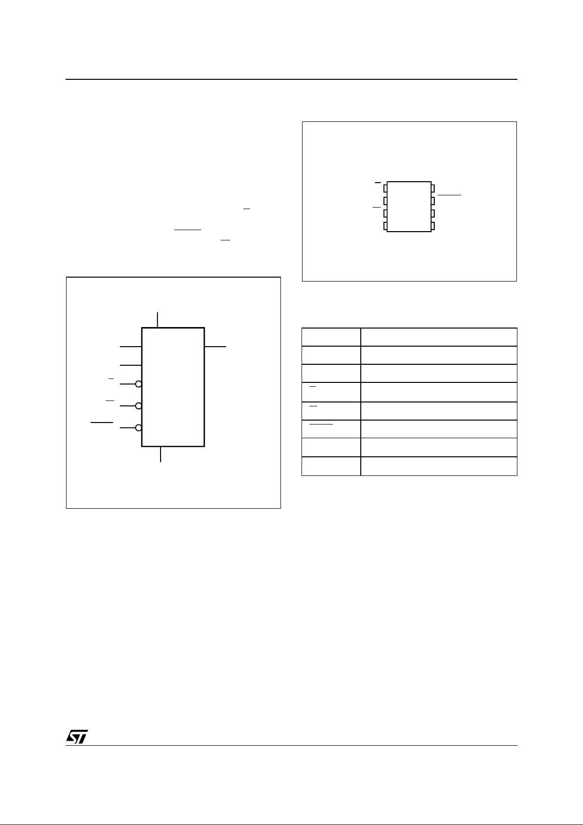
SUMMARY DESCRIPTION
The M95040 is a 4 Kbit (512 x 8) electrically erasable programmable memory (EEPROM), accessed by a high speed SPI-compatible bus. The other
members of the family (M95020 and M95010 ) are
identical, though proportionally smaller (2 and 1
Kbit, respe c ti v e ly).
Each device is accessed by a sim ple serial interface that is SPI-compatible. The bus signals are C,
D and Q, as shown in Table 2. and F igure 2..
The device is selected when Chip Select (S
en Low. Communications with the devi ce can be
interrupted using Hold (HOLD
). WRITE instruc-
tions are disabled by Write Protect (W
Figure 2. Logic Diagram
V
CC
D
C
S
W
M95xxx
) is tak-
).
Q
M95040, M95020, M95010
Figure 3. DIP, SO and TSSOP Connections
M95xxx
SV
1
2
W
3
4
SS
Note: See PACKAGE MECHANICAL section for package dimen-
sions, and how to ident i fy pi n-1.
Table 2. Signal Names
C Serial Clock
D Serial Data Input
Q Serial Data Output
S
Write Protect
W
Chip Select
8
7
6
5
AI01790D
CC
HOLDQ
C
DV
HOLD
HOLD
Hold
V
CC
V
V
SS
AI01789C
SS
Supply Voltage
Ground
5/37

M95040, M95020, M95010
SIGNAL DESCRIPTION
During all operations, VCC must be held stable and
within the specified valid range: V
(max).
V
CC
All of the input and output signals can be held High
or Low (according to voltage s of V
, as specified in Table 13. to Table 17.). These
V
OL
signals are described next.
Serial Data Output (Q). This output signal is
used to transfer data serially out of the device.
Data is shifted out on the falling edge of Serial
Clock (C).
Serial Data Input (D). This input signal is used to
transfer data serially into the device. It receives instructions, addresses, and the data to be written.
Values are latched on the rising edge of Serial
Clock (C).
Serial Clock (C). This input signal provides the
timing of the serial interface. Instructions, addresses, or data present at Serial Data Input (D) are
latched on the rising edge of Serial Clock (C). Data
on Serial Data Output (Q) changes after the falling
edge of Serial Clock (C).
(min) to
CC
, VOH, VIL or
IH
Chip Select (S
). When this input signal is High,
the device is des elected and Serial Data Ou tput
(Q) is at high impedance. Unless an internal Write
cycle is in progress, the device will be in the Standby Power mode. Drivi ng Chip Select ( S
) Low selects the device, placing it in the Active Power
mode.
After Power-up, a falling edge on Chip Select (S
is required prior to the start of any instruction.
Hold (HOLD
). The Hold (HOLD) signal is used to
pause any serial communications with the device
without deselecting the device.
During the Hold condition, the Serial Data Output
(Q) is high impedanc e, and Serial D ata Input (D)
and Serial Clock (C) are Don’t Care.
To start the Hold condition, the device must be selected, wit h Ch ip Select ( S
Write Protect (W
). This input signal is used to
) driven Low.
control whether the memory is write protected.
When Write Protect (W
) is held Low, writes to the
memory are disabled, but other operations remain
enabled. Write Protect (W
) must either be driven
High or Low, but must not be left floating.
)
6/37
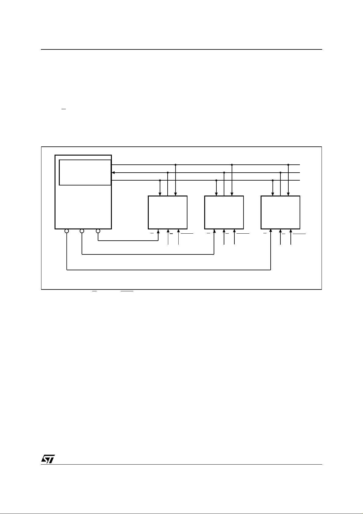
CONNECTI NG TO THE SPI BUS
These devices are fully compatible with the SPI
protocol.
All instructions, addresses and input data bytes
are shifted in to the device, most significant bit
first. The Serial Data Input (D) is sampled on the
first rising edge of the Serial Clock (C) after Chip
Selec t ( S
) goes Low.
All output data bytes are shifted out of the device,
most significant bit first. The Serial Data Output
Figure 4. Bus Master and Memory Devices on the SPI Bus
(Q) is latched on the first fa lling edge of the Serial
Clock (C) after the instruction (such as the Read
from Memory Array and Read Status Re gister instructions) have been clocked into the device.
Figure 4 . shows three devices, con nected to an
MCU, on a SPI bus. Only one device is selected at
a time, so only one de vice drives the Serial Data
Output (Q) line at a time, all the o thers be ing high
impedance.
M95040, M95020, M95010
SPI Interface with
(CPOL, CPHA) =
(0, 0) or (1, 1)
Bus Master
(ST6, ST7, ST9,
ST10, Others)
CS3 CS2 CS1
Note: The Write Protect (W) and Hold (HOLD) signals should be dri ven, High or Low as appropriat e.
SDO
SDI
SCK
CQD
SPI Memory
Device
S
CQD
SPI Memory
Device
HOLD
W
S
HOLD
W
CQD
SPI Memory
Device
S
W
AI03746D
HOLD
7/37

M95040, M95020, M95010
SPI Modes
These devices can be drive n by a microcont roller
with its SPI peripheral running in either of the two
following modes:
– CPOL=0, CPHA=0
– CPOL=1, CPHA=1
For these two modes, input data is latc hed in on
the rising edge of Serial Clock (C), and output data
Figure 5. SPI Mo de s S upported
CPHA
CPOL
0
0
1
1
C
C
D
Q
MSB
is avai lable from t he falling edge of S erial Clock
(C).
The difference between the two modes, as shown
in Figure 5., is the clock polarity when the bus
master is in Stand-by mode and not transferring
data:
– C remains at 0 for (CPOL=0, CPHA=0)
– C remains at 1 for (CPOL=1, CPHA=1)
MSB
AI01438B
8/37
OPERATING FEA T URES
Power-up
When the power supply is turned on, V
from V
During this time, the Chip Select (S
lowed to follow the V
to VCC.
SS
) must be al-
voltage. It must not be al-
CC
lowed to float, but should be connected to V
a suitable pull-up resistor.
As a built in safety feature, Chip Select (S
sensitive as well a s level sens itive. After P owerup, the device does not become s elected until a
falling edge has first been detected on Chip Select
). This ensures that Ch ip Select (S) must have
(S
been High, prior to going Low to start the first operation.
Power-down
At Power-down, the device must be deselected.
Chip Select (S
voltage applied on V
) should be allowed to follow the
.
CC
Active Power and Standb y Power M ode s
When Chip Select (S
) is Low, the device is selected, and in the Active Power mode. The device
consumes I
, as specified in Table 13. to Table
CC
17..
When Chip Select (S
) is High, the device is deselected. If an Erase/Write cycle is not currently in
progress, the device then goes in to the Standby
rises
CC
via
CC
) is edge
M95040, M95020, M95010
Power mode, and the device cons umption drops
CC1
.
) signal is used to pause any se-
) Low.
to I
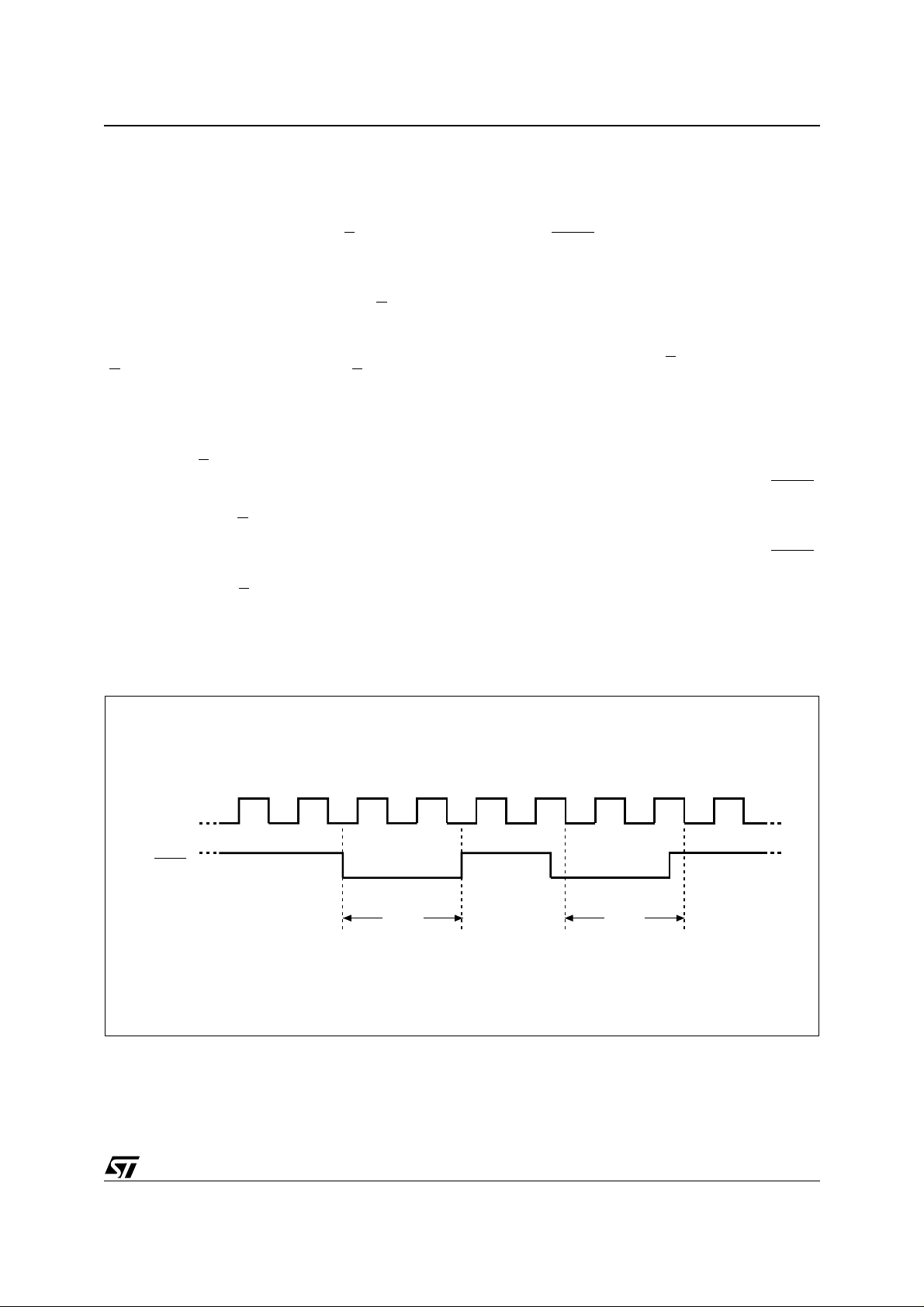
Hold Condition
The Hold (HOLD
rial communications with the device without resetting the clocking sequence.
During the Hold condition, the Serial Data Output
(Q) is high impedanc e, and Serial D ata Input (D)
and Serial Clock (C) are Don’t Care.
To enter the Hold condition, the device must be
selecte d, with Chip Se lec t (S
Normally, the device is kept selected, for the whole
duration of the Hold condition. Deselecting the device while it is in the Hold condition, has the effect
of resetting the state of the device, and this mechanism can be used if it is required to reset any processes that had been in progress.
The Hold condition starts when the Hold (HOLD
signal is driven Low at the same time as Serial
Clock (C) already being Low (as shown in Figure
6.).
The Hold condition ends when the Hold (HOLD
signal is driven High at the same time as Serial
Clock (C) already being Low.
Figure 6 . also shows what happens if the rising
and falling edges are not timed to coincide with
Serial Clock (C) being Low.
)
)
Figure 6. Hold Condition Activation
C
HOLD
Hold
Condition
Hold
Condition
AI02029D
9/37

M95040, M95020, M95010
Status Register
Figure 7. shows the position of the Status Register
in the control logic of the device. This register contains a number of c ontrol bits and status bits, as
shown in Table 3..
Bits b7, b6, b5 and b4 are always read as 1.
WIP bit. The Write In Progress bit is a volatile
read-only bit that is automatically set and reset by
the internal logic of the device. When s et to a 1 , it
indicates that the memory is busy with a Write cycle.
WEL bit. The Write Enable Latch bit is a vol atile
read-only bit that is set and reset by specific instructions. When reset to 0, no WRITE or WRSR
instructions are accepted by the device.
BP1, BP0 bits. The Block Protect bits are nonvolatile read-write bits. These bits define the area
of memory that is protected against the execution
of Write cycles, as summarized in Table 4..
Table 3. Status Register Format
b7 b0
1 1 1 1 BP1 BP0 WEL WIP
Block Protect Bits
Write Enable Latch Bit
Write In Progress Bit
Data Protec ti on a n d Protocol Cont rol
To help protect t he d ev ice from data corruption in
noisy or poorly controlled environments, a number
of safety features have been built in to the device.
The main security measures can be summarized
as follows:
– The WEL bit is reset at power-up.
– Chip Select (S
) must rise after the eighth clock
count (or multiple thereof) in order to start a
non-volatile Write cycle (in the memory array
or in the Status Register).
– Accesses to the memory array are ignored
during the non-volatile programming cycle,
and the programming cycle continues
unaffected.
– Invalid Chip Select (S
) and Hold (HOLD)
transitions are ignored.
For any instruction to be accepted and executed,
Chip Select (S
) must be driven High after the rising
edge of Serial Clock (C) that latches the last bit of
the instruction, and before the next rising edge of
Serial Clock (C).
For this, “the last bit of the instruction” can be the
eighth bit of the instruction code, or the ei ghth bit
of a data byte, depending on the instruction (except in the case of RDSR and READ instructions).
Moreover, the "next rising edge of CLOCK" might
(or might not) be the next bus transaction for some
other device on the bus.
When a Write cycle is in progress, the device protects it against external interruption by ignoring
any subsequent READ, WRITE or WRSR instruction until the presen t cycl e is complete.
Table 4. Write-Protected Block Size
Status Register Bits
Protected Block
BP1 BP0 M95040 M95020 M95010
0 0 none none none none
0 1 Upper quarter 180h - 1FFh C0h - FFh 60h - 7Fh
1 0 Upper half 100h - 1FFh 80h - FFh 40h - 7Fh
1 1 Whole memory 000h - 1FFh 00h - FFh 00h - 7Fh
10/37
Array Addresses Protected
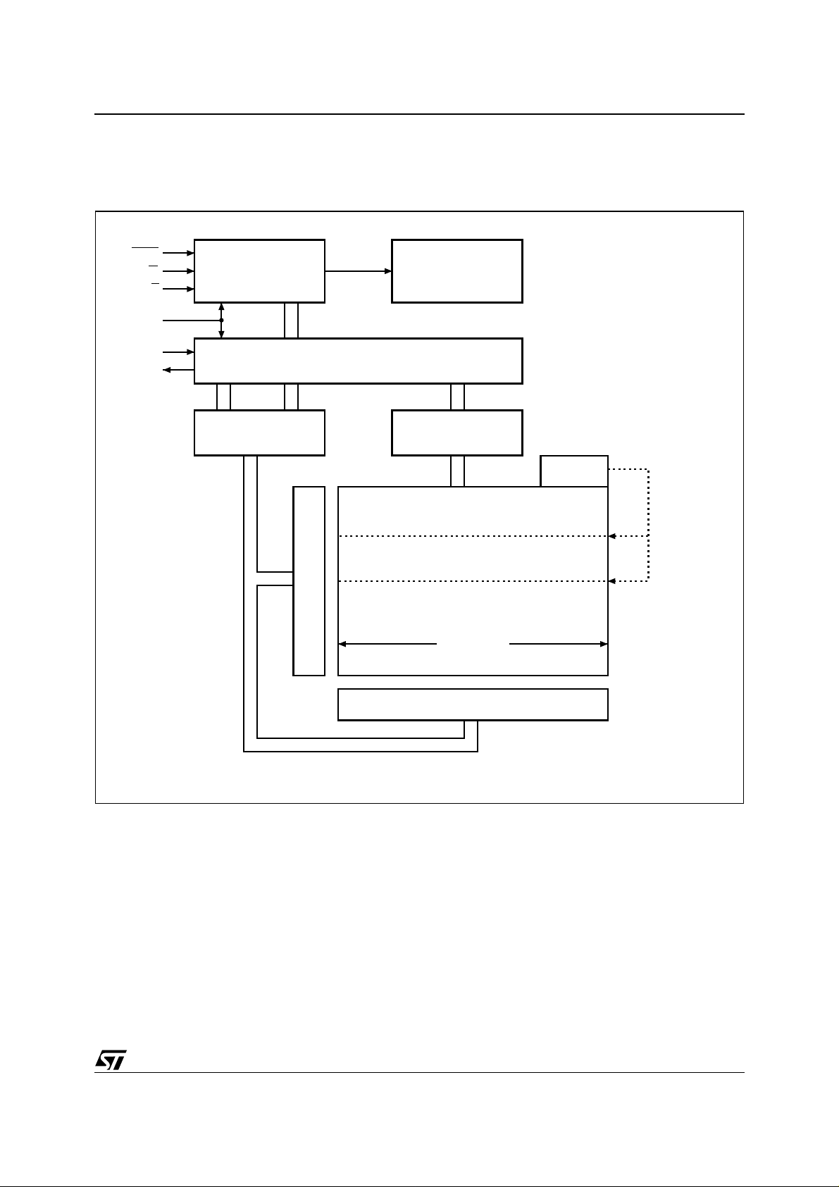
MEMOR Y ORGANIZATION
The memory is organized as shown in Figure 7..
Figure 7. Block Diagram
M95040, M95020, M95010
HOLD
W
S
C
D
Q
Control Logic
I/O Shift Register
Address Register
and Counter
Y Decoder
High Voltage
Generator
Data
Register
1 Page
Status
Register
Size of the
Read only
EEPROM
area
X Decoder
AI01272C
11/37

M95040, M95020, M95010
INSTRUCTIONS
Each instruction starts with a single-byte code, as
summarized in Table 5..
If an invalid instruction is s ent (one not con tained
in Table 5.), the device automatically deselects itself.
Table 5. Instruction Set
Instruc
tion
WREN Write Enable 0000 X110
WRDI Write Disable 0000 X100
RDSR Read Status Register 0000 X101
WRSR Write Status Register 0000 X001
READ Read from Memory Array
WRITE Write to Memory Array
Note: 1. A8 = 1 for the upper half of the memory array of the
M95040, and 0 for the lower half, and is Don’t Care fo r
other devices.
2. X = Don’ t Care.
Description
Instruction
Format
0000 A
0000 A
8
8
011
010
12/37
 Loading...