

查询M95010供应商
4Kbit, 2Kbit and 1Kbit Serial SPI Bus EEPROM
FEAT URES SUM MAR Y
■ Compatible with SPI Bus Serial Interface
(Positive Clock SPI Modes)
■ Single Supply Voltage:
– 4.5 to 5.5V for M950x0
– 2.5 to 5.5V for M950x0-W
– 1.8 to 5.5V for M950x0-R
■ High Speed
– 10MHz Clock Rate, 5ms Write Time
■ Status Register
■ BYTE and PAGE WRITE (up to 16 Bytes)
■ Self-Timed Programming Cycle
■ Adjustable Size Read-Only EEPROM Area
■ Enhanced ESD Protection
■ More than 1 Million Erase/Write Cycles
■ More than 40-Year Data Retention
M95040
M95020, M95010
With High Speed Clock
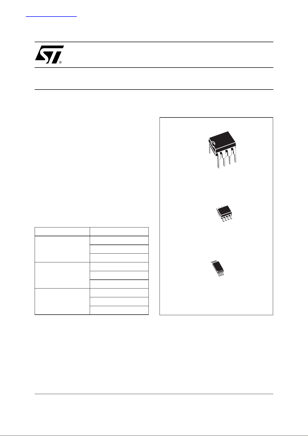
Figure 1. Packages
8
1
PDIP8 (BN)
8
Table 1. Product List
Reference Part Number
M95040
M95020
M95010
M95040
M95040-W
M95040-R
M95020
M95020-W
M95020-R
M95010
M95010-W
M95010-R
1
SO8 (MN)
150 mil width
TSSOP8 (DW)
169 mil width
1/37October 2004

M95040, M95020, M95010
TABLE OF CONTENTS
FEATURES SUMMARY . . . . . . . . . . . . . . . . . . . . . . . . . . . . . . . . . . . . . . . . . . . . . . . . . . . . . . . . . . . . . 1
Table 1. Product List . . . . . . . . . . . . . . . . . . . . . . . . . . . . . . . . . . . . . . . . . . . . . . . . . . . . . . . . . . . . 1
Figure 1. Packages. . . . . . . . . . . . . . . . . . . . . . . . . . . . . . . . . . . . . . . . . . . . . . . . . . . . . . . . . . . . . . 1
SUMMARY DESCRIPTION. . . . . . . . . . . . . . . . . . . . . . . . . . . . . . . . . . . . . . . . . . . . . . . . . . . . . . . . . . . 5
Figure 2. Logic Diagram . . . . . . . . . . . . . . . . . . . . . . . . . . . . . . . . . . . . . . . . . . . . . . . . . . . . . . . . . . 5
Figure 3. DIP, SO and TSSOP Connections . . . . . . . . . . . . . . . . . . . . . . . . . . . . . . . . . . . . . . . . . . 5
Table 2. Signal Names . . . . . . . . . . . . . . . . . . . . . . . . . . . . . . . . . . . . . . . . . . . . . . . . . . . . . . . . . . 5
SIGNAL DESCRIPTION . . . . . . . . . . . . . . . . . . . . . . . . . . . . . . . . . . . . . . . . . . . . . . . . . . . . . . . . . . . . . 6
Serial Data Output (Q). . . . . . . . . . . . . . . . . . . . . . . . . . . . . . . . . . . . . . . . . . . . . . . . . . . . . . . . . . . . 6
Serial Data Input (D) . . . . . . . . . . . . . . . . . . . . . . . . . . . . . . . . . . . . . . . . . . . . . . . . . . . . . . . . . . . . . 6
Serial Clock (C) . . . . . . . . . . . . . . . . . . . . . . . . . . . . . . . . . . . . . . . . . . . . . . . . . . . . . . . . . . . . . . . . .6
Chip Select (S) . . . . . . . . . . . . . . . . . . . . . . . . . . . . . . . . . . . . . . . . . . . . . . . . . . . . . . . . . . . . . . . . . 6
Hold (HOLD) . . . . . . . . . . . . . . . . . . . . . . . . . . . . . . . . . . . . . . . . . . . . . . . . . . . . . . . . . . . . . . . . . . . 6
Write Protect (W). . . . . . . . . . . . . . . . . . . . . . . . . . . . . . . . . . . . . . . . . . . . . . . . . . . . . . . . . . . . . . . . 6
CONNECTING TO THE SPI BUS . . . . . . . . . . . . . . . . . . . . . . . . . . . . . . . . . . . . . . . . . . . . . . . . . . . . . . 7
Figure 4. Bus Master and Memory Devices on the SPI Bus. . . . . . . . . . . . . . . . . . . . . . . . . . . . . . . 7
SPI Modes . . . . . . . . . . . . . . . . . . . . . . . . . . . . . . . . . . . . . . . . . . . . . . . . . . . . . . . . . . . . . . . . . . . . 8
Figure 5. SPI Modes Supported . . . . . . . . . . . . . . . . . . . . . . . . . . . . . . . . . . . . . . . . . . . . . . . . . . . . 8
OPERATING FEATURES. . . . . . . . . . . . . . . . . . . . . . . . . . . . . . . . . . . . . . . . . . . . . . . . . . . . . . . . . . . . 9
Power-up . . . . . . . . . . . . . . . . . . . . . . . . . . . . . . . . . . . . . . . . . . . . . . . . . . . . . . . . . . . . . . . . . . . . . 9
Power-down. . . . . . . . . . . . . . . . . . . . . . . . . . . . . . . . . . . . . . . . . . . . . . . . . . . . . . . . . . . . . . . . . . . 9
Active Power and Standby Power Modes. . . . . . . . . . . . . . . . . . . . . . . . . . . . . . . . . . . . . . . . . . . 9
Hold Condition. . . . . . . . . . . . . . . . . . . . . . . . . . . . . . . . . . . . . . . . . . . . . . . . . . . . . . . . . . . . . . . . . 9
Figure 6. Hold Condition Activation. . . . . . . . . . . . . . . . . . . . . . . . . . . . . . . . . . . . . . . . . . . . . . . . . . 9
Status Register . . . . . . . . . . . . . . . . . . . . . . . . . . . . . . . . . . . . . . . . . . . . . . . . . . . . . . . . . . . . . . . 10
WIP bit. . . . . . . . . . . . . . . . . . . . . . . . . . . . . . . . . . . . . . . . . . . . . . . . . . . . . . . . . . . . . . . . . . . . . . . 10
WEL bit . . . . . . . . . . . . . . . . . . . . . . . . . . . . . . . . . . . . . . . . . . . . . . . . . . . . . . . . . . . . . . . . . . . . . . 10
BP1, BP0 bits . . . . . . . . . . . . . . . . . . . . . . . . . . . . . . . . . . . . . . . . . . . . . . . . . . . . . . . . . . . . . . . . . 10
Table 3. Status Register Format . . . . . . . . . . . . . . . . . . . . . . . . . . . . . . . . . . . . . . . . . . . . . . . . . . 10
Data Protection and Protocol Control. . . . . . . . . . . . . . . . . . . . . . . . . . . . . . . . . . . . . . . . . . . . . 10
Table 4. Write-Protected Block Size . . . . . . . . . . . . . . . . . . . . . . . . . . . . . . . . . . . . . . . . . . . . . . .10
MEMORY ORGANIZATION . . . . . . . . . . . . . . . . . . . . . . . . . . . . . . . . . . . . . . . . . . . . . . . . . . . . . . . . . 11
Figure 7. Block Diagram . . . . . . . . . . . . . . . . . . . . . . . . . . . . . . . . . . . . . . . . . . . . . . . . . . . . . . . . . 11
INSTRUCTIONS . . . . . . . . . . . . . . . . . . . . . . . . . . . . . . . . . . . . . . . . . . . . . . . . . . . . . . . . . . . . . . . . . . 12
Table 5. Instruction Set . . . . . . . . . . . . . . . . . . . . . . . . . . . . . . . . . . . . . . . . . . . . . . . . . . . . . . . . . 12
Write Enable (WREN) . . . . . . . . . . . . . . . . . . . . . . . . . . . . . . . . . . . . . . . . . . . . . . . . . . . . . . . . . . 13
Figure 8. Write Enable (WREN) Sequence. . . . . . . . . . . . . . . . . . . . . . . . . . . . . . . . . . . . . . . . . . . 13
2/37

M95040, M95020, M95010
Write Disable (WRDI). . . . . . . . . . . . . . . . . . . . . . . . . . . . . . . . . . . . . . . . . . . . . . . . . . . . . . . . . . . 13
Figure 9. Write Disable (WRDI) Sequence. . . . . . . . . . . . . . . . . . . . . . . . . . . . . . . . . . . . . . . . . . . 13
Read Status Register (RDSR). . . . . . . . . . . . . . . . . . . . . . . . . . . . . . . . . . . . . . . . . . . . . . . . . . . . 14
WIP bit. . . . . . . . . . . . . . . . . . . . . . . . . . . . . . . . . . . . . . . . . . . . . . . . . . . . . . . . . . . . . . . . . . . . . . . 14
WEL bit . . . . . . . . . . . . . . . . . . . . . . . . . . . . . . . . . . . . . . . . . . . . . . . . . . . . . . . . . . . . . . . . . . . . . . 14
BP1, BP0 bits . . . . . . . . . . . . . . . . . . . . . . . . . . . . . . . . . . . . . . . . . . . . . . . . . . . . . . . . . . . . . . . . . 14
Figure 10.Read Status Register (RDSR) Sequence . . . . . . . . . . . . . . . . . . . . . . . . . . . . . . . . . . . . 14
Write Status Register (WRSR) . . . . . . . . . . . . . . . . . . . . . . . . . . . . . . . . . . . . . . . . . . . . . . . . . . . 15
Figure 11.Write Status Register (WRSR) Sequence. . . . . . . . . . . . . . . . . . . . . . . . . . . . . . . . . . . . 15
Read from Memory Array (READ) . . . . . . . . . . . . . . . . . . . . . . . . . . . . . . . . . . . . . . . . . . . . . . . . 16
Table 6. Address Range Bits. . . . . . . . . . . . . . . . . . . . . . . . . . . . . . . . . . . . . . . . . . . . . . . . . . . . . 16
Figure 12.Read from Memory Array (READ) Sequen ce . . . . . . . . . . . . . . . . . . . . . . . . . . . . . . . . . 16
Write to Memory Array (WRITE). . . . . . . . . . . . . . . . . . . . . . . . . . . . . . . . . . . . . . . . . . . . . . . . . .17
Figure 13.Byte Write (WRITE) Sequence . . . . . . . . . . . . . . . . . . . . . . . . . . . . . . . . . . . . . . . . . . . . 17
Figure 14.Page Write (WRITE) Sequence . . . . . . . . . . . . . . . . . . . . . . . . . . . . . . . . . . . . . . . . . . . 18
POWER-UP AND DELIVERY STATE. . . . . . . . . . . . . . . . . . . . . . . . . . . . . . . . . . . . . . . . . . . . . . . . . . 19
Power-up State . . . . . . . . . . . . . . . . . . . . . . . . . . . . . . . . . . . . . . . . . . . . . . . . . . . . . . . . . . . . . . . 19
Initial Delivery State . . . . . . . . . . . . . . . . . . . . . . . . . . . . . . . . . . . . . . . . . . . . . . . . . . . . . . . . . . . 19
MAXIMUM RATING. . . . . . . . . . . . . . . . . . . . . . . . . . . . . . . . . . . . . . . . . . . . . . . . . . . . . . . . . . . . . . . . 20
Table 7. Absolute Maximum Ratings. . . . . . . . . . . . . . . . . . . . . . . . . . . . . . . . . . . . . . . . . . . . . . . 20
DC AND AC PARAMETERS. . . . . . . . . . . . . . . . . . . . . . . . . . . . . . . . . . . . . . . . . . . . . . . . . . . . . . . . . 2 1
Table 8. Operating Conditions (M950x0). . . . . . . . . . . . . . . . . . . . . . . . . . . . . . . . . . . . . . . . . . . . 21
Table 9. Operating Conditions (M950x0-W) . . . . . . . . . . . . . . . . . . . . . . . . . . . . . . . . . . . . . . . . . 21
Table 10. Operating Conditions (M950x 0-R). . . . . . . . . . . . . . . . . . . . . . . . . . . . . . . . . . . . . . . . . . 21
Table 11. AC Measurement Condition s. . . . . . . . . . . . . . . . . . . . . . . . . . . . . . . . . . . . . . . . . . . . . .21
Figure 15.AC Measurement I/O Waveform. . . . . . . . . . . . . . . . . . . . . . . . . . . . . . . . . . . . . . . . . . . 21
Table 12.Capacitance. . . . . . . . . . . . . . . . . . . . . . . . . . . . . . . . . . . . . . . . . . . . . . . . . . . . . . . . . . . 22
Table 13. DC Characteristics (M950x0, Device Grade 6) . . . . . . . . . . . . . . . . . . . . . . . . . . . . . . . . 22
Table 14. DC Characteristics (M950x0, Device Grade 3) . . . . . . . . . . . . . . . . . . . . . . . . . . . . . . . . 23
Table 15. DC Characteristics (M950x0-W, Device Grade 6). . . . . . . . . . . . . . . . . . . . . . . . . . . . . .23
Table 16. DC Characteristics (M950x0-W, Device Grade 3). . . . . . . . . . . . . . . . . . . . . . . . . . . . . .24
Table 17. DC Characteristics (M950x0-R). . . . . . . . . . . . . . . . . . . . . . . . . . . . . . . . . . . . . . . . . . . . 24
Table 18. AC Characteristics (M950x0, Device Grade 6) . . . . . . . . . . . . . . . . . . . . . . . . . . . . . . . . 25
Table 19. AC Characteristics (M950x0, Device Grade 3) . . . . . . . . . . . . . . . . . . . . . . . . . . . . . . . . 26
Table 20. AC Characteristics (M950x0-W, Device Grade 6) . . . . . . . . . . . . . . . . . . . . . . . . . . . . . . 27
Table 21. AC Characteristics (M950x0-W, Device Grade 3) . . . . . . . . . . . . . . . . . . . . . . . . . . . . . . 28
Table 22. AC Characteristics (M950x0-R). . . . . . . . . . . . . . . . . . . . . . . . . . . . . . . . . . . . . . . . . . . . 29
Figure 16.Serial Input Timing . . . . . . . . . . . . . . . . . . . . . . . . . . . . . . . . . . . . . . . . . . . . . . . . . . . . . 30
Figure 17.Hold Timing. . . . . . . . . . . . . . . . . . . . . . . . . . . . . . . . . . . . . . . . . . . . . . . . . . . . . . . . . . . 30
Figure 18.Output Timing . . . . . . . . . . . . . . . . . . . . . . . . . . . . . . . . . . . . . . . . . . . . . . . . . . . . . . . . . 31
PACKAGE MECHANICAL . . . . . . . . . . . . . . . . . . . . . . . . . . . . . . . . . . . . . . . . . . . . . . . . . . . . . . . . . . 32
Figure 19.PDIP8 – 8 pin Plastic DIP, 0.25mm lead frame, Package Outline . . . . . . . . . . . . . . . . . 32
3/37

M95040, M95020, M95010
Table 23. PDIP8 – 8 pin Plastic DIP, 0.25mm lead frame, Package Mechanical Data . . . . . . . . . . 32
Figure 20.SO8 narrow – 8 lead Plastic Small Outline, 150 mils body width, Package Outline . . . . 33
Table 24. SO8 narrow – 8 lead Plastic Small Outline, 150 mils body width, Package Mechanical Data
33
Figure 21.TSSOP8 – 8 lead Thin Shrink Small Outline, Package Outline . . . . . . . . . . . . . . . . . . . 34
Table 25. TSSOP8 – 8 lead Thin Shrink Sma ll Outline, Packag e Mechanica l Data . . . . . . . . . . . . 34
PART NUMBERING . . . . . . . . . . . . . . . . . . . . . . . . . . . . . . . . . . . . . . . . . . . . . . . . . . . . . . . . . . . . . . . 35
Table 26.Ordering Information Scheme . . . . . . . . . . . . . . . . . . . . . . . . . . . . . . . . . . . . . . . . . . . . . 35
Table 27. How to Identify Present and Previous Pro ducts by the Process Identi fication Letter . . . 35
REVISION HISTORY. . . . . . . . . . . . . . . . . . . . . . . . . . . . . . . . . . . . . . . . . . . . . . . . . . . . . . . . . . . . . . . 36
Table 28. Document Revision History. . . . . . . . . . . . . . . . . . . . . . . . . . . . . . . . . . . . . . . . . . . . . . . 36
4/37
SUMMARY DESCRIPTION
The M95040 is a 4 Kbit (512 x 8) electrically erasable programmable memory (EEPROM), accessed by a high speed SPI-compatible bus. The other
members of the family (M95020 and M95010 ) are
identical, though proportionally smaller (2 and 1
Kbit, respe c ti v e ly).
Each device is accessed by a sim ple serial interface that is SPI-compatible. The bus signals are C,
D and Q, as shown in Table 2. and F igure 2..
The device is selected when Chip Select (S
en Low. Communications with the devi ce can be
interrupted using Hold (HOLD
). WRITE instruc-
tions are disabled by Write Protect (W
Figure 2. Logic Diagram
V
CC
D
C
S
W
M95xxx
) is tak-
).
Q
M95040, M95020, M95010
Figure 3. DIP, SO and TSSOP Connections
M95xxx
SV
1
2
W
3
4
SS
Note: See PACKAGE MECHANICAL section for package dimen-
sions, and how to ident i fy pi n-1.
Table 2. Signal Names
C Serial Clock
D Serial Data Input
Q Serial Data Output
S
Write Protect
W
Chip Select
8
7
6
5
AI01790D
CC
HOLDQ
C
DV
HOLD
HOLD
Hold
V
CC
V
V
SS
AI01789C
SS
Supply Voltage
Ground
5/37

M95040, M95020, M95010
SIGNAL DESCRIPTION
During all operations, VCC must be held stable and
within the specified valid range: V
(max).
V
CC
All of the input and output signals can be held High
or Low (according to voltage s of V
, as specified in Table 13. to Table 17.). These
V
OL
signals are described next.
Serial Data Output (Q). This output signal is
used to transfer data serially out of the device.
Data is shifted out on the falling edge of Serial
Clock (C).
Serial Data Input (D). This input signal is used to
transfer data serially into the device. It receives instructions, addresses, and the data to be written.
Values are latched on the rising edge of Serial
Clock (C).
Serial Clock (C). This input signal provides the
timing of the serial interface. Instructions, addresses, or data present at Serial Data Input (D) are
latched on the rising edge of Serial Clock (C). Data
on Serial Data Output (Q) changes after the falling
edge of Serial Clock (C).
(min) to
CC
, VOH, VIL or
IH
Chip Select (S
). When this input signal is High,
the device is des elected and Serial Data Ou tput
(Q) is at high impedance. Unless an internal Write
cycle is in progress, the device will be in the Standby Power mode. Drivi ng Chip Select ( S
) Low selects the device, placing it in the Active Power
mode.
After Power-up, a falling edge on Chip Select (S
is required prior to the start of any instruction.
Hold (HOLD
). The Hold (HOLD) signal is used to
pause any serial communications with the device
without deselecting the device.
During the Hold condition, the Serial Data Output
(Q) is high impedanc e, and Serial D ata Input (D)
and Serial Clock (C) are Don’t Care.
To start the Hold condition, the device must be selected, wit h Ch ip Select ( S
Write Protect (W
). This input signal is used to
) driven Low.
control whether the memory is write protected.
When Write Protect (W
) is held Low, writes to the
memory are disabled, but other operations remain
enabled. Write Protect (W
) must either be driven
High or Low, but must not be left floating.
)
6/37
CONNECTI NG TO THE SPI BUS
These devices are fully compatible with the SPI
protocol.
All instructions, addresses and input data bytes
are shifted in to the device, most significant bit
first. The Serial Data Input (D) is sampled on the
first rising edge of the Serial Clock (C) after Chip
Selec t ( S
) goes Low.
All output data bytes are shifted out of the device,
most significant bit first. The Serial Data Output
Figure 4. Bus Master and Memory Devices on the SPI Bus
(Q) is latched on the first fa lling edge of the Serial
Clock (C) after the instruction (such as the Read
from Memory Array and Read Status Re gister instructions) have been clocked into the device.
Figure 4 . shows three devices, con nected to an
MCU, on a SPI bus. Only one device is selected at
a time, so only one de vice drives the Serial Data
Output (Q) line at a time, all the o thers be ing high
impedance.
M95040, M95020, M95010
SPI Interface with
(CPOL, CPHA) =
(0, 0) or (1, 1)
Bus Master
(ST6, ST7, ST9,
ST10, Others)
CS3 CS2 CS1
Note: The Write Protect (W) and Hold (HOLD) signals should be dri ven, High or Low as appropriat e.
SDO
SDI
SCK
CQD
SPI Memory
Device
S
CQD
SPI Memory
Device
HOLD
W
S
HOLD
W
CQD
SPI Memory
Device
S
W
AI03746D
HOLD
7/37
M95040, M95020, M95010
SPI Modes
These devices can be drive n by a microcont roller
with its SPI peripheral running in either of the two
following modes:
– CPOL=0, CPHA=0
– CPOL=1, CPHA=1
For these two modes, input data is latc hed in on
the rising edge of Serial Clock (C), and output data
Figure 5. SPI Mo de s S upported
CPHA
CPOL
0
0
1
1
C
C
D
Q
MSB
is avai lable from t he falling edge of S erial Clock
(C).
The difference between the two modes, as shown
in Figure 5., is the clock polarity when the bus
master is in Stand-by mode and not transferring
data:
– C remains at 0 for (CPOL=0, CPHA=0)
– C remains at 1 for (CPOL=1, CPHA=1)
MSB
AI01438B
8/37
OPERATING FEA T URES
Power-up
When the power supply is turned on, V
from V
During this time, the Chip Select (S
lowed to follow the V
to VCC.
SS
) must be al-
voltage. It must not be al-
CC
lowed to float, but should be connected to V
a suitable pull-up resistor.
As a built in safety feature, Chip Select (S
sensitive as well a s level sens itive. After P owerup, the device does not become s elected until a
falling edge has first been detected on Chip Select
). This ensures that Ch ip Select (S) must have
(S
been High, prior to going Low to start the first operation.
Power-down
At Power-down, the device must be deselected.
Chip Select (S
voltage applied on V
) should be allowed to follow the
.
CC
Active Power and Standb y Power M ode s
When Chip Select (S
) is Low, the device is selected, and in the Active Power mode. The device
consumes I
, as specified in Table 13. to Table
CC
17..
When Chip Select (S
) is High, the device is deselected. If an Erase/Write cycle is not currently in
progress, the device then goes in to the Standby
rises
CC
via
CC
) is edge
M95040, M95020, M95010
Power mode, and the device cons umption drops
CC1
.
) signal is used to pause any se-
) Low.
to I
Hold Condition
The Hold (HOLD
rial communications with the device without resetting the clocking sequence.
During the Hold condition, the Serial Data Output
(Q) is high impedanc e, and Serial D ata Input (D)
and Serial Clock (C) are Don’t Care.
To enter the Hold condition, the device must be
selecte d, with Chip Se lec t (S
Normally, the device is kept selected, for the whole
duration of the Hold condition. Deselecting the device while it is in the Hold condition, has the effect
of resetting the state of the device, and this mechanism can be used if it is required to reset any processes that had been in progress.
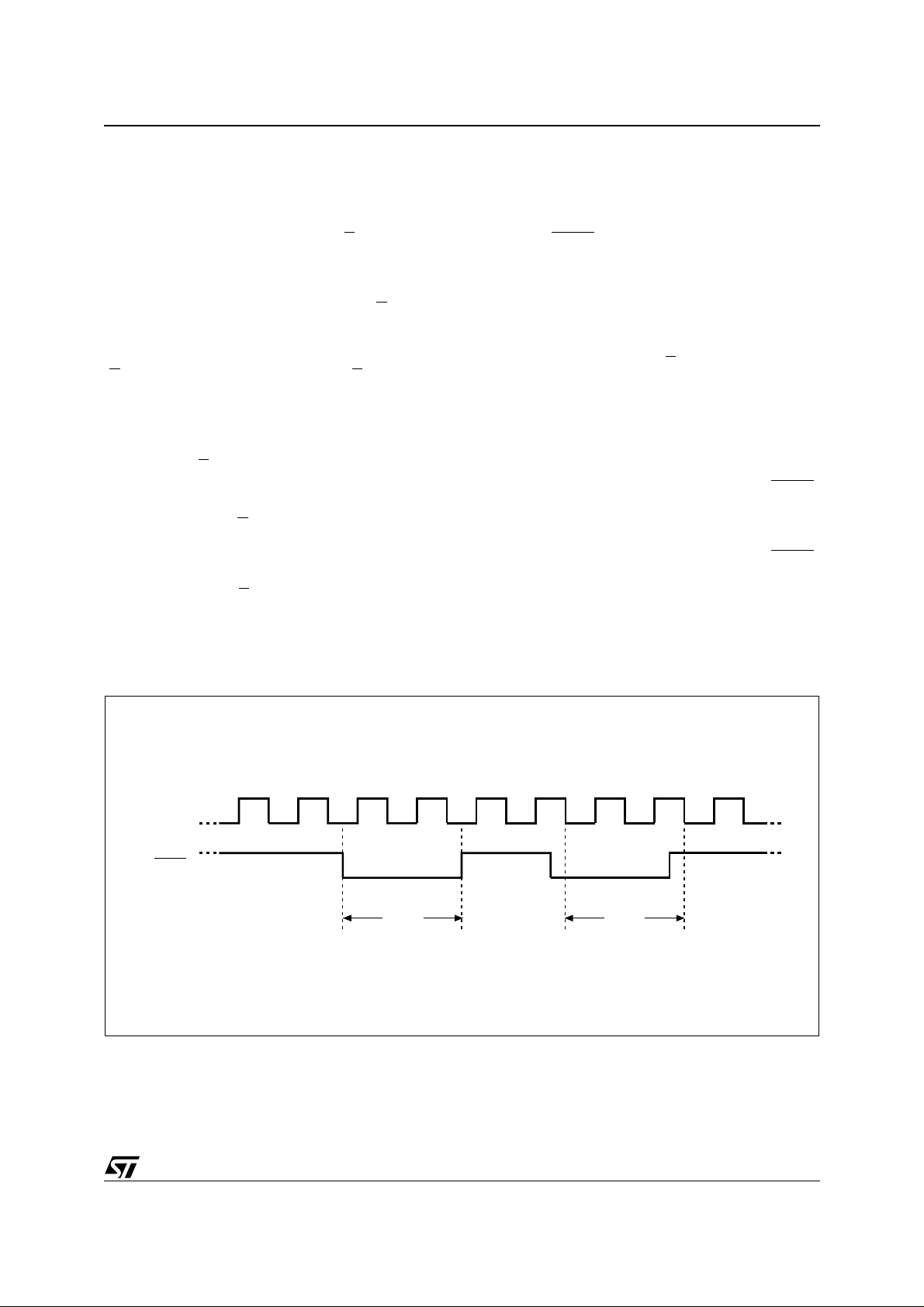
The Hold condition starts when the Hold (HOLD
signal is driven Low at the same time as Serial
Clock (C) already being Low (as shown in Figure
6.).
The Hold condition ends when the Hold (HOLD
signal is driven High at the same time as Serial
Clock (C) already being Low.
Figure 6 . also shows what happens if the rising
and falling edges are not timed to coincide with
Serial Clock (C) being Low.
)
)
Figure 6. Hold Condition Activation
C
HOLD
Hold
Condition
Hold
Condition
AI02029D
9/37
M95040, M95020, M95010
Status Register
Figure 7. shows the position of the Status Register
in the control logic of the device. This register contains a number of c ontrol bits and status bits, as
shown in Table 3..
Bits b7, b6, b5 and b4 are always read as 1.
WIP bit. The Write In Progress bit is a volatile
read-only bit that is automatically set and reset by
the internal logic of the device. When s et to a 1 , it
indicates that the memory is busy with a Write cycle.
WEL bit. The Write Enable Latch bit is a vol atile
read-only bit that is set and reset by specific instructions. When reset to 0, no WRITE or WRSR
instructions are accepted by the device.
BP1, BP0 bits. The Block Protect bits are nonvolatile read-write bits. These bits define the area
of memory that is protected against the execution
of Write cycles, as summarized in Table 4..
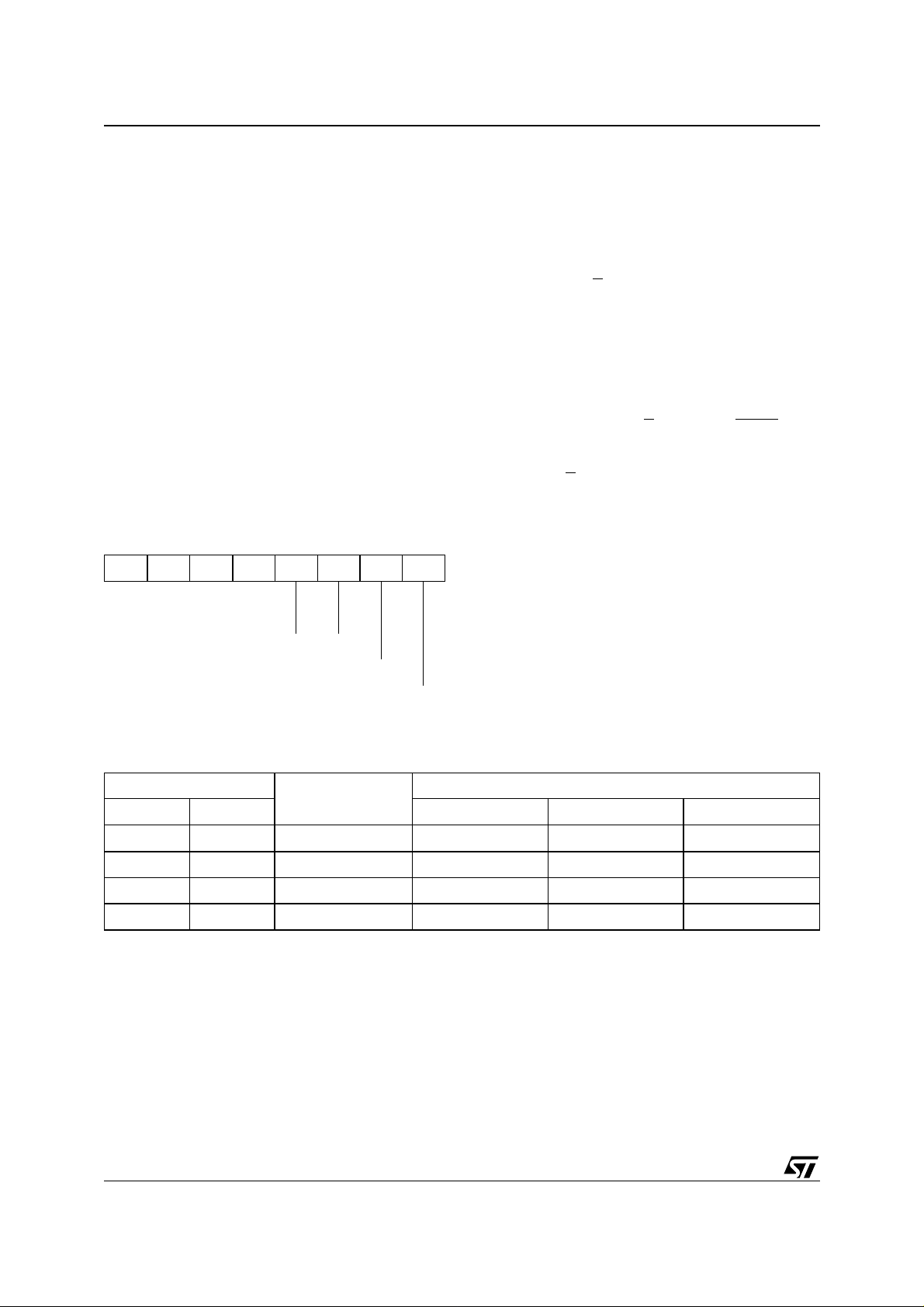
Table 3. Status Register Format
b7 b0
1 1 1 1 BP1 BP0 WEL WIP
Block Protect Bits
Write Enable Latch Bit
Write In Progress Bit
Data Protec ti on a n d Protocol Cont rol
To help protect t he d ev ice from data corruption in
noisy or poorly controlled environments, a number
of safety features have been built in to the device.
The main security measures can be summarized
as follows:
– The WEL bit is reset at power-up.
– Chip Select (S
) must rise after the eighth clock
count (or multiple thereof) in order to start a
non-volatile Write cycle (in the memory array
or in the Status Register).
– Accesses to the memory array are ignored
during the non-volatile programming cycle,
and the programming cycle continues
unaffected.
– Invalid Chip Select (S
) and Hold (HOLD)
transitions are ignored.
For any instruction to be accepted and executed,
Chip Select (S
) must be driven High after the rising
edge of Serial Clock (C) that latches the last bit of
the instruction, and before the next rising edge of
Serial Clock (C).
For this, “the last bit of the instruction” can be the
eighth bit of the instruction code, or the ei ghth bit
of a data byte, depending on the instruction (except in the case of RDSR and READ instructions).
Moreover, the "next rising edge of CLOCK" might
(or might not) be the next bus transaction for some
other device on the bus.
When a Write cycle is in progress, the device protects it against external interruption by ignoring
any subsequent READ, WRITE or WRSR instruction until the presen t cycl e is complete.
Table 4. Write-Protected Block Size
Status Register Bits
Protected Block
BP1 BP0 M95040 M95020 M95010
0 0 none none none none
0 1 Upper quarter 180h - 1FFh C0h - FFh 60h - 7Fh
1 0 Upper half 100h - 1FFh 80h - FFh 40h - 7Fh
1 1 Whole memory 000h - 1FFh 00h - FFh 00h - 7Fh
10/37
Array Addresses Protected
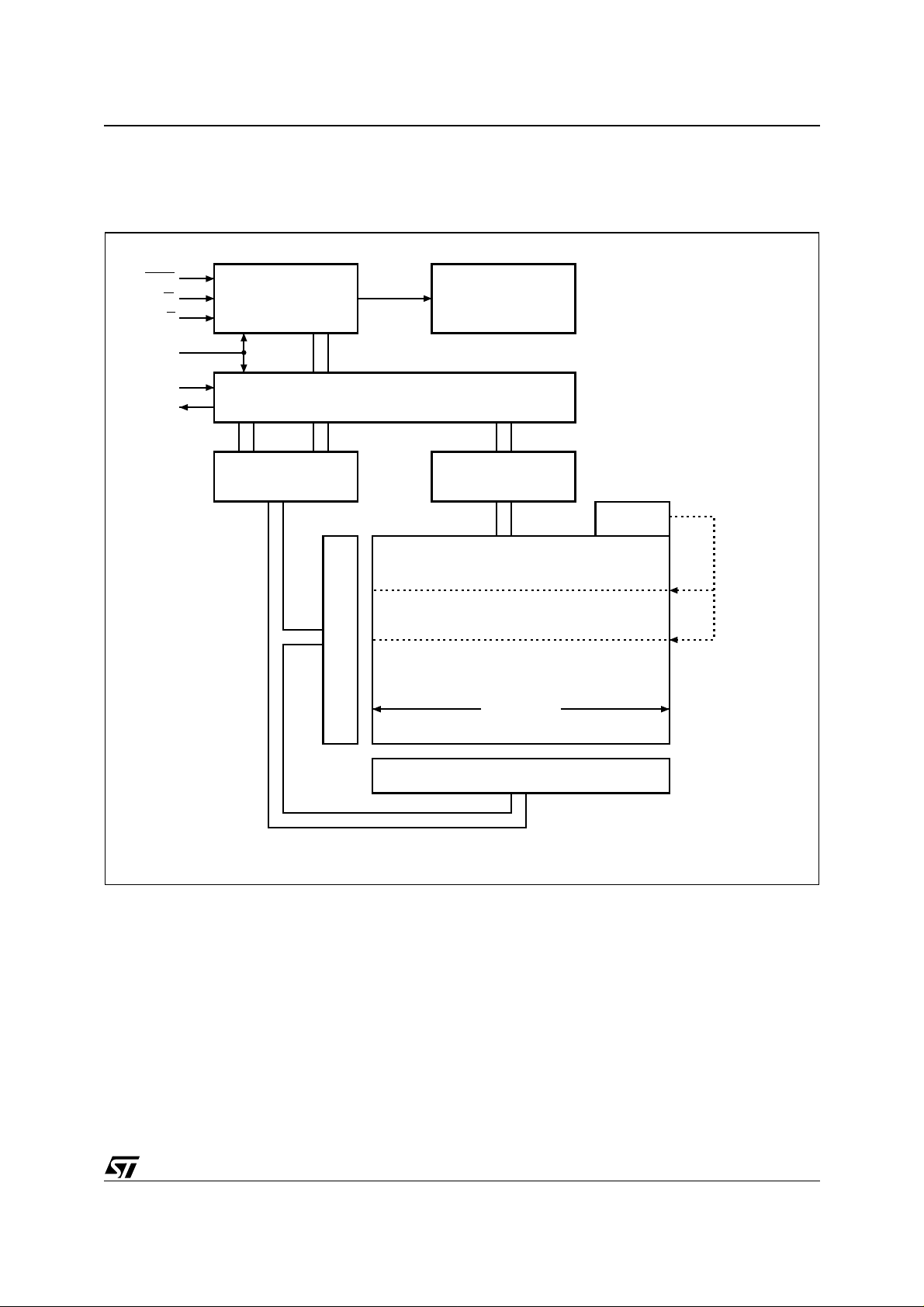
MEMOR Y ORGANIZATION
The memory is organized as shown in Figure 7..
Figure 7. Block Diagram
M95040, M95020, M95010
HOLD
W
S
C
D
Q
Control Logic
I/O Shift Register
Address Register
and Counter
Y Decoder
High Voltage
Generator
Data
Register
1 Page
Status
Register
Size of the
Read only
EEPROM
area
X Decoder
AI01272C
11/37
M95040, M95020, M95010
INSTRUCTIONS
Each instruction starts with a single-byte code, as
summarized in Table 5..
If an invalid instruction is s ent (one not con tained
in Table 5.), the device automatically deselects itself.
Table 5. Instruction Set
Instruc
tion
WREN Write Enable 0000 X110
WRDI Write Disable 0000 X100
RDSR Read Status Register 0000 X101
WRSR Write Status Register 0000 X001
READ Read from Memory Array
WRITE Write to Memory Array
Note: 1. A8 = 1 for the upper half of the memory array of the
M95040, and 0 for the lower half, and is Don’t Care fo r
other devices.
2. X = Don’ t Care.
Description
Instruction
Format
0000 A
0000 A
8
8
011
010
12/37

M95040, M95020, M95010
Write Enable (WREN)
The Write Enable Latch (WEL) bit must be set prior to each WRITE and WRSR instruction. The only
way to do this is to send a Write Enable instruction
to the device.
Figure 8. Write Enable (WREN) Sequence
S
0
C
D
High Impedance
Q
Write Disable (WRDI)
One way of resetting the Write Enable Latch
(WEL) bit is to send a Write Disable instruction to
the device.
As shown in Figure 9., to send this i nstruc tion t o
the devic e , C hip Selec t ( S
) is driven Low, and the
bits of the instruction byte are shifted in, on Serial
Data Input (D).
As shown in Figure 8., to send this instruction to
the devic e , C hip Selec t ( S
) is driven Low, and the
bits of the instruction byte are shifted in, on Serial
Data Input (D). The device then enters a wait
state. It waits for a the device to be deselected, by
Chip Selec t ( S
21 34567
Instruction
) being driven High.
AI01441D
The device then enters a wait state. It waits for a
the device to be deselected, by Chip Select (S
ing driven High.
The Write Enable Latch (WEL) bit, in fact, becomes reset by any of the following events:
–Power-up
– WRDI instruction execution
– WRSR instruction completion
– WRITE instruction completion
– Write Protect (W
) line being held Low.
) be-
Figure 9. Write Disable (WRDI) Sequence
S
C
D
Q
0
21 34567
Instruction
High Impedance
AI03790D
13/37

M95040, M95020, M95010
Read Status Register (RDSR)
One of the major uses of this inst ruction is to allow
the MCU to poll the state o f the Write I n Pr ogress
(WIP) bit. This is needed because the device wi ll
not accept further W RITE or WRSR i nstructions
when the previous Write cycle is not yet finished.
As shown in Figure 10., to send this instruction t o
the device, Chip Se l e ct (S
) is first driven Low. The
bits of the instruction byte are then shifted in, on
Serial Data Input (D). The current state of t he bi ts
in the Status Register is shifted out, on Serial Data
Out (Q). The Read Cycle is terminated by driving
Chip Selec t ( S
) High.
The Status Register may be read at any time, even
during a Write cycle (whether it be to the memory
area or to the Status Regist er). All bi ts of t he Status Register remain valid, and can be read using
the RDSR instruction. However, during the current
Write cycle, the values of the non-volatile bits
(BP0, BP1) become frozen at a constant value.
The updated value of these bits becomes available when a new RDSR instruction is executed, after completion of the Write cycle. On the other
hand, the two read-only bits (Write Enable Latch
(WEL), Write In Progress (WIP)) are dynamically
updated during the on-going Write cycle.
The status and control bits of t he Status Register
are as follows:
WIP bit. The Write In Progress (WIP) bit indicates
whether the memory is busy with a Write or Write
Status Register cycle. When set to 1, such a cycle
is in progress, when reset to 0 no such cycle is in
progress.
WEL bit. The Write Enable Latch (WEL) bit i ndicates the status of the internal Write Enable Latch.
When set to 1 the internal Write Enable Latch is
set, when set to 0 t he i nternal Write Enable La tch
is reset and no Write or Write Status Register instruction is accepted.
BP1, BP0 bits. The Block Protect (BP1, BP0) bits
are non-volatile. They define the size of the area to
be software protected against Write instructions.
These bits are written with the Write Status Register (WRSR) instruction. When one or bot h of the
Block Protect (BP1, BP0) bits is set to 1, the relevant memory area (as defined in Table 4.) be-
comes protected against Write (WRITE)
instructions. The Block Protect (BP1, BP0) bits
can be written provided that the Hardware Protected mode has not been set.
Figure 10. Read Status Register (RDSR) Sequence
S
21 3456789101112131415
0
C
Instruction
D
Q
High Impedance
Status Register Out
7 6543210
MSB
Status Register Out
7 6543210
MSB
7
AI01444D
14/37

M95040, M95020, M95010
Write Status Register (WRSR)
This instruction has no effect on bits b7, b6, b5, b4,
b1 and b0 of the Status Register.
As shown in Figure 11., to send this instruction t o
the device, Chip Se l e ct (S
) is first driven Low. The
bits of the instruction byte and d ata byte are then
shifted in on Serial Data Input (D).
The instruction is terminated by driving Chip Select (S
) High. Chip Select (S) must be driven High
after the rising edge of Serial Clock (C) that latches the eighth bit of the data byte, and before the
the next rising edge of Serial Clock (C). If this condition is not met, the Write Status Register
(WRSR) instruction is not executed. The selftimed Write Cycle starts, and continues for a peri-
Figure 11. Write Status Register (WRSR) Sequence
S
21 3456789101112131415
0
C
Instruction Status
(as specified in Table 18. to Table 22.), at
od t
W
the end of which the Write in Progress (WIP) bit is
rese t to 0.
The instruction is not accepted, and is not executed, under the following conditions:
– if the Write Enable Latch (WEL) bit has not
been set to 1 (by executing a Write Enable
instruction just before)
– if a Write Cycle is already in progress
– if the device has not been deselected, by Chip
Select (S
) being driven High, after the eighth
bit, b0, of the data byte has been latched in
– if Write Protect (W
Register In
) is Low.
D
High Impedance
Q
765432 0
MSB
1
AI01445B
15/37

M95040, M95020, M95010
Read from Memory Array (READ)
As shown in Figure 12., to send this instruction t o
the device, Chip Se l e ct (S
) is first driven Low. The
bits of the instruction byte and address byte are
then shifted in, on Serial Data Input (D). For the
M95040, the most significant address bit, A8, is incorporated as bit b3 of the instruction byte, as
shown in Table 5.. The address is loaded into an
internal address register, and the byte of data at
that address is shifted out, on Serial Data Output
(Q).
If Chip Select (S
) continues to be driven Low, an
internal bit-pointer is automatically incremented at
to be continued indefinitely. The whole memory
can, therefore, be read with a single READ instruction.
The Read cycle is terminated by driving C hip Select (S
(S
The first byte addressed can be a ny byte within
any page.
The instruction is not accepted, and is not executed, if a Write cycle is currently in progress.
Table 6. Address Range Bits
each clock cycle, and the corresponding data bit is
shifted out.
When the highest address is reached, the address
Address Bits A8-A0 A7-A0 A6-A0
counter rolls over to zero, allowing the Read cycle
Figure 12. Read from Memory Array (READ) Sequence
S
21 345678910111213141516171819
0
C
) High. The rising edge of the Chip Select
) signal can occur at any time during the cycle.
Device M95040 M95020 M95010
20 21 22
Instruction Byte Address
A7
D
High Impedance
Q
Note: Depending on the memory size, as shown in Table 6., the most significant addre ss bits are Do n’ t C a re.
A6 A5 A4 A3 A2 A1 A0A8
Data Out
76543
2
1
0
AI01440E
16/37

M95040, M95020, M95010
Write to Memory Array (WRITE)
As shown in Figure 13., to send this instruction t o
the device, Chip Se l e ct (S
) is first driven Low. The
bits of the instruction byte, address byte, and at
least one data byte are t hen shifted in, on Serial
Data Input (D).
The instruction is terminated by driving Chip Se-
) High after the rising edge of Serial Clock
lect (S
(C) that latches the last data bit, and before the
next rising edge of Serial Clock (C) occurs anywhere on the bus. In the case of Figure 13., this
occurs after the eighth bit of the data byte has
been latched in, indicating that the instruction is
being used to write a single byte. The self-timed
Write cycle starts, and continues for a period t
WC
(as specified in Table 18. to Table 22.), at the end
of which the Write in Progress (WIP) bit is reset to
0.
If, though, Chip Select (S
) continues to be driven
Low, as shown in Figure 14., the next byte of input
data is shifted in. In this way, all the bytes from the
Figure 13. Byte Write (WRITE) Sequence
given address to the end of the same page can be
programmed in a single instruction.
If Chip Sele ct ( S
) still continues to be driven Low,
the next byte of input data is shifted in, and is used
to overwrite the byte at the start of the current
page.
The instruction is not accepted, and is not executed, under the following conditions:
– if the Write Enable Latch (WEL) bit has not
been set to 1 (by executing a Write Enable
instruction just before)
– if a Write cycle is already in progress
– if the device has not been deselected, by Chip
Select (S
) being driven High, at a byte
boundary (after the rising edge of Serial Clock
(C) that latches the last data bit, and before
the next rising edge of Serial Clock (C) occurs
anywhere on the bus)
– if Write Protect (W
) is Low or if the addressed
page is in the region protected by the Block
Protect (BP1 and BP0) bits.
S
21 345678910111213141516171819
0
C
Instruction Byte Address
A7
D
High Impedance
Q
Note: Depending on the memory size, as shown in Table 6., the most significant addre ss bits are Do n’ t C a re.
A6 A5 A4 A3 A2 A1 A0A8
765432 0
20 21 22 23
Data Byte
1
AI01442D
17/37

M95040, M95020, M95010
Figure 14. P age Write (WRITE) Sequen ce
S
21 34567891011121314151617181920 21 22 23
0
C
Instruction Byte Address
D
S
2625 27 28 29 30 31
24
C
Data Byte 2
54
D
Note: Depending on the memory size, as shown in Table 6., the most significant addre ss bits are Do n’ t C a re.
76 3210
A7 A6 A5 A4 A3 A2 A1 A0A8 765432 0
8+8N
9+8N
10+8N
11+8N
12+8N
13+8N
14+8N
15+8N
136
Data Byte N
7 6543210765432 0
Data Byte 1
137
138
139
Data Byte 16
140
141
1
7
142
143
1
AI01443D
18/37

POWER-U P AND DELIVERY STAT E
Power-up S t a t e
After Power-up, the device is in the following state:
– low power Standby Power mode
– deselected (after Power-up, a falling edge is
required on Chip Select (S
instructions can be started).
– not in the Hold Condition
– the Write Enable Latch (WEL) is reset to 0
– Write In Progress (WIP) is reset to 0
The BP1 and BP0 bi ts of the Status Register are
unchanged from the previous power-down (they
are non-volatile bits).
) before any
M95040, M95020, M95010
Initi a l D e live ry St a te
The device is delivered with the memory array set
at all 1s (FFh). The Block Protect (BP1 and BP0)
bits are initialized to 0.
19/37

M95040, M95020, M95010
MAXIMUM RA T ING
Stressing the device outside the ratings listed in
Table 7. may cause permanent damage to the de-
vice. These are stress ratings only, and operation
of the device at these, or any other conditions outside those indicated in the Operating sections of
Table 7. Absolute Maximum Ratings
Symbol Parameter Min. Max. Unit
T
STG
T
LEAD Lead Temperature during Soldering
V
O
V
I
V
CC
V
ESD
Note: 1. Compliant w ith JE DEC Std J-S TD- 020B (for smal l bod y, Sn-P b or Pb assem bly ), the ST ECOPA CK® 71913 95 specif ication, and
the European direct i ve on Restri ct i ons on Hazar dous Substances (RoHS) 2002/95 /EU.
2. AEC -Q100-00 2 (compliant wi t h JE DEC Std JESD22-A11 4A , C1=100pF, R1=1500
Storage Temperature –65 150 °C
1
Output Voltage –0.50
Input Voltage –0.50 6.5 V
Supply Voltage –0.50 6.5 V
Electrostatic Discharge Voltage (Human Body model)
this specification, is not implied. Exposure to Absolute Maximum Rating conditions for extended
periods may affect device reliability. Refer also to
the STMicroelectronics SURE Program and other
relevant quality documents.
2
See note
V
–4000 4000 V
Ω, R2=500Ω)
CC
1
+0.6
°C
V
20/37

M95040, M95020, M95010
DC AND AC PARAMETERS
This section summarizes the operating and measurement conditions, and the DC and AC characteristics of the device. The parameters in the DC
and AC Characteristic tables that follow are derived from tests performed under the Measure-
Table 8. Operating Conditions (M950x0)
Symbol Parameter Min. Max. Unit
ment Conditions summarized in the relevant
tables. Designers should check that the operating
conditions in their circuit match t he measurem ent
conditions when relying on the quoted parameters.
V
CC
Supply Voltage 4.5 5.5 V
Ambient Operating Temperature (Device Grade 6) –40 85 °C
T
A
Ambient Operating Temperature (Device Grade 3) –40 125 °C
Table 9. Operating Conditions (M950x0-W)
Symbol Parameter Min. Max. Unit
V
CC
Supply Voltage 2.5 5.5 V
Ambient Operating Temperature (Device Grade 6) –40 85 °C
T
A
Ambient Operating Temperature (Device Grade 3) –40 125 °C
Table 10. Operating Conditions (M950x0-R)
Symbol Parameter Min. Max. Unit
V
CC
T
A
Supply Voltage 1.8 5.5 V
Ambient Operating Temperature –40 8 5 °C
Table 11. AC Measurement Conditions
Symbol Parameter Min. Max. Unit
C
L
Load Capacitance 100 pF
Input Rise and Fall Times 50 ns
Input Pulse Voltages
Input and Output Timing Reference Voltages
Note: Output Hi-Z is defined as the point where data out is n o l onger driven.
Figure 15. AC Measurem ent I/O W aveform
Input Levels
0.8V
CC
0.2V
CC
0.2V
0.3V
Input and Output
Timing Reference Levels
0.7V
CC
0.3V
CC
AI00825B
to 0.8V
CC
to 0.7V
CC
CC
CC
V
V
21/37

M95040, M95020, M95010
Table 12. Capacitance
Symbol Parameter Test Condition Min. Max. Unit
C
OUT
C
IN
Output Capacitance (Q) V
Input Capacitance (D) VIN = 0V 8 pF
Input Capacitance (other pins) V
Note: Sampled only, not 100% test ed, at TA=25°C an d a frequency of 5MHz.
Table 13. DC Characteristics (M950x0, Device Grade 6)
Symbol Parameter Test Condition Min. Max. Unit
= 0V 8 pF
OUT
= 0V 6 pF
IN
I
I
I
I
CC1
V
V
V
V
OH
Note: 1. For all 5V range devices, the device meets the output requireme nts for both T T L and CMOS sta ndards.
Input Leakage Current V
LI
Output Leakage Curren t S = VCC, V
LO
C=0.1V
VCC= 5 V, Q = open, Previous Product
Supply Current
CC
Supply Current
C = 0.1V
= 5 V, Q = open, Present Product
V
CC
V
= VSS or VCC, Previous Product
IN
(Standby Power mode)
= VSS or VCC, Present Product
V
IN
Input Low Voltage –0.45 0.3 V
IL
Input High Voltage 0.7 V
IH
1
Output Low Voltage IOL = 2 mA, VCC = 5 V 0.4 V
OL
1
Output High Voltage IOH = –2 mA, VCC = 5V 0.8V
2. Previous product: identified by Pr ocess Ident i fication lett er K.
3. Present product: identified by Process Identification letter W or G.
= VSS or V
IN
OUT
/0.9VCC at 5MHz,
CC
/0.9VCC at 10MHz,
CC
= V
= V
CC
CC
, V
, V
S
S
CC
= VSS or V
= 5 V,
CC
= 5 V,
CC
CC
2
3
2
3
CC
CC
± 2 µA
± 2 µA
5mA
5mA
10 µA
2µA
CC
V
VCC+1 V
V
22/37
M95040, M95020, M95010
Table 14. DC Characteristics (M950x0, Device Grade 3)
Symbol Parameter Test Condition Min. Max. Unit
V
I
I
Input Leakage Current
LI
Output Leakage Curren t
LO
S
C = 0.1V
V
= 5 V, Q = open, Previous Product
I
I
CC1
V
V
V
V
OH
Note: 1. For all 5V range devices, the device meets the output requireme nts for both T T L and CMOS sta ndards.
Supply Current
CC
Supply Current
(Standby Power mode)
Input Low Voltage –0.45
IL
Input High Voltage 0.7 V
IH
1
Output Low Voltage IOL = 2 mA, VCC = 5 V 0.4 V
OL
1
Output High Voltage IOH = –2 mA, VCC = 5V 0.8V
2. Previous product: identified by Pr ocess Ident i fication lett er K.
3. Present product: identified by Process Identification letter W or G.
CC
C = 0.1V
V
= 5 V, Q = open, Present Product
CC
V
= VSS or VCC, Previous Product
IN
V
= VSS or VCC, Present Product
IN
IN
= VCC, V
CC
CC
= V
S
S
= V
= VSS or V
OUT
CC
= VSS or V
/0.9VCC at 2 MHz,
/0.9VCC at 5 MHz,
, V
, V
CC
CC
= 5 V,
= 5 V,
CC
CC
CC
± 2 µA
± 2 µA
2
3
2
3
CC
CC
5mA
3mA
10 µA
5µA
0.3 V
CC
VCC+1 V
V
V
Table 15. DC Characteristics (M950x0-W, Device Grade 6)
Symbol Parameter Test Condition Min. Max. Unit
I
I
I
I
CC1
V
V
V
V
Note: 1. Previous product: id entified by Pr ocess Ident i fication lett er K.
Input Leakage Current V
LI
Output Leakage Curren t
LO
S
C = 0.1V
= 2.5 V, Q = open, Previous Product
V
CC
Supply Current
CC
C = 0.1V
VCC= 2.5 V, Q = open, Present Product
V
= VSS or VCC, Previous Product
Supply Current
IN
(Standby Power mode)
V
= VSS or VCC, Present Product
IN
Input Low Voltage –0.45 0.3 V
IL
Input High Voltage
IH
Output Low Voltage
OL
Output High Voltage IOH = –0.4 mA, VCC = 2.5 V 0.8 V
OH
2. Present product: identified by Process Identification letter W or G.
I
= VSS or V
IN
= VCC, V
S
OL
OUT
/0.9VCC at 2 MHz,
CC
/0.9VCC at 5 MHz,
CC
= V
, V
CC
S
= V
, V
CC
= 1.5 mA, VCC = 2.5 V
CC
= VSS or V
= 2.5 V,
CC
= 2.5V
CC
CC
1
2
1
2
0.7 V
CC
CC
± 2 µA
± 2 µA
2mA
2mA
2µA
1µA
CC
VCC+1
0.4 V
V
V
V
23/37

M95040, M95020, M95010
Table 16. DC Characteristics (M950x0-W, Device Grade 3)
Symbol Parameter Test Condition Min. Max. Unit
V
IN
= VCC, V
CC
CC
, V
= 2.5 V, V
CC
= VSS or V
OUT
CC
= VSS or V
/0.9VCC at 2 MHz,
/0.9VCC at 5 MHz,
= VSS or V
IN
CC
CC
± 2 µA
± 2 µA
1
2
2mA
2mA
2µA
I
I
I
CC1
I
Input Leakage Current
LI
Output Leakage Curren t
LO
S
C = 0.1V
V
= 2.5 V, Q = open, Previous Product
Supply Current
CC
Supply Current
(Standby Power mode)
CC
C = 0.1V
V
= 2.5 V, Q = open, Present Product
CC
S
= V
CC
V
V
V
V
Note: 1. Previous product: id entified by Pr ocess Ident i fication lett er K.
Input Low Voltage –0.45 0.3 V
IL
Input High Voltage 0.7 V
IH
Output Low Voltage IOL = 1.5 mA, VCC = 2.5 V 0.4 V
OL
Output High Voltage IOH = –0.4 mA, VCC = 2.5 V 0.8 V
OH
2. Present product: identified by Process Identification letter W or G.
CC
CC
Table 17. DC Characteristics (M950x0-R)
Symbol Parameter Test Condition
I
I
LO
I
CC
I
CC1
V
V
V
V
Note: 1. Preliminary data: Product under development. Please contact your nearest ST sales office for information .
Input Leakage Curren t V
LI
Output Leakage Current S = VCC, V
Supply Current
Supply Current
(Standby Power mode)
Input Low Voltage –0.45 0.25 V
IL
Input High Voltage 0.7 V
IH
Output Low Voltage
OL
Output High Voltage
OH
C=0.1V
S
= VCC, V
I
OL
I
OH
= VSS or V
IN
OUT
/0.9. VCC at 1 MHz,
CC
= 1.8 V, Q = open
V
CC
= VSS or V
IN
CC
= VSS or V
, V
CC
CC
= 1.8V
CC
= 0.15 mA, VCC = 1.8 V
= –0.1 mA, VCC = 1.8 V 0.8 V
Min.
1
CC
CC
CC
V
VCC+1 V
V
1
Max.
Unit
± 2 µA
± 2 µA
1mA
0.5 µA
CC
V
VCC+1 V
0.3 V
V
24/37

Table 18. AC Characteristics (M950x0, Device Grade 6)
Test conditions specified in Table 11. and Table 8.
Symbol Alt. Parameter
f
C
t
SLCH
t
SHCH
t
SHSL
t
CHSH
t
CHSL
1
t
CH
1
t
CL
t
CLCH
t
CHCL
t
DVCH
t
CHDX
t
HHCH
t
HLCH
t
CHHL
t
CHHH
t
SHQZ
t
CLQV
t
CLQX
t
QLQH
t
QHQL
t
HHQV
t
HLQZ
t
W
Note: 1. tCH + tCL must never be less than the shortest p ossible clock period, 1 / fC(max)
2. Val ue guaranteed by charact erization, not 100% tes ted in product i on.
3. Previous product: identified by Pr ocess Ident i fication lett er K.
4. Present product: identified by Process Identification letter W or G.
f
SCK
t
CSS1
t
CSS2
t
t
CSH
Clock Frequency D.C. 5 D.C. 10 MHz
S Active Setup Time 90 15 ns
S Not Active Setup Time 90 15 ns
S Deselect Time 100 40 ns
CS
S Active Hold Time 90 25 ns
S Not Active Hold Time 90 15 ns
t
CLH
t
CLL
2
t
2
t
t
DSU
t
Clock High Time 90 40 ns
Clock Low Time 90 40 ns
Clock Rise Time 1 1 µs
RC
Clock Fall Time 1 1 µs
FC
Data In Setup Time 20 15 ns
Data In Hold Time 30 15 ns
DH
Clock Low Hold Time after HOLD not Active 70 15 ns
Clock Low Hold Time after HOLD Active 40 20 ns
Clock High Set-up Time before HOLD Active
Clock High Set-up Time before HOLD not Active
2
t
DIS
t
2
t
2
t
t
2
t
t
WC
Output Disable Time 100 25 ns
t
Clock Low to Output Valid 60 35 ns
V
Output Hold Time 0 0 ns
HO
Output Rise Time 50 20 ns
RO
Output Fall Time 50 20 ns
FO
HOLD High to Output Valid 50 25 ns
LZ
HOLD Low to Output High-Z 100 35 ns
HZ
Write Time 10 5 ms
Min.
t
CH
t
CH
M95040, M95020, M95010
3
Max.3Min.4Max.
30 ns
30 ns
4
Unit
25/37

M95040, M95020, M95010
Table 19. AC Characteristics (M950x0, Device Grade 3)
Test conditions specified in Table 11. and Table 8.
Symbol Alt. Parameter
f
C
t
SLCH
t
SHCH
t
SHSL
t
CHSH
t
CHSL
1
t
CH
1
t
CL
t
CLCH
t
CHCL
t
DVCH
t
CHDX
t
HHCH
t
HLCH
t
CHHL
t
CHHH
t
SHQZ
t
CLQV
t
CLQX
t
QLQH
t
QHQL
t
HHQV
t
HLQZ
t
W
Note: 1. tCH + tCL must never be less than the shortest p ossible clock period, 1 / fC(max)
2. Val ue guaranteed by charact erization, not 100% tes ted in product i on.
3. Previous product: identified by Pr ocess Ident i fication lett er K.
4. Present product: identified by Process Identification letter W or G.
f
SCK
t
CSS1
t
CSS2
t
t
CSH
Clock Frequency D.C. 2 D.C. 5 MHz
S Active Setup Time 200 90 ns
S Not Active Setup Time 200 90 ns
S Deselect Time 200 100 ns
CS
S Active Hold Time 200 90 ns
S Not Active Hold Time 200 90 ns
t
CLH
t
CLL
2
t
2
t
t
DSU
t
Clock High Time 200 90 ns
Clock Low Time 200 90 ns
Clock Rise Time 1 1 µs
RC
Clock Fall Time 1 1 µs
FC
Data In Setup Time 40 20 ns
Data In Hold Time 50 30 ns
DH
Clock Low Hold Time after HOLD not Active 140 70 ns
Clock Low Hold Time after HOLD Active 90 40 ns
Clock High Set-up Time before HOLD Active
Clock High Set-up Time before HOLD not
Active
2
t
DIS
t
2
t
2
t
t
2
t
t
WC
Output Disable Time 250 100 ns
t
Clock Low to Output Valid 150 60 ns
V
Output Hold Time 0 0 ns
HO
Output Rise Time 100 50 ns
RO
Output Fall Time 100 50 ns
FO
HOLD High to Output Valid 100 50 ns
LZ
HOLD Low to Output High-Z 250 100 ns
HZ
Write Time 10 5 ms
Min.
t
t
CH
CH
3
Max.3Min.4Max.
60 ns
60 ns
4
Unit
26/37

Table 20. AC Characteristics (M950x0-W, Device Grade 6)
Test conditions specified in Table 11. and Table 9.
Symbol Alt. Parameter
f
C
t
SLCH
t
SHCH
t
SHSL
t
CHSH
t
CHSL
1
t
CH
1
t
CL
t
CLCH
t
CHCL
t
DVCH
t
CHDX
t
HHCH
t
HLCH
t
CHHL
t
CHHH
t
SHQZ
t
CLQV
t
CLQX
t
QLQH
t
QHQL
t
HHQV
t
HLQZ
t
W
Note: 1. tCH + tCL must never be less than the shortest p ossible clock period, 1 / fC(max)
2. Val ue guaranteed by charact erization, not 100% tes ted in product i on.
3. Previous product: identified by Pr ocess Ident i fication lett er K.
4. Present product: identified by Process Identification letter W or G.
f
SCK
t
CSS1
t
CSS2
t
t
CSH
Clock Frequency D.C. 2 D.C. 5 MHz
S Active Setup Time 200 90 ns
S Not Active Setup Time 200 90 ns
S Deselect Time 200 100 ns
CS
S Active Hold Time 200 90 ns
S Not Active Hold Time 200 90 ns
t
CLH
t
CLL
2
t
2
t
t
DSU
t
Clock High Time 200 90 ns
Clock Low Time 200 90 ns
Clock Rise Time 1 1 µs
RC
Clock Fall Time 1 1 µs
FC
Data In Setup Time 40 20 ns
Data In Hold Time 50 30 ns
DH
Clock Low Hold Time after HOLD not Active 140 70 ns
Clock Low Hold Time after HOLD Active 90 40 ns
Clock High Set-up Time before HOLD Active
Clock High Set-up Time before HOLD not Active
2
t
DIS
t
2
t
2
t
t
2
t
t
WC
Output Disable Time 250 100 ns
t
Clock Low to Output Valid 150 60 ns
V
Output Hold Time 0 0 ns
HO
Output Rise Time 100 50 ns
RO
Output Fall Time 100 50 ns
FO
HOLD High to Output Valid 100 50 ns
LZ
HOLD Low to Output High-Z 250 100 ns
HZ
Write Time 10 5 ms
Min.
t
CH
t
CH
M95040, M95020, M95010
3
Max.3Min.4Max.
60 ns
60 ns
4
Unit
27/37

M95040, M95020, M95010
Table 21. AC Characteristics (M950x0-W, Device Grade 3)
Test conditions specified in Table 11. and Table 9.
Symbol Alt. Parameter
f
C
t
SLCH
t
SHCH
t
SHSL
t
CHSH
t
CHSL
1
t
CH
1
t
CL
t
CLCH
t
CHCL
t
DVCH
t
CHDX
t
HHCH
t
HLCH
t
CHHL
t
CHHH
t
SHQZ
t
CLQV
t
CLQX
t
QLQH
t
QHQL
t
HHQV
t
HLQZ
t
W
Note: 1. tCH + tCL must never be less than the shortest p ossible clock period, 1 / fC(max)
2. Val ue guaranteed by charact erization, not 100% tes ted in product i on.
3. Previous product: identified by Pr ocess Ident i fication lett er K.
4. Present product: identified by Process Identification letter W or G.
f
SCK
t
CSS1
t
CSS2
t
t
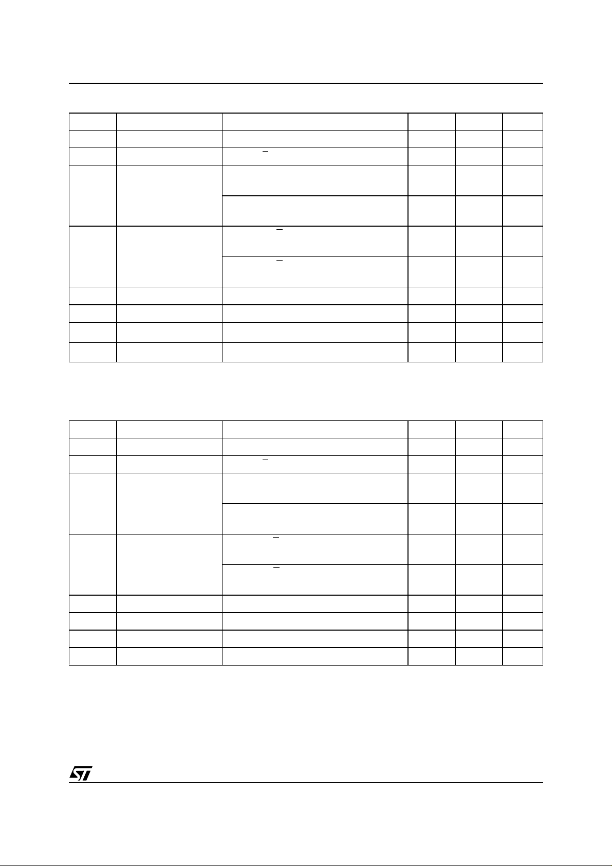
CSH
Clock Frequency D.C. 2 D.C. 5 MHz
S Active Setup Time 200 90 ns
S Not Active Setup Time 200 90 ns
S Deselect Time 200 100 ns
CS
S Active Hold Time 200 90 ns
S Not Active Hold Time 200 90 ns
t
CLH
t
CLL
2
t
2
t
t
DSU
t
Clock High Time 200 90 ns
Clock Low Time 200 90 ns
Clock Rise Time 1 1 µs
RC
Clock Fall Time 1 1 µs
FC
Data In Setup Time 40 20 ns
Data In Hold Time 50 30 ns
DH
Clock Low Hold Time after HOLD not Active 140 70 ns
Clock Low Hold Time after HOLD Active 90 40 ns
Clock High Set-up Time before HOLD Active
Clock High Set-up Time before HOLD not
Active
2
t
DIS
t
2
t
2
t
t
2
t
t
WC
Output Disable Time 250 100 ns
t
Clock Low to Output Valid 150 60 ns
V
Output Hold Time 0 0 ns
HO
Output Rise Time 100 50 ns
RO
Output Fall Time 100 50 ns
FO
HOLD High to Output Valid 100 50 ns
LZ
HOLD Low to Output High-Z 250 100 ns
HZ
Write Time 10 5 ms
Min.
t
t
CH
CH
3
Max.3Min.4Max.
60 ns
60 ns
4
Unit
28/37

M95040, M95020, M95010
Table 22. AC Characteristics (M950x0-R)
Test conditions specified in Table 11. and Table 10.
Symbol Alt. Parameter Min. Max. Unit
f
C
t
SLCH
t
SHCH
t
SHSL
t
CHSH
t
CHSL
1
t
CH
1
t
CL
2
t
CLCH
2
t
CHCL
t
DVCH
t
CHDX
t
HHCH
t
HLCH
t
CHHL
t
CHHH
2
t
SHQZ
t
CLQV
t
CLQX
2
t
QLQH
2
t
QHQL
t
HHQV
2
t
HLQZ
t
W
Note: 1. tCH + tCL must never be less than the shortest p ossible clock period, 1 / fC(max)
2. Val ue guaranteed by charact erization, not 100% tes ted in product i on.
3. Prel i m i nary data: Pr oduct under development. Please co ntact your nearest ST sales office for in f ormation .
f
SCK
t
CSS1
t
CSS2
t
CS
t
CSH
t
CLH
t
CLL
t
RC
t
FC
t
DSU
t
DH
t
DIS
t
t
HO
t
RO
t
FO
t
t
HZ
t
WC
LZ
Clock Frequency D.C. 2 MHz
S Active Setup Time 200 ns
S Not Active Setup Time 200 ns
S Deselect Time 200 ns
S Active Hold Time 200 ns
S Not Active Hold Time 200 ns
Clock High Time 200 ns
Clock Low Time 200 ns
Clock Rise Time 1 µs
Clock Fall Time 1 µs
Data In Setup Time 40 ns
Data In Hold Time 50 ns
Clock Low Hold Time after HOLD not Active 140 ns
Clock Low Hold Time after HOLD Active 90 ns
Clock High Set-up Time before HOLD Active 120 ns
Clock High Set-up Time before HOLD not Active 120 ns
Output Disable Time 250 ns
V
Clock Low to Output Valid 180 ns
Output Hold Time 0 ns
Output Rise Time 100 ns
Output Fall Time 100 ns
HOLD High to Output Valid 100 ns
HOLD Low to Output High-Z 250 ns
Write Time 10 ms
29/37

M95040, M95020, M95010
Figure 16. Se ri al Input Timing
S
C
tDVCH
tSLCH
tSHSL
tCHSHtCHSL
tSHCH
tCHCL
D
Q
Figure 17. Hol d T im i ng
S
C
Q
MSB IN
High Impedance
tCHDX
tCHHL
tCLCH
LSB IN
AI01447C
tHLCH
tHHCH
tCHHH
tHHQVtHLQZ
30/37
D
HOLD
AI02032B

Figure 18. Out put Timing
S
C
tCLQV
tCLQV
tCH
M95040, M95020, M95010
tCL
tSHQZ
tCLQX
Q
ADDR.LSB IN
D
tCLQX
LSB OUT
tQLQH
tQHQL
AI01449D
31/37

M95040, M95020, M95010
PACKAG E MECHANICAL
Figure 19. PDIP8 – 8 pin Plastic DIP, 0.25mm lead frame, Package Outline
b2
A2
A1AL
be
D
8
E1
1
Note: Drawing is not to scale.
E
c
eA
eB
PDIP-B
Table 23. PDIP8 – 8 pin Plastic DIP, 0.25mm lead frame, Package Mechanical Data
Symb.
Typ. Min. Max. Typ. Min. Max.
A 5.33 0.210
mm inches
32/37
A1 0.38 0.015
A2 3.30 2.92 4.95 0.130 0.115 0.195
b 0.46 0.36 0.56 0.018 0.014 0.022
b2 1.52 1.14 1.78 0.060 0.045 0.070
c 0.25 0.20 0.36 0.010 0.008 0.014
D 9.27 9.02 10.16 0.365 0.355 0.400
E 7.87 7.62 8.26 0.310 0.300 0.325
E1 6.35 6.10 7.11 0.250 0.240 0.280
e2.54––0.100––
eA 7.62 – – 0.300 – –
eB 10.92 0.430
L 3.30 2.92 3.81 0.130 0.115 0.150

M95040, M95020, M95010
Figure 20. SO8 narrow – 8 lead Plastic Small Outline, 150 mils body width, Package Outline
h x 45˚
Note: Drawing is not to scale.
B
SO-a
A
e
D
N
1
CP
E
H
C
LA1 α
Table 24. SO8 narrow – 8 lead Plastic Small Outline, 150 mils body width, Package Mechanical Data
Symb.
Typ. Min. Max. Typ. Min. Max.
A 1.35 1.75 0.053 0.069
A1 0.10 0.25 0.004 0.010
B 0.33 0.51 0.013 0.020
mm inches
C 0.19 0.25 0.007 0.010
D 4.80 5.00 0.189 0.197
E 3.80 4.00 0.150 0.157
e1.27––0.050––
H 5.80 6.20 0.228 0.244
h 0.25 0.50 0.010 0.020
L 0.40 0.90 0.016 0.035
α 0° 8° 0° 8°
N8 8
CP 0.10 0.004
33/37

M95040, M95020, M95010
Figure 21. TSSOP8 – 8 lead Thin Shrink S mall Outlin e, Packa ge Ou tline
D
8
1
CP
Note: Drawing is not to scale.
5
EE1
4
α
A2A
A1
eb
L
L1
TSSOP8AM
Table 25. TSSOP8 – 8 lead Thin Shrink Small Outline, Package Mechanical Data
Symbol
Typ. Min. Max. Typ. Min. Max.
A 1.200 0.0472
A1 0.050 0.150 0.0020 0.0059
A2 1.000 0.800 1.050 0.0394 0.0315 0.0413
mm inches
c
34/37
b 0.190 0.300 0.0075 0.0118
c 0.090 0.200 0.0035 0.0079
CP 0.100 0.0039
D 3.000 2.900 3.100 0.1181 0.1142 0.1220
e 0.650 – – 0.0256 – –
E 6.400 6.200 6.600 0.2520 0.2441 0.2598
E1 4.400 4.300 4.500 0.1732 0.1693 0.1772
L 0.600 0.450 0.750 0.0236 0.0177 0.0295
L1 1.000 0.0394
α 0° 8° 0° 8°

M95040, M95020, M95010
PART NUMBERING
Table 26. Ordering Information Scheme
Example: M95040 – W MN 6 T P /W
Device Type
M95 = SPI serial access EEPROM
Device Function
040 = 4 Kbit (512 x 8)
020 = 2 Kbit (256 x 8)
010 = 1 Kbit (128 x 8)
Operating Voltage
blank = V
W = V
R = V
Package
BN = PDIP8
MN = SO8 (150 mil width)
DW = TSSOP8 (169 mil width)
= 4.5 to 5.5V
CC
= 2.5 to 5.5V
CC
= 1.8 to 5.5V
CC
Device Grade
6 = Industrial temperature range, –40 to 85 °C.
Device tested with standard test flow
3 = Device tested with High Reliability Certified Flow
1
.
Automotive temperature range (–40 to 125 °C)
Option
blank = Standard Packing
T = Tape and Reel Packing
Plating Technology
blank = Standard SnPb plating
P = Lead-Free and RoHS compliant
G = Lead-Free, RoHS compliant, Sb
Process
2
-free and TBBA-free
2O3
blank = F6SP20%
/W = F6SP36%
Note: 1. ST strongly recommends the use of the Automotive Grade devices for use in an automotive environment. The High Reliability Cer-
For a list of available options (speed, package,
etc.) or for further information on any aspect of this
tified Flow (HRCF) is described in the quality not e QNEE9801. Please ask your neares t S T sales office for a copy.
2. Used only for Device Grade 3
device, please contact your nearest ST Sales Office.
Table 27. How to Identify Present and Previous Products by the Process Identification Letter
Markings on Present Products
95040W6
AYWWW (or AYWWG)
1
Markings on Previous Products
95040W6
AYWWK
1
35/37

M95040, M95020, M95010
REVISION HISTORY
Table 28. Document Revision History
Date Version Description of Revision
10-May-2000 2.2 s/issuing three bytes/issuing two bytes/ in the 2nd sentence of the Byte Write Operation
Human Body Model meets JEDEC std (Table 2). Minor adjustments to Figs 7,9,10,11 & Tab
16-Mar-2001 2.3
19-Jul-2001 2.4 Temperature range ‘3’ added to the -W supply voltage range in DC and AC characteristics
11-Oct-2001 3.0 Document reformatted using the new template
26-Feb-2002 3.1 Description of chip deselect after 8th clock pulse made more explicit
9. Wording changes, according to the standard glossary
Illustrations and Package Mechanical data updated
27-Sep-2002 3.2
Position of A8 in Read Instruction Sequence Figure corrected. Load Capacitance C
changed
24-Oct-2002 3.3 Minimum values for tCHHL and tCHHH changed.
24-Feb-2003 3.4 Description of Read from Memory Array (READ) instruction corrected, and clarified
28-May-2003 3.5 New products, identified by the process letter W, added
Correction to current products, identified by the process letter K not L.
25-Jun-2003 3.6
changed in DC characteristics, and t
CC
Voltage range -S upgraded by removing it, and adding the -R voltage range in its place
CHHL
, t
substituted in AC characteristics
CHHH
I
Temperature range 5 removed.
21-Nov-2003 4.0
02-Feb-2004 4.1
01-Mar-2004 5.0
Table of contents, and Pb-free options added. V
V
(max) and t
IL
Absolute Maximum Ratings for V
(max) changed
CLQV
(min) and VCC(min) improved. Soldering temperature
IO
information clarified for RoHS compliant devices. New 5V and 2.5V devices, with process
letter W, promoted from preliminary data to full data. Device Grade 3 clarified, with reference
(min) improved to -0.45V
IL
to HRCF and automotive environments
Product List summary table added. Process identification letter “G” information added. Order
05-Oct-2004 6.0
information for Tape and Reel changed to T. AEC-Q100-002 compliance. Device Grade
informaton clarified. tHHQX corrected to tHHQV. Signal Description updated.
10MHz, 5ms Write is now the present product. tCH+tCL<1/fC constraint clarified
L
36/37

M95040, M95020, M95010
Information furnished is believed to be accurate and reliable. However, STMicroelectronics a ssumes no responsibility for the consequences
of use of such information nor for any infringement of patents or other rights of third parties which may result from its use. No license is granted
by implication or otherwise under any patent or patent rights of STMicroelectronics. Specifications mentioned in this publication are sub j e c t
to change without notice. This publication supersedes and replaces all information previously supplied. STMicroelectronics products are not
authori zed for use as crit i cal compon ents in life support devic es or systems without express writt en approval of STMicroel ectronics.
The ST logo is a registered trademark of STMicroel ectronics.
All other nam es are the pro perty of their respectiv e owners
© 2004 STMi croelectro n ics - All righ ts reserved
Australi a - Belgium - B razil - Canada - China - Czech Republi c - Finland - F rance - Germ any - Hong Ko ng - I n dia - Israel - It al y - Japan -
Malaysia - M al ta - Morocco - Singapore - Spain - Sweden - Swit zerland - Un i ted Kingdom - United Sta tes of Americ a
STMicroelectron ics group of com panies
www.st.com
37/37
 Loading...