

ST M93C86-125, M93C76-125, M93C66-125, M93C56-125, M93C46-125 User Manual
M93C86-125 M93C76-125 M93C66-125
PDIP8 (BN)
SO8 (MN)
150 mil width
TSSOP8 (DW)
169 mil width
M93C56-125 M93C46-125
Automotive 16-Kbit, 8-Kbit, 4-Kbit, 2-Kbit and 1-Kbit
(8-bit or 16-bit wide) MICROWIRE serial EEPROM
Datasheet − production data
Features
■ Industry standard MICROWIRE
■ Memory array: 1 Kb, 2Kb, 4Kb, 8 Kb or 16 Kb
■ Dual organization: by word (x16) or byte (x8)
■ Write
– Byte within 5 ms
– Word within 5 ms
■ READY/BUSY signal during programming
■ 2 MHz clock rate
■ Sequential read operation
■ Single supply voltage: 4.5 V to 5.5 V or 2.5 V
to 5.5 V
■ Operating temperature range: -40°c up to
125°C
■ Enhanced ESD protection
■ More than 1 million Write cycles
■ More than 40-year data retention
■ Packages
– SO8, TSSOP8 packages: RoHS-compliant
and Halogen-free (ECOPACK2
– PDIP8 package: RoHS-compliant
(ECOPACK1
®
)
TM
bus
®
)
March 2012 Doc ID 022572 Rev 1 1/32
This is information on a product in full production.
www.st.com
1

Contents M93C86-125 M93C76-125 M93C66-125 M93C56-125 M93C46-125
Contents
1 Description . . . . . . . . . . . . . . . . . . . . . . . . . . . . . . . . . . . . . . . . . . . . . . . . . 6
2 Connecting to the serial bus . . . . . . . . . . . . . . . . . . . . . . . . . . . . . . . . . . 9
3 Operating features . . . . . . . . . . . . . . . . . . . . . . . . . . . . . . . . . . . . . . . . . 10
3.1 Supply voltage (VCC) . . . . . . . . . . . . . . . . . . . . . . . . . . . . . . . . . . . . . . . . 10
3.1.1 Operating supply voltage (VCC) . . . . . . . . . . . . . . . . . . . . . . . . . . . . . . . 10
3.1.2 Power-up conditions . . . . . . . . . . . . . . . . . . . . . . . . . . . . . . . . . . . . . . . 10
3.1.3 Power-up and device reset . . . . . . . . . . . . . . . . . . . . . . . . . . . . . . . . . . 10
3.1.4 Power-down . . . . . . . . . . . . . . . . . . . . . . . . . . . . . . . . . . . . . . . . . . . . . . 10
4 Memory organization . . . . . . . . . . . . . . . . . . . . . . . . . . . . . . . . . . . . . . . 11
5 Instructions . . . . . . . . . . . . . . . . . . . . . . . . . . . . . . . . . . . . . . . . . . . . . . . 12
5.1 Read Data from Memory . . . . . . . . . . . . . . . . . . . . . . . . . . . . . . . . . . . . . 14
5.2 Write Enable and Write Disable . . . . . . . . . . . . . . . . . . . . . . . . . . . . . . . . 14
5.3 Erase Byte or Word . . . . . . . . . . . . . . . . . . . . . . . . . . . . . . . . . . . . . . . . . 15
5.4 Write . . . . . . . . . . . . . . . . . . . . . . . . . . . . . . . . . . . . . . . . . . . . . . . . . . . . . 16
5.5 Erase All . . . . . . . . . . . . . . . . . . . . . . . . . . . . . . . . . . . . . . . . . . . . . . . . . . 16
5.6 Write All . . . . . . . . . . . . . . . . . . . . . . . . . . . . . . . . . . . . . . . . . . . . . . . . . . 17
6 READY/BUSY status . . . . . . . . . . . . . . . . . . . . . . . . . . . . . . . . . . . . . . . . 18
7 Initial delivery state . . . . . . . . . . . . . . . . . . . . . . . . . . . . . . . . . . . . . . . . . 18
8 Common I/O operation . . . . . . . . . . . . . . . . . . . . . . . . . . . . . . . . . . . . . . 18
9 Clock pulse counter . . . . . . . . . . . . . . . . . . . . . . . . . . . . . . . . . . . . . . . . 19
10 Maximum rating . . . . . . . . . . . . . . . . . . . . . . . . . . . . . . . . . . . . . . . . . . . . 20
11 DC and AC parameters . . . . . . . . . . . . . . . . . . . . . . . . . . . . . . . . . . . . . . 21
12 Package mechanical data . . . . . . . . . . . . . . . . . . . . . . . . . . . . . . . . . . . . 27
2/32 Doc ID 022572 Rev 1

M93C86-125 M93C76-125 M93C66-125 M93C56-125 M93C46-125 Contents
13 Part numbering . . . . . . . . . . . . . . . . . . . . . . . . . . . . . . . . . . . . . . . . . . . . 30
14 Revision history . . . . . . . . . . . . . . . . . . . . . . . . . . . . . . . . . . . . . . . . . . . 31
Doc ID 022572 Rev 1 3/32

List of tables M93C86-125 M93C76-125 M93C66-125 M93C56-125 M93C46-125
List of tables
Table 1. Memory size versus organization . . . . . . . . . . . . . . . . . . . . . . . . . . . . . . . . . . . . . . . . . . . . . 6
Table 2. Signal names . . . . . . . . . . . . . . . . . . . . . . . . . . . . . . . . . . . . . . . . . . . . . . . . . . . . . . . . . . . . 7
Table 3. Instruction set for the M93Cx6 . . . . . . . . . . . . . . . . . . . . . . . . . . . . . . . . . . . . . . . . . . . . . . . 7
Table 4. Instruction set for the M93C46 . . . . . . . . . . . . . . . . . . . . . . . . . . . . . . . . . . . . . . . . . . . . . . 12
Table 5. Instruction set for the M93C56 and M93C66 . . . . . . . . . . . . . . . . . . . . . . . . . . . . . . . . . . . 13
Table 6. Instruction set for the M93C76 and M93C86 . . . . . . . . . . . . . . . . . . . . . . . . . . . . . . . . . . . 13
Table 7. Absolute maximum ratings . . . . . . . . . . . . . . . . . . . . . . . . . . . . . . . . . . . . . . . . . . . . . . . . . 20
Table 8. Operating conditions (M93Cx6) . . . . . . . . . . . . . . . . . . . . . . . . . . . . . . . . . . . . . . . . . . . . . 21
Table 9. Operating conditions (M93Cx6-W) . . . . . . . . . . . . . . . . . . . . . . . . . . . . . . . . . . . . . . . . . . . 21
Table 10. AC measurement conditions (M93Cx6) . . . . . . . . . . . . . . . . . . . . . . . . . . . . . . . . . . . . . . . 21
Table 11. AC measurement conditions (M93Cx6-W) . . . . . . . . . . . . . . . . . . . . . . . . . . . . . . . . . . . . . 21
Table 12. Capacitance . . . . . . . . . . . . . . . . . . . . . . . . . . . . . . . . . . . . . . . . . . . . . . . . . . . . . . . . . . . . 22
Table 13. DC characteristics (M93Cx6, device grade 3) . . . . . . . . . . . . . . . . . . . . . . . . . . . . . . . . . . 22
Table 14. DC characteristics (M93Cx6-W, device grade 3) . . . . . . . . . . . . . . . . . . . . . . . . . . . . . . . . 23
Table 15. AC characteristics (M93Cx6, device grade 3). . . . . . . . . . . . . . . . . . . . . . . . . . . . . . . . . . . 24
Table 16. AC characteristics (M93Cx6-W, device grade 3) . . . . . . . . . . . . . . . . . . . . . . . . . . . . . . . . 25
Table 17. PDIP8 – 8 lead plastic dual in-line package, 300 mils body width, package
mechanical data . . . . . . . . . . . . . . . . . . . . . . . . . . . . . . . . . . . . . . . . . . . . . . . . . . . . . . . . . 27
Table 18. SO8 narrow – 8 lead plastic small outline, 150 mils body width, package data . . . . . . . . . 28
Table 19. TSSOP8 – 8 lead thin shrink small outline, package mechanical data . . . . . . . . . . . . . . . . 29
Table 20. Ordering information scheme . . . . . . . . . . . . . . . . . . . . . . . . . . . . . . . . . . . . . . . . . . . . . . . 30
Table 21. Document revision history . . . . . . . . . . . . . . . . . . . . . . . . . . . . . . . . . . . . . . . . . . . . . . . . . 31
4/32 Doc ID 022572 Rev 1

M93C86-125 M93C76-125 M93C66-125 M93C56-125 M93C46-125 List of figures
List of figures
Figure 1. Logic diagram . . . . . . . . . . . . . . . . . . . . . . . . . . . . . . . . . . . . . . . . . . . . . . . . . . . . . . . . . . . . 6
Figure 2. DIP, SO and TSSOP connections (top view) . . . . . . . . . . . . . . . . . . . . . . . . . . . . . . . . . . . . 8
Figure 3. Bus master and memory devices on the serial bus . . . . . . . . . . . . . . . . . . . . . . . . . . . . . . . 9
Figure 4. READ, WRITE, WEN, WDS sequences . . . . . . . . . . . . . . . . . . . . . . . . . . . . . . . . . . . . . . . 15
Figure 5. ERASE, ERAL sequences . . . . . . . . . . . . . . . . . . . . . . . . . . . . . . . . . . . . . . . . . . . . . . . . . 16
Figure 6. WRAL sequence . . . . . . . . . . . . . . . . . . . . . . . . . . . . . . . . . . . . . . . . . . . . . . . . . . . . . . . . . 17
Figure 7. Write sequence with one clock glitch . . . . . . . . . . . . . . . . . . . . . . . . . . . . . . . . . . . . . . . . . 19
Figure 8. AC testing input output waveforms . . . . . . . . . . . . . . . . . . . . . . . . . . . . . . . . . . . . . . . . . . . 22
Figure 9. Synchronous timing (start and op-code input) . . . . . . . . . . . . . . . . . . . . . . . . . . . . . . . . . . 26
Figure 10. Synchronous timing (Read or Write). . . . . . . . . . . . . . . . . . . . . . . . . . . . . . . . . . . . . . . . . . 26
Figure 11. Synchronous timing (Read or Write). . . . . . . . . . . . . . . . . . . . . . . . . . . . . . . . . . . . . . . . . . 26
Figure 12. PDIP8 – 8 lead plastic dual in-line package, 300 mils body width, package
outline . . . . . . . . . . . . . . . . . . . . . . . . . . . . . . . . . . . . . . . . . . . . . . . . . . . . . . . . . . . . . . . . . 27
Figure 13. SO8 narrow – 8 lead plastic small outline, 150 mils body width, package outline . . . . . . . 28
Figure 14. TSSOP8 – 8 lead thin shrink small outline, package outline . . . . . . . . . . . . . . . . . . . . . . . 29
Doc ID 022572 Rev 1 5/32
Description M93C86-125 M93C76-125 M93C66-125 M93C56-125 M93C46-125
AI01928
D
V
CC
M93Cx6
V
SS
C
Q
S
ORG
1 Description
The M93C46 (1 Kbit), M93C56 (2 Kbit), M93C66 (4 Kbit), M93C76 (8 Kbit) and M93C86
(16 Kbit) are Electrically Erasable PROgrammable Memory (EEPROM) devices accessed
through the MICROWIRE bus protocol. The memory array can be configured either in bytes
(x8b) or in words (x16b).
The M93Cx6 devices operate within a voltage supply range from 4.5 V to 5.5 V, and the
M93Cx6-W devices operate within a voltage supply range from 2.5 V to 5.5 V.
The M93Cx6 devices are guaranteed over the -40°C/+125°C temperature range and are
compliant with the Automotive standard AEC-Q100 Grade 1.
Table 1. Memory size versus organization
Device Number of bits Number of 8-bit bytes Number of 16-bit words
M93C86 16384 2048 1024
M93C76 8192 1024 512
M93C66 4096 512 256
M93C56 2048 256 128
M93C46 1024 128 64
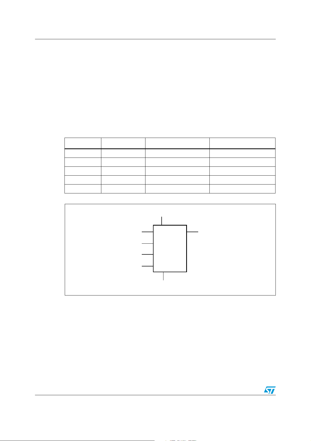
Figure 1. Logic diagram
6/32 Doc ID 022572 Rev 1
M93C86-125 M93C76-125 M93C66-125 M93C56-125 M93C46-125 Description
Table 2. Signal names
Signal name Function Direction
S Chip Select Input
D Serial Data input Input
Q Serial Data output Output
C Serial Clock Input
ORG Organization Select Input
V
CC
V
SS
Supply voltage
Ground
The M93Cx6 is accessed by a set of instructions, as summarized in Ta bl e 3 , and in more
detail in Table 4: Instruction set for the M93C46 to Table 6: Instruction set for the M93C76
and M93C86).
Table 3. Instruction set for the M93Cx6
Instruction Description Data
READ Read Data from Memory Byte or Word
WRITE Write Data to Memory Byte or Word
WEN Write Enable
WDS Write Disable
ERASE Erase Byte or Word Byte or Word
ERAL Erase All Memory
WRAL Write All Memory with same Data
A Read Data from Memory (READ) instruction loads the address of the first byte or word to
be read in an internal address register. The data at this address is then clocked out serially.
The address register is automatically incremented after the data is output and, if Chip Select
Input (S) is held High, the M93Cx6 can output a sequential stream of data bytes or words. In
this way, the memory can be read as a data stream from eight to 16384 bits long (in the
case of the M93C86), or continuously (the address counter automatically rolls over to 00h
when the highest address is reached).
Programming is internally self-timed (the external clock signal on Serial Clock (C) may be
stopped or left running after the start of a Write cycle) and does not require an Erase cycle
prior to the Write instruction. The Write instruction writes 8 or 16 bits at a time into one of the
byte or word locations of the M93Cx6. After the start of the programming cycle, a
Busy/Ready signal is available on Serial Data Output (Q) when Chip Select Input (S) is
driven High.
An internal Power-on Data Protection mechanism in the M93Cx6 inhibits the device when
the supply is too low.
Doc ID 022572 Rev 1 7/32

Description M93C86-125 M93C76-125 M93C66-125 M93C56-125 M93C46-125
V
SS
Q
ORG
DUC
SV
CC
D
AI01929B
M93Cx6
1
2
3
4
8
7
6
5
Figure 2. DIP, SO and TSSOP connections (top view)
1. See Section 12: Package mechanical data for package dimensions, and how to identify pin-1.
2. DU = Don’t Use. The DU (do not use) pin does not contribute to the normal operation of the device. It is
reserved for use by STMicroelectronics during test sequences. The pin may be left unconnected or may be
connected to V
or VSS.
CC
8/32 Doc ID 022572 Rev 1
M93C86-125 M93C76-125 M93C66-125 M93C56-125 M93C46-125 Connecting to the serial bus
AI14377b
Bus master
M93xxx
memory device
SDO
SDI
SCK
CQD
S
M93xxx
memory device
CQD
S
M93xxx
memory device
CQD
S
CS3 CS2 CS1
ORG
ORG
ORG
RR R
V
CC
V
CC
V
CC
V
CC
V
SS
V
SS
V
SS
V
SS
R
2 Connecting to the serial bus
Figure 3 shows an example of three memory devices connected to an MCU, on a serial bus.
Only one device is selected at a time, so only one device drives the Serial Data output (Q)
line at a time, the other devices are high impedance.
The pull-down resistor R (represented in Figure 3) ensures that no device is selected if the
bus master leaves the S line in the high impedance state.
In applications where the bus master may be in a state where all inputs/outputs are high
impedance at the same time (for example, if the bus master is reset during the transmission
of an instruction), the clock line (C) must be connected to an external pull-down resistor so
that, if all inputs/outputs become high impedance, the C line is pulled low (while the S line is
pulled low): this ensures that C does not become high at the same time as S goes low, and
so, that the t
Figure 3. Bus master and memory devices on the serial bus
requirement is met. The typical value of R is 100 kΩ.
SLCH
Doc ID 022572 Rev 1 9/32

Operating features M93C86-125 M93C76-125 M93C66-125 M93C56-125 M93C46-125
3 Operating features
3.1 Supply voltage (VCC)
3.1.1 Operating supply voltage (VCC)
Prior to selecting the memory and issuing instructions to it, a valid and stable VCC voltage
within the specified [V
DC supply voltage, it is recommended to decouple the V
(usually of the order of 10 nF to 100 nF) close to the V
This voltage must remain stable and valid until the end of the transmission of the instruction
and, for a Write instruction, until the completion of the internal write cycle (t
3.1.2 Power-up conditions
When the power supply is turned on, VCC rises from VSS to VCC. During this time, the Chip
Select (S) line is not allowed to float and should be driven to V
recommended to connect the S line to V
The V
rise time must not vary faster than 1 V/µs.
CC
(min), VCC(max)] range must be applied. In order to secure a stable
CC
via a suitable pull-down resistor.
SS
line with a suitable capacitor
CC
CC/VSS
package pins.
, it is therefore
SS
).
W
3.1.3 Power-up and device reset
In order to prevent inadvertent Write operations during power-up, a power on reset (POR)
circuit is included. At power-up (continuous rise of V
instruction until V
lower than the minimum V
has reached the power on reset threshold voltage (this threshold is
CC
operating voltage defined in Operating conditions, in
CC
Section 11: DC and AC parameters).
When V
● Standby Power mode
● deselected (assuming that there is a pull-down resistor on the S line)
passes the POR threshold, the device is reset and is in the following state:
CC
3.1.4 Power-down
At power-down (continuous decrease in VCC), as soon as VCC drops from the normal
operating voltage to below the power on reset threshold voltage, the device stops
responding to any instruction sent to it.
During power-down, the device must be deselected and in the Standby Power mode (that is,
there should be no internal Write cycle in progress).
), the device does not respond to any
CC
10/32 Doc ID 022572 Rev 1
 Loading...