

查询M9306-BN3T供应商
16Kbit, 8Kbit, 4Kbit, 2Kbit and 1Kbit (8-bit or 16-bit wide)
MICROWIRE® Serial Access EEPROM
FEATURES SUMMARY
■ Industry Standard MICROWIRE Bus
■ Single Supply Voltage:
– 4.5 to 5.5V for M93Cx6
– 2.5 to 5.5V for M93Cx6-W
– 1.8 to 5.5V for M93Cx6-R
■ Dual Organization: by Word (x16) or Byte (x8)
■ Programming Instructions that work on: Byte,
Word or Entire Memory
■ Self-timed Programming Cycle with Auto-
Erase
■ Ready/Busy Signal During Programming
■ Speed:
– 1MHz Clock Rate, 10ms Write Time
(Current product, identified by process
identification letter F or M)
– 2MHz Clock Rate, 5ms Write Time (New
Product, identified by process
identification letter W or G or S)
■ Sequential Read Operation
■ Enhanced ESD/Latch-Up Behaviour
■ More than 1 Million Erase/Write Cycles
■ More than 40 Year Data Retention
M93C86, M93C76, M93C66
M93C56, M93C46
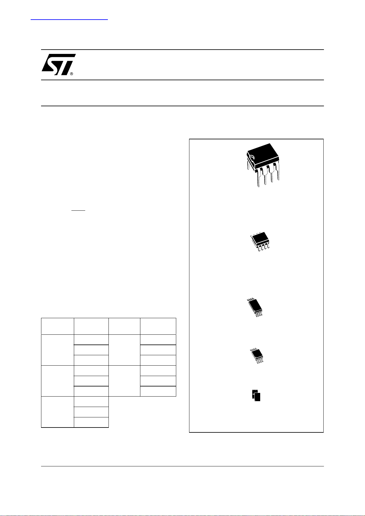
Figure 1. Packages
8
1
PDIP8 (BN)
8
1
SO8 (MN)
150 mil width
Table 1. Product List
Reference
M93C86
M93C76
M93C66
Part
Number
M93C86
M93C86-W M93C56-W
M93C86-R M93C56-R
M93C76
M93C76-W M93C46-W
M93C76-R M93C46-R
M93C66
M93C66-W
M93C66-R
Reference
M93C56
M93C46
Part
Number
M93C56
M93C46
TSSOP8 (DW)
169 mil width
TSSOP8 (DS)
3x3mm² body size (MSOP)
UFDFPN8 (MB)
2x3mm² (MLP)
1/31August 2004

M93C86, M93C76, M93C66, M93C56, M93C46
TABLE OF CONTENTS
FEATURES SUMMARY . . . . . . . . . . . . . . . . . . . . . . . . . . . . . . . . . . . . . . . . . . . . . . . . . . . . . . . . . . . . . 1
Table 1. Product List . . . . . . . . . . . . . . . . . . . . . . . . . . . . . . . . . . . . . . . . . . . . . . . . . . . . . . . . . . . . 1
Figure 1. Packages. . . . . . . . . . . . . . . . . . . . . . . . . . . . . . . . . . . . . . . . . . . . . . . . . . . . . . . . . . . . . . 1
Figure 2. Logic Diagram . . . . . . . . . . . . . . . . . . . . . . . . . . . . . . . . . . . . . . . . . . . . . . . . . . . . . . . . . . 4
Table 2. Signal Names . . . . . . . . . . . . . . . . . . . . . . . . . . . . . . . . . . . . . . . . . . . . . . . . . . . . . . . . . . 4
Table 3. Memory Size versus Organization. . . . . . . . . . . . . . . . . . . . . . . . . . . . . . . . . . . . . . . . . . . 4
Table 4. Instruction Set for the M93Cx6 . . . . . . . . . . . . . . . . . . . . . . . . . . . . . . . . . . . . . . . . . . . . .4
Figure 3. DIP, SO, TSSOP and MLP Connections (Top View). . . . . . . . . . . . . . . . . . . . . . . . . . . . . 5
MEMORY ORGANIZATION . . . . . . . . . . . . . . . . . . . . . . . . . . . . . . . . . . . . . . . . . . . . . . . . . . . . . . . . . . 5
POWER-ON DATA PROTECTION . . . . . . . . . . . . . . . . . . . . . . . . . . . . . . . . . . . . . . . . . . . . . . . . . . . . .5
INSTRUCTIONS . . . . . . . . . . . . . . . . . . . . . . . . . . . . . . . . . . . . . . . . . . . . . . . . . . . . . . . . . . . . . . . . . . . 6
Table 5. Instruction Set for the M93C46 . . . . . . . . . . . . . . . . . . . . . . . . . . . . . . . . . . . . . . . . . . . . .6
Table 6. Instruction Set for the M93C56 and M93C66 . . . . . . . . . . . . . . . . . . . . . . . . . . . . . . . . . . 7
Table 7. Instruction Set for the M93C76 and M93C86 . . . . . . . . . . . . . . . . . . . . . . . . . . . . . . . . . . 7
Read . . . . . . . . . . . . . . . . . . . . . . . . . . . . . . . . . . . . . . . . . . . . . . . . . . . . . . . . . . . . . . . . . . . . . . . . . 8
Erase/Write Enable and Disable. . . . . . . . . . . . . . . . . . . . . . . . . . . . . . . . . . . . . . . . . . . . . . . . . . . 8
Figure 4. READ, WRITE, EWEN, EWDS Sequences. . . . . . . . . . . . . . . . . . . . . . . . . . . . . . . . . . . . 8
Erase. . . . . . . . . . . . . . . . . . . . . . . . . . . . . . . . . . . . . . . . . . . . . . . . . . . . . . . . . . . . . . . . . . . . . . . . . 9
Write . . . . . . . . . . . . . . . . . . . . . . . . . . . . . . . . . . . . . . . . . . . . . . . . . . . . . . . . . . . . . . . . . . . . . . . . . 9
Figure 5. ERASE, ERAL Sequences . . . . . . . . . . . . . . . . . . . . . . . . . . . . . . . . . . . . . . . . . . . . . . . . 9
Erase All. . . . . . . . . . . . . . . . . . . . . . . . . . . . . . . . . . . . . . . . . . . . . . . . . . . . . . . . . . . . . . . . . . . . . 10
Write All . . . . . . . . . . . . . . . . . . . . . . . . . . . . . . . . . . . . . . . . . . . . . . . . . . . . . . . . . . . . . . . . . . . . . 10
Figure 6. WRAL Sequence . . . . . . . . . . . . . . . . . . . . . . . . . . . . . . . . . . . . . . . . . . . . . . . . . . . . . . . 10
READY/BUSY STATUS . . . . . . . . . . . . . . . . . . . . . . . . . . . . . . . . . . . . . . . . . . . . . . . . . . . . . . . . . . . . 11
COMMON I/O OPERATION . . . . . . . . . . . . . . . . . . . . . . . . . . . . . . . . . . . . . . . . . . . . . . . . . . . . . . . . . 11
CLOCK PULSE COUNTER . . . . . . . . . . . . . . . . . . . . . . . . . . . . . . . . . . . . . . . . . . . . . . . . . . . . . . . . . 11
Figure 7. Write Sequence with One Clock Glitch . . . . . . . . . . . . . . . . . . . . . . . . . . . . . . . . . . . . . . 11
MAXIMUM RATING. . . . . . . . . . . . . . . . . . . . . . . . . . . . . . . . . . . . . . . . . . . . . . . . . . . . . . . . . . . . . . . . 12
Table 8. Absolute Maximum Ratings. . . . . . . . . . . . . . . . . . . . . . . . . . . . . . . . . . . . . . . . . . . . . . . 12
DC AND AC PARAMETERS. . . . . . . . . . . . . . . . . . . . . . . . . . . . . . . . . . . . . . . . . . . . . . . . . . . . . . . . . 13
Table 9. Operating Conditions (M93Cx6) . . . . . . . . . . . . . . . . . . . . . . . . . . . . . . . . . . . . . . . . . . . 13
Table 10. Operating Conditions (M93Cx6-W) . . . . . . . . . . . . . . . . . . . . . . . . . . . . . . . . . . . . . . . . . 13
Table 11. Operating Conditions (M93Cx6-R) . . . . . . . . . . . . . . . . . . . . . . . . . . . . . . . . . . . . . . . . . 13
Table 12. AC Measurement Conditions (M93Cx6) . . . . . . . . . . . . . . . . . . . . . . . . . . . . . . . . . . . . . 14
Table 13. AC Measurement Conditions (M93Cx6-W and M93Cx6-R) . . . . . . . . . . . . . . . . . . . . . . 14
Figure 8. AC Testing Input Output Waveforms. . . . . . . . . . . . . . . . . . . . . . . . . . . . . . . . . . . . . . . . 14
2/31

M93C86, M93C76, M93C66, M93C56, M93C46
Table 14. Capacitance. . . . . . . . . . . . . . . . . . . . . . . . . . . . . . . . . . . . . . . . . . . . . . . . . . . . . . . . . . . 14
Table 15. DC Characteristics (M93Cx6, Device Grade 6). . . . . . . . . . . . . . . . . . . . . . . . . . . . . . . . 15
Table 16. DC Characteristics (M93Cx6, Device Grade 7 or 3) . . . . . . . . . . . . . . . . . . . . . . . . . . . . 15
Table 17. DC Characteristics (M93Cx6-W, Device Grade 6) . . . . . . . . . . . . . . . . . . . . . . . . . . . . . 16
Table 18. DC Characteristics (M93Cx6-W, Device Grade 7 or 3). . . . . . . . . . . . . . . . . . . . . . . . . . 17
Table 19. DC Characteristics (M93Cx6-R) . . . . . . . . . . . . . . . . . . . . . . . . . . . . . . . . . . . . . . . . . . . 17
Table 20. AC Characteristics (M93Cx6, Device Grade 6, 7 or 3) . . . . . . . . . . . . . . . . . . . . . . . . . . 18
Table 21. AC Characteristics (M93Cx6-W, Device Grade 6). . . . . . . . . . . . . . . . . . . . . . . . . . . . . . 19
Table 22. AC Characteristics (M93Cx6-W, Device Grade 7 or 3) . . . . . . . . . . . . . . . . . . . . . . . . . . 20
Table 23. AC Characteristics (M93Cx6-R) . . . . . . . . . . . . . . . . . . . . . . . . . . . . . . . . . . . . . . . . . . . 21
Figure 9. Synchronous Timing (Start and Op-Code Input) . . . . . . . . . . . . . . . . . . . . . . . . . . . . . . . 22
Figure 10.Synchronous Timing (Read or Write) . . . . . . . . . . . . . . . . . . . . . . . . . . . . . . . . . . . . . . . 22
Figure 11.Synchronous Timing (Read or Write) . . . . . . . . . . . . . . . . . . . . . . . . . . . . . . . . . . . . . . . 22
PACKAGE MECHANICAL . . . . . . . . . . . . . . . . . . . . . . . . . . . . . . . . . . . . . . . . . . . . . . . . . . . . . . . . . . 23
Figure 12.PDIP8 – 8 pin Plastic DIP, 0.25mm lead frame, Package Outline . . . . . . . . . . . . . . . . . 23
Table 24. PDIP8 – 8 pin Plastic DIP, 0.25mm lead frame, Package Mechanical Data . . . . . . . . . . 23
Figure 13.SO8 narrow – 8 lead Plastic Small Outline, 150 mils body width, Package Outline . . . . 24
Table 25. SO8 narrow – 8 lead Plastic Small Outline, 150 mils body width, Package Mechanical Data
24
Figure 14.UFDFPN8 (MLP8) 8-lead Ultra thin Fine pitch Dual Flat Package No lead 2x3mm², Outline
25
Table 26. UFDFPN8 (MLP8) 8-lead Ultra thin Fine pitch Dual Flat Package No lead 2x3mm², Data.
25
Figure 15.TSSOP8 3x3mm² – 8 lead Thin Shrink Small Outline, 3x3mm² body size, Package Outline
26
Table 27. TSSOP8 3x3mm² – 8 lead Thin Shrink Small Outline, 3x3mm² body size, Mechanical Data
26
Figure 16.TSSOP8 – 8 lead Thin Shrink Small Outline, Package Outline . . . . . . . . . . . . . . . . . . . 27
Table 28. TSSOP8 – 8 lead Thin Shrink Small Outline, Package Mechanical Data . . . . . . . . . . . . 27
PART NUMBERING . . . . . . . . . . . . . . . . . . . . . . . . . . . . . . . . . . . . . . . . . . . . . . . . . . . . . . . . . . . . . . . 28
Table 29. Ordering Information Scheme . . . . . . . . . . . . . . . . . . . . . . . . . . . . . . . . . . . . . . . . . . . . . 28
Table 30. How to Identify Current and New Products by the Process Identification Letter . . . . . . . 29
REVISION HISTORY. . . . . . . . . . . . . . . . . . . . . . . . . . . . . . . . . . . . . . . . . . . . . . . . . . . . . . . . . . . . . . . 30
Table 31. Document Revision History . . . . . . . . . . . . . . . . . . . . . . . . . . . . . . . . . . . . . . . . . . . . . . . 30
3/31

M93C86, M93C76, M93C66, M93C56, M93C46
SUMMARY DESCRIPTION
These electrically erasable programmable memory (EEPROM) devices are accessed through a Serial Data Input (D) and Serial Data Output (Q)
using the MICROWIRE bus protocol.
Figure 2. Logic Diagram
V
CC
ORG
D
C
S
M93Cx6
V
SS
Q
AI01928
Table 3. Memory Size versus Organization
Device
M93C86 16384 2048 1024
M93C76 8192 1024 512
M93C66 4096 512 256
M93C56 2048 256 128
M93C46 1024 128 64
Number
of Bits
Number
of 8-bit
Bytes
Number
of 16-bit
Words
The M93Cx6 is accessed by a set of instructions,
as summarized in Table 4., and in more detail in
Table 5. to Table 7.).
Table 4. Instruction Set for the M93Cx6
Instruction Description Data
READ Read Data from Memory Byte or Word
WRITE Write Data to Memory Byte or Word
EWEN Erase/Write Enable
EWDS Erase/Write Disable
Table 2. Signal Names
S Chip Select Input
D Serial Data Input
Q Serial Data Output
C Serial Clock
ORG Organisation Select
V
CC
V
SS
Supply Voltage
Ground
The memory array organization may be divided
into either bytes (x8) or words (x16) which may be
selected by a signal applied on Organization Select (ORG). The bit, byte and word sizes of the
memories are as shown in Table 3..
ERASE Erase Byte or Word Byte or Word
ERAL Erase All Memory
WRAL
Write All Memory
with same Data
A Read Data from Memory (READ) instruction
loads the address of the first byte or word to be
read in an internal address register. The data at
this address is then clocked out serially. The address register is automatically incremented after
the data is output and, if Chip Select Input (S) is
held High, the M93Cx6 can output a sequential
stream of data bytes or words. In this way, the
memory can be read as a data stream from eight
to 16384 bits long (in the case of the M93C86), or
continuously (the address counter automatically
rolls over to 00h when the highest address is
reached).
Programming is internally self-timed (the external
clock signal on Serial Clock (C) may be stopped or
left running after the start of a Write cycle) and
does not require an Erase cycle prior to the Write
instruction. The Write instruction writes 8 or 16 bits
at a time into one of the byte or word locations of
the M93Cx6. After the start of the programming cycle, a Busy/Ready signal is available on Serial
Data Output (Q) when Chip Select Input (S) is driven High.
4/31

M93C86, M93C76, M93C66, M93C56, M93C46
An internal Power-on Data Protection mechanism
in the M93Cx6 inhibits the device when the supply
is too low.
Figure 3. DIP, SO, TSSOP and MLP
Connections (Top View)
M93Cx6
SV
1
2
D
3
Q
4
Note: 1. See PACKAGE MECHANICAL section for package di-
mensions, and how to identify pin-1.
2. DU = Don’t Use.
8
7
6
5
AI01929B
CC
DUC
ORG
V
SS
The DU (Don’t Use) pin does not contribute to the
normal operation of the device. It is reserved for
use by STMicroelectronics during test sequences.
The pin may be left unconnected or may be connected to V
is recommended for the lowest stand-by pow-
V
SS
or VSS. Direct connection of DU to
CC
er consumption.
MEMORY ORGANIZATION
The M93Cx6 memory is organized either as bytes
(x8) or as words (x16). If Organization Select
(ORG) is left unconnected (or connected to V
CC
the x16 organization is selected; when Organization Select (ORG) is connected to Ground (V
SS
the x8 organization is selected. When the M93Cx6
is in stand-by mode, Organization Select (ORG)
should be set either to V
power consumption. Any voltage between V
or VCC for minimum
SS
SS
and VCC applied to Organization Select (ORG)
may increase the stand-by current.
POWER-ON DATA PROTECTION
To prevent data corruption and inadvertent write
operations during power-up, a Power-On Reset
(POR) circuit resets all internal programming circuitry, and sets the device in the Write Disable
mode.
– At Power-up and Power-down, the device
must not be selected (that is, Chip Select Input
(S) must be driven Low) until the supply
voltage reaches the operating value V
specified in Table 9. to Table 11..
– When V
reaches its valid level, the device is
CC
properly reset (in the Write Disable mode) and
is ready to decode and execute incoming
instructions.
For the M93Cx6 devices (5V range) the POR
threshold voltage is around 3V. For the M93Cx6W (3V range) and M93Cx6-R (2V range) the POR
threshold voltage is around 1.5V.
CC
)
)
5/31

M93C86, M93C76, M93C66, M93C56, M93C46
INSTRUCTIONS
The instruction set of the M93Cx6 devices contains seven instructions, as summarized in Table
5. to Table 7.. Each instruction consists of the fol-
lowing parts, as shown in Figure 4.:
■ Each instruction is preceded by a rising edge
on Chip Select Input (S) with Serial Clock (C)
being held Low.
■ A start bit, which is the first ‘1’ read on Serial
Data Input (D) during the rising edge of Serial
Clock (C).
■ Two op-code bits, read on Serial Data Input
(D) during the rising edge of Serial Clock (C).
(Some instructions also use the first two bits of
the address to define the op-code).
Table 5. Instruction Set for the M93C46
x8 Origination (ORG = 0) x16 Origination (ORG = 1)
Instruc
tion
Description
Start
bit
Op-
Code
Address
1
■ The address bits of the byte or word that is to
be accessed. For the M93C46, the address is
made up of 6 bits for the x16 organization or 7
bits for the x8 organization (see Table 5.). For
the M93C56 and M93C66, the address is
made up of 8 bits for the x16 organization or 9
bits for the x8 organization (see Table 6.). For
the M93C76 and M93C86, the address is
made up of 10 bits for the x16 organization or
11 bits for the x8 organization (see Table 7.).
The M93Cx6 devices are fabricated in CMOS
technology and are therefore able to run as slow
as 0 Hz (static input signals) or as fast as the maximum ratings specified in Table 20. to Table 23..
Data
Required
Clock
Cycles
Address
1
Data
Required
Clock
Cycles
READ
WRITE
EWEN Erase/Write Enable 1 00 11X XXXX 10 11 XXXX 9
EWDS Erase/Write Disable 1 00 00X XXXX 10 00 XXXX 9
ERASE Erase Byte or Word 1 11 A6-A0 10 A5-A0 9
ERAL Erase All Memory 1 00 10X XXXX 10 10 XXXX 9
WRAL
Note: 1. X = Don’t Care bit.
Read Data from
Memory
Write Data to
Memory
Write All Memory
with same Data
1 10 A6-A0 Q7-Q0 A5-A0 Q15-Q0
1 01 A6-A0 D7-D0 18 A5-A0 D15-D0 25
1 00 01X XXXX D7-D0 18 01 XXXX D15-D0 25
6/31
M93C86, M93C76, M93C66, M93C56, M93C46
Table 6. Instruction Set for the M93C56 and M93C66
x8 Origination (ORG = 0) x16 Origination (ORG = 1)
Instruc
tion
READ
WRITE
Description
Read Data from
Memory
Write Data to
Memory
EWEN Erase/Write Enable 1 00
EWDS Erase/Write Disable 1 00
ERASE Erase Byte or Word 1 11 A8-A0 12 A7-A0 11
ERAL Erase All Memory 1 00
WRAL
Note: 1. X = Don’t Care bit.
Write All Memory
with same Data
2. Address bit A8 is not decoded by the M93C56.
3. Address bit A7 is not decoded by the M93C56.
Start
bit
Op-
Code
Address
1,2
Data
Required
Clock
Address
1,3
Required
Data
Cycles
1 10 A8-A0 Q7-Q0 A7-A0 Q15-Q0
1 01 A8-A0 D7-D0 20 A7-A0 D15-D0 27
100
1 1XXX
XXXX
0 0XXX
XXXX
1 0XXX
XXXX
0 1XXX
XXXX
12
12
12
D7-D0 20
11XX
XXXX
00XX
XXXX
10XX
XXXX
01XX
XXXX
D15-D0 27
Clock
Cycles
11
11
11
Table 7. Instruction Set for the M93C76 and M93C86
x8 Origination (ORG = 0) x16 Origination (ORG = 1)
Instruc
tion
READ
WRITE
Description
Read Data from
Memory
Write Data to
Memory
EWEN Erase/Write Enable 1 00
EWDS Erase/Write Disable 1 00
ERASE Erase Byte or Word 1 11 A10-A0 14 A9-A0 13
ERAL Erase All Memory 1 00
WRAL
Note: 1. X = Don’t Care bit.
Write All Memory
with same Data
2. Address bit A10 is not decoded by the M93C76.
3. Address bit A9 is not decoded by the M93C76.
Start
bit
Op-
Code
Address
1,2
Data
Required
Clock
Address
1,3
Required
Data
Cycles
1 10 A10-A0 Q7-Q0 A9-A0 Q15-Q0
1 01 A10-A0 D7-D0 22 A9-A0 D15-D0 29
100
11X XXXX
XXXX
00X XXXX
XXXX
10X XXXX
XXXX
01X XXXX
XXXX
14
14
14
D7-D0 22
11 XXXX
XXXX
00 XXXX
XXXX
10 XXXX
XXXX
01 XXXX
XXXX
D15-D0 29
Clock
Cycles
13
13
13
7/31

M93C86, M93C76, M93C66, M93C56, M93C46
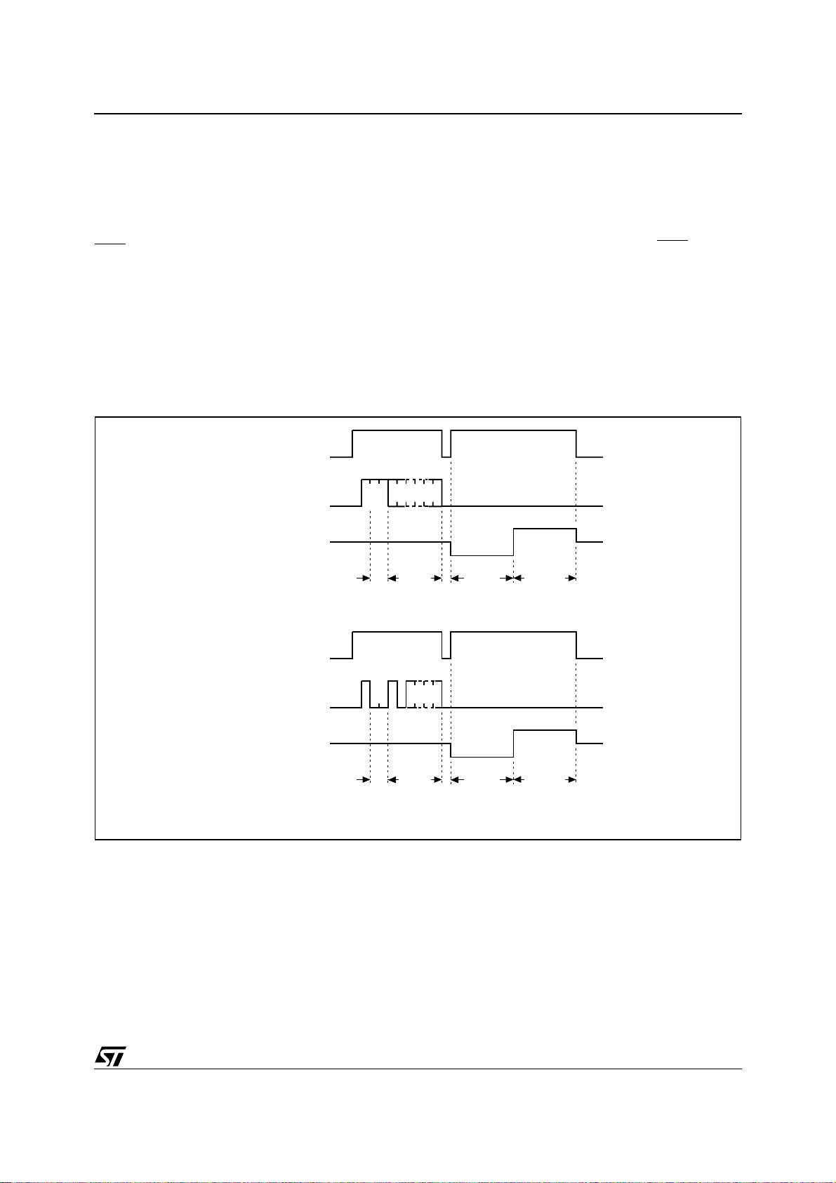
Read
The Read Data from Memory (READ) instruction
outputs data on Serial Data Output (Q). When the
instruction is received, the op-code and address
are decoded, and the data from the memory is
transferred to an output shift register. A dummy 0
bit is output first, followed by the 8-bit byte or 16bit word, with the most significant bit first. Output
data changes are triggered by the rising edge of
Serial Clock (C). The M93Cx6 automatically increments the internal address register and clocks out
the next byte (or word) as long as the Chip Select
Input (S) is held High. In this case, the dummy 0 bit
is not output between bytes (or words) and a continuous stream of data can be read.
Figure 4. READ, WRITE, EWEN, EWDS Sequences
READ
S
D
1 1 0 An A0
Erase/Write Enable and Disable
The Erase/Write Enable (EWEN) instruction enables the future execution of erase or write instructions, and the Erase/Write Disable (EWDS)
instruction disables it. When power is first applied,
the M93Cx6 initializes itself so that erase and write
instructions are disabled. After an Erase/Write Enable (EWEN) instruction has been executed, erasing and writing remains enabled until an Erase/
Write Disable (EWDS) instruction is executed, or
until V
falls below the power-on reset threshold
CC
voltage. To protect the memory contents from accidental corruption, it is advisable to issue the
Erase/Write Disable (EWDS) instruction after every write cycle. The Read Data from Memory
(READ) instruction is not affected by the Erase/
Write Enable (EWEN) or Erase/Write Disable
(EWDS) instructions.
Q
ADDR
OP
CODE
SWRITE
D
Q
SERASE
WRITE
ENABLE
D
Note: For the meanings of An, Xn, Qn and Dn, see Table 5., Table 6. and Table 7..
1 0An A0
ADDR
OP
CODE
1
0XnX0
101
OP
CODE
Qn Q0
DATA OUT
Dn D01
DATA IN
WRITE
DISABLE
CHECK
STATUS
BUSY READY
SERASE
D
1
0XnX0
0 00
OP
CODE
AI00878C
8/31
M93C86, M93C76, M93C66, M93C56, M93C46
Erase
The Erase Byte or Word (ERASE) instruction sets
the bits of the addressed memory byte (or word) to
1. Once the address has been correctly decoded,
the falling edge of the Chip Select Input (S) starts
the self-timed Erase cycle. The completion of the
cycle can be detected by monitoring the Ready/
line, as described in the READY/BUSY STA-
Busy
TUS section.
Write
For the Write Data to Memory (WRITE) instruction,
8 or 16 data bits follow the op-code and address
bits. These form the byte or word that is to be written. As with the other bits, Serial Data Input (D) is
sampled on the rising edge of Serial Clock (C).
Figure 5. ERASE, ERAL Sequences
SERASE
1 1D
1
An A0
Q
After the last data bit has been sampled, the Chip
Select Input (S) must be taken Low before the next
rising edge of Serial Clock (C). If Chip Select Input
(S) is brought Low before or after this specific time
frame, the self-timed programming cycle will not
be started, and the addressed location will not be
programmed. The completion of the cycle can be
detected by monitoring the Ready/Busy
line, as
described later in this document.
Once the Write cycle has been started, it is inter-
nally self-timed (the external clock signal on Serial
Clock (C) may be stopped or left running after the
start of a Write cycle). The cycle is automatically
preceded by an Erase cycle, so it is unnecessary
to execute an explicit erase instruction before a
Write Data to Memory (WRITE) instruction.
CHECK
STATUS
ADDR
OP
CODE
ALL
Note: For the meanings of An and Xn, please see Table 5., Table 6. and Table 7..
SERASE
1 0D
1
0 0
Xn X0
Q
ADDR
OP
CODE
BUSY READY
CHECK
STATUS
BUSY READY
AI00879B
9/31

M93C86, M93C76, M93C66, M93C56, M93C46
Erase All
The Erase All Memory (ERAL) instruction erases
the whole memory (all memory bits are set to 1).
The format of the instruction requires that a dummy address be provided. The Erase cycle is conducted in the same way as the Erase instruction
(ERASE). The completion of the cycle can be detected by monitoring the Ready/Busy
line, as de-
scribed in the READY/BUSY STATUS section.
Write All
As with the Erase All Memory (ERAL) instruction,
the format of the Write All Memory with same Data
(WRAL) instruction requires that a dummy address be provided. As with the Write Data to Memory (WRITE) instruction, the format of the Write All
Memory with same Data (WRAL) instruction requires that an 8-bit data byte, or 16-bit data word,
be provided. This value is written to all the addresses of the memory device. The completion of
the cycle can be detected by monitoring the
Ready/Busy
Figure 6. WRAL Sequence
ALL
Note: For the meanings of Xn and Dn, please see Table 5., Table 6. and Table 7..
SWRITE
D
Q
1
OP
CODE
0
Xn X0
00 1
Dn D0
ADDR
DATA IN
line, as described next.
CHECK
STATUS
BUSY READY
AI00880C
10/31
 Loading...