

Page 1
查询M9306-BN3T供应商
16Kbit, 8Kbit, 4Kbit, 2Kbit and 1Kbit (8-bit or 16-bit wide)
MICROWIRE® Serial Access EEPROM
FEATURES SUMMARY
■ Industry Standard MICROWIRE Bus
■ Single Supply Voltage:
– 4.5 to 5.5V for M93Cx6
– 2.5 to 5.5V for M93Cx6-W
– 1.8 to 5.5V for M93Cx6-R
■ Dual Organization: by Word (x16) or Byte (x8)
■ Programming Instructions that work on: Byte,
Word or Entire Memory
■ Self-timed Programming Cycle with Auto-
Erase
■ Ready/Busy Signal During Programming
■ Speed:
– 1MHz Clock Rate, 10ms Write Time
(Current product, identified by process
identification letter F or M)
– 2MHz Clock Rate, 5ms Write Time (New
Product, identified by process
identification letter W or G or S)
■ Sequential Read Operation
■ Enhanced ESD/Latch-Up Behaviour
■ More than 1 Million Erase/Write Cycles
■ More than 40 Year Data Retention
M93C86, M93C76, M93C66
M93C56, M93C46
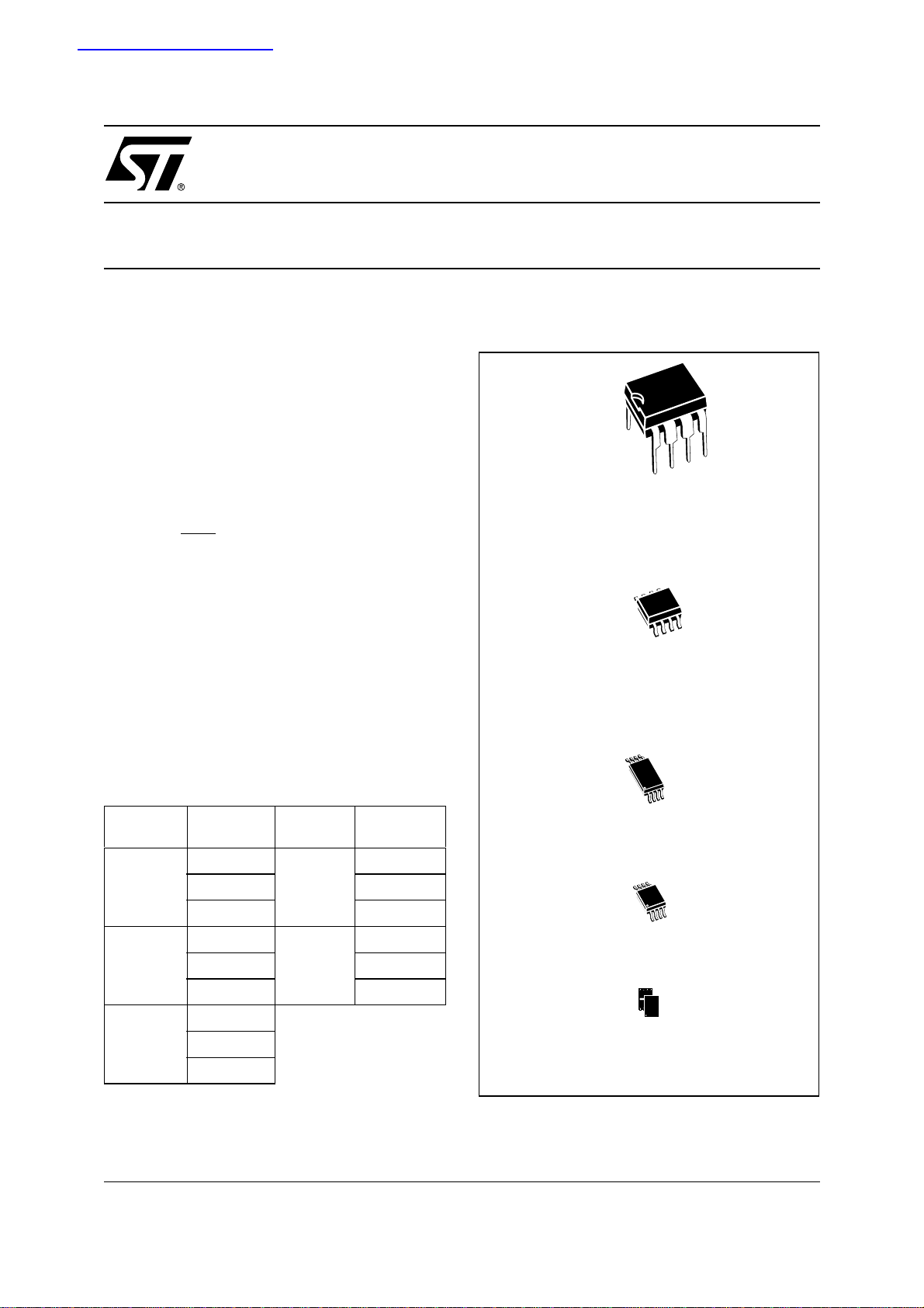
Figure 1. Packages
8
1
PDIP8 (BN)
8
1
SO8 (MN)
150 mil width
Table 1. Product List
Reference
M93C86
M93C76
M93C66
Part
Number
M93C86
M93C86-W M93C56-W
M93C86-R M93C56-R
M93C76
M93C76-W M93C46-W
M93C76-R M93C46-R
M93C66
M93C66-W
M93C66-R
Reference
M93C56
M93C46
Part
Number
M93C56
M93C46
TSSOP8 (DW)
169 mil width
TSSOP8 (DS)
3x3mm² body size (MSOP)
UFDFPN8 (MB)
2x3mm² (MLP)
1/31August 2004
Page 2

M93C86, M93C76, M93C66, M93C56, M93C46
TABLE OF CONTENTS
FEATURES SUMMARY . . . . . . . . . . . . . . . . . . . . . . . . . . . . . . . . . . . . . . . . . . . . . . . . . . . . . . . . . . . . . 1
Table 1. Product List . . . . . . . . . . . . . . . . . . . . . . . . . . . . . . . . . . . . . . . . . . . . . . . . . . . . . . . . . . . . 1
Figure 1. Packages. . . . . . . . . . . . . . . . . . . . . . . . . . . . . . . . . . . . . . . . . . . . . . . . . . . . . . . . . . . . . . 1
Figure 2. Logic Diagram . . . . . . . . . . . . . . . . . . . . . . . . . . . . . . . . . . . . . . . . . . . . . . . . . . . . . . . . . . 4
Table 2. Signal Names . . . . . . . . . . . . . . . . . . . . . . . . . . . . . . . . . . . . . . . . . . . . . . . . . . . . . . . . . . 4
Table 3. Memory Size versus Organization. . . . . . . . . . . . . . . . . . . . . . . . . . . . . . . . . . . . . . . . . . . 4
Table 4. Instruction Set for the M93Cx6 . . . . . . . . . . . . . . . . . . . . . . . . . . . . . . . . . . . . . . . . . . . . .4
Figure 3. DIP, SO, TSSOP and MLP Connections (Top View). . . . . . . . . . . . . . . . . . . . . . . . . . . . . 5
MEMORY ORGANIZATION . . . . . . . . . . . . . . . . . . . . . . . . . . . . . . . . . . . . . . . . . . . . . . . . . . . . . . . . . . 5
POWER-ON DATA PROTECTION . . . . . . . . . . . . . . . . . . . . . . . . . . . . . . . . . . . . . . . . . . . . . . . . . . . . .5
INSTRUCTIONS . . . . . . . . . . . . . . . . . . . . . . . . . . . . . . . . . . . . . . . . . . . . . . . . . . . . . . . . . . . . . . . . . . . 6
Table 5. Instruction Set for the M93C46 . . . . . . . . . . . . . . . . . . . . . . . . . . . . . . . . . . . . . . . . . . . . .6
Table 6. Instruction Set for the M93C56 and M93C66 . . . . . . . . . . . . . . . . . . . . . . . . . . . . . . . . . . 7
Table 7. Instruction Set for the M93C76 and M93C86 . . . . . . . . . . . . . . . . . . . . . . . . . . . . . . . . . . 7
Read . . . . . . . . . . . . . . . . . . . . . . . . . . . . . . . . . . . . . . . . . . . . . . . . . . . . . . . . . . . . . . . . . . . . . . . . . 8
Erase/Write Enable and Disable. . . . . . . . . . . . . . . . . . . . . . . . . . . . . . . . . . . . . . . . . . . . . . . . . . . 8
Figure 4. READ, WRITE, EWEN, EWDS Sequences. . . . . . . . . . . . . . . . . . . . . . . . . . . . . . . . . . . . 8
Erase. . . . . . . . . . . . . . . . . . . . . . . . . . . . . . . . . . . . . . . . . . . . . . . . . . . . . . . . . . . . . . . . . . . . . . . . . 9
Write . . . . . . . . . . . . . . . . . . . . . . . . . . . . . . . . . . . . . . . . . . . . . . . . . . . . . . . . . . . . . . . . . . . . . . . . . 9
Figure 5. ERASE, ERAL Sequences . . . . . . . . . . . . . . . . . . . . . . . . . . . . . . . . . . . . . . . . . . . . . . . . 9
Erase All. . . . . . . . . . . . . . . . . . . . . . . . . . . . . . . . . . . . . . . . . . . . . . . . . . . . . . . . . . . . . . . . . . . . . 10
Write All . . . . . . . . . . . . . . . . . . . . . . . . . . . . . . . . . . . . . . . . . . . . . . . . . . . . . . . . . . . . . . . . . . . . . 10
Figure 6. WRAL Sequence . . . . . . . . . . . . . . . . . . . . . . . . . . . . . . . . . . . . . . . . . . . . . . . . . . . . . . . 10
READY/BUSY STATUS . . . . . . . . . . . . . . . . . . . . . . . . . . . . . . . . . . . . . . . . . . . . . . . . . . . . . . . . . . . . 11
COMMON I/O OPERATION . . . . . . . . . . . . . . . . . . . . . . . . . . . . . . . . . . . . . . . . . . . . . . . . . . . . . . . . . 11
CLOCK PULSE COUNTER . . . . . . . . . . . . . . . . . . . . . . . . . . . . . . . . . . . . . . . . . . . . . . . . . . . . . . . . . 11
Figure 7. Write Sequence with One Clock Glitch . . . . . . . . . . . . . . . . . . . . . . . . . . . . . . . . . . . . . . 11
MAXIMUM RATING. . . . . . . . . . . . . . . . . . . . . . . . . . . . . . . . . . . . . . . . . . . . . . . . . . . . . . . . . . . . . . . . 12
Table 8. Absolute Maximum Ratings. . . . . . . . . . . . . . . . . . . . . . . . . . . . . . . . . . . . . . . . . . . . . . . 12
DC AND AC PARAMETERS. . . . . . . . . . . . . . . . . . . . . . . . . . . . . . . . . . . . . . . . . . . . . . . . . . . . . . . . . 13
Table 9. Operating Conditions (M93Cx6) . . . . . . . . . . . . . . . . . . . . . . . . . . . . . . . . . . . . . . . . . . . 13
Table 10. Operating Conditions (M93Cx6-W) . . . . . . . . . . . . . . . . . . . . . . . . . . . . . . . . . . . . . . . . . 13
Table 11. Operating Conditions (M93Cx6-R) . . . . . . . . . . . . . . . . . . . . . . . . . . . . . . . . . . . . . . . . . 13
Table 12. AC Measurement Conditions (M93Cx6) . . . . . . . . . . . . . . . . . . . . . . . . . . . . . . . . . . . . . 14
Table 13. AC Measurement Conditions (M93Cx6-W and M93Cx6-R) . . . . . . . . . . . . . . . . . . . . . . 14
Figure 8. AC Testing Input Output Waveforms. . . . . . . . . . . . . . . . . . . . . . . . . . . . . . . . . . . . . . . . 14
2/31
Page 3

M93C86, M93C76, M93C66, M93C56, M93C46
Table 14. Capacitance. . . . . . . . . . . . . . . . . . . . . . . . . . . . . . . . . . . . . . . . . . . . . . . . . . . . . . . . . . . 14
Table 15. DC Characteristics (M93Cx6, Device Grade 6). . . . . . . . . . . . . . . . . . . . . . . . . . . . . . . . 15
Table 16. DC Characteristics (M93Cx6, Device Grade 7 or 3) . . . . . . . . . . . . . . . . . . . . . . . . . . . . 15
Table 17. DC Characteristics (M93Cx6-W, Device Grade 6) . . . . . . . . . . . . . . . . . . . . . . . . . . . . . 16
Table 18. DC Characteristics (M93Cx6-W, Device Grade 7 or 3). . . . . . . . . . . . . . . . . . . . . . . . . . 17
Table 19. DC Characteristics (M93Cx6-R) . . . . . . . . . . . . . . . . . . . . . . . . . . . . . . . . . . . . . . . . . . . 17
Table 20. AC Characteristics (M93Cx6, Device Grade 6, 7 or 3) . . . . . . . . . . . . . . . . . . . . . . . . . . 18
Table 21. AC Characteristics (M93Cx6-W, Device Grade 6). . . . . . . . . . . . . . . . . . . . . . . . . . . . . . 19
Table 22. AC Characteristics (M93Cx6-W, Device Grade 7 or 3) . . . . . . . . . . . . . . . . . . . . . . . . . . 20
Table 23. AC Characteristics (M93Cx6-R) . . . . . . . . . . . . . . . . . . . . . . . . . . . . . . . . . . . . . . . . . . . 21
Figure 9. Synchronous Timing (Start and Op-Code Input) . . . . . . . . . . . . . . . . . . . . . . . . . . . . . . . 22
Figure 10.Synchronous Timing (Read or Write) . . . . . . . . . . . . . . . . . . . . . . . . . . . . . . . . . . . . . . . 22
Figure 11.Synchronous Timing (Read or Write) . . . . . . . . . . . . . . . . . . . . . . . . . . . . . . . . . . . . . . . 22
PACKAGE MECHANICAL . . . . . . . . . . . . . . . . . . . . . . . . . . . . . . . . . . . . . . . . . . . . . . . . . . . . . . . . . . 23
Figure 12.PDIP8 – 8 pin Plastic DIP, 0.25mm lead frame, Package Outline . . . . . . . . . . . . . . . . . 23
Table 24. PDIP8 – 8 pin Plastic DIP, 0.25mm lead frame, Package Mechanical Data . . . . . . . . . . 23
Figure 13.SO8 narrow – 8 lead Plastic Small Outline, 150 mils body width, Package Outline . . . . 24
Table 25. SO8 narrow – 8 lead Plastic Small Outline, 150 mils body width, Package Mechanical Data
24
Figure 14.UFDFPN8 (MLP8) 8-lead Ultra thin Fine pitch Dual Flat Package No lead 2x3mm², Outline
25
Table 26. UFDFPN8 (MLP8) 8-lead Ultra thin Fine pitch Dual Flat Package No lead 2x3mm², Data.
25
Figure 15.TSSOP8 3x3mm² – 8 lead Thin Shrink Small Outline, 3x3mm² body size, Package Outline
26
Table 27. TSSOP8 3x3mm² – 8 lead Thin Shrink Small Outline, 3x3mm² body size, Mechanical Data
26
Figure 16.TSSOP8 – 8 lead Thin Shrink Small Outline, Package Outline . . . . . . . . . . . . . . . . . . . 27
Table 28. TSSOP8 – 8 lead Thin Shrink Small Outline, Package Mechanical Data . . . . . . . . . . . . 27
PART NUMBERING . . . . . . . . . . . . . . . . . . . . . . . . . . . . . . . . . . . . . . . . . . . . . . . . . . . . . . . . . . . . . . . 28
Table 29. Ordering Information Scheme . . . . . . . . . . . . . . . . . . . . . . . . . . . . . . . . . . . . . . . . . . . . . 28
Table 30. How to Identify Current and New Products by the Process Identification Letter . . . . . . . 29
REVISION HISTORY. . . . . . . . . . . . . . . . . . . . . . . . . . . . . . . . . . . . . . . . . . . . . . . . . . . . . . . . . . . . . . . 30
Table 31. Document Revision History . . . . . . . . . . . . . . . . . . . . . . . . . . . . . . . . . . . . . . . . . . . . . . . 30
3/31
Page 4

M93C86, M93C76, M93C66, M93C56, M93C46
SUMMARY DESCRIPTION
These electrically erasable programmable memory (EEPROM) devices are accessed through a Serial Data Input (D) and Serial Data Output (Q)
using the MICROWIRE bus protocol.
Figure 2. Logic Diagram
V
CC
ORG
D
C
S
M93Cx6
V
SS
Q
AI01928
Table 3. Memory Size versus Organization
Device
M93C86 16384 2048 1024
M93C76 8192 1024 512
M93C66 4096 512 256
M93C56 2048 256 128
M93C46 1024 128 64
Number
of Bits
Number
of 8-bit
Bytes
Number
of 16-bit
Words
The M93Cx6 is accessed by a set of instructions,
as summarized in Table 4., and in more detail in
Table 5. to Table 7.).
Table 4. Instruction Set for the M93Cx6
Instruction Description Data
READ Read Data from Memory Byte or Word
WRITE Write Data to Memory Byte or Word
EWEN Erase/Write Enable
EWDS Erase/Write Disable
Table 2. Signal Names
S Chip Select Input
D Serial Data Input
Q Serial Data Output
C Serial Clock
ORG Organisation Select
V
CC
V
SS
Supply Voltage
Ground
The memory array organization may be divided
into either bytes (x8) or words (x16) which may be
selected by a signal applied on Organization Select (ORG). The bit, byte and word sizes of the
memories are as shown in Table 3..
ERASE Erase Byte or Word Byte or Word
ERAL Erase All Memory
WRAL
Write All Memory
with same Data
A Read Data from Memory (READ) instruction
loads the address of the first byte or word to be
read in an internal address register. The data at
this address is then clocked out serially. The address register is automatically incremented after
the data is output and, if Chip Select Input (S) is
held High, the M93Cx6 can output a sequential
stream of data bytes or words. In this way, the
memory can be read as a data stream from eight
to 16384 bits long (in the case of the M93C86), or
continuously (the address counter automatically
rolls over to 00h when the highest address is
reached).
Programming is internally self-timed (the external
clock signal on Serial Clock (C) may be stopped or
left running after the start of a Write cycle) and
does not require an Erase cycle prior to the Write
instruction. The Write instruction writes 8 or 16 bits
at a time into one of the byte or word locations of
the M93Cx6. After the start of the programming cycle, a Busy/Ready signal is available on Serial
Data Output (Q) when Chip Select Input (S) is driven High.
4/31
Page 5
M93C86, M93C76, M93C66, M93C56, M93C46
An internal Power-on Data Protection mechanism
in the M93Cx6 inhibits the device when the supply
is too low.
Figure 3. DIP, SO, TSSOP and MLP
Connections (Top View)
M93Cx6
SV
1
2
D
3
Q
4
Note: 1. See PACKAGE MECHANICAL section for package di-
mensions, and how to identify pin-1.
2. DU = Don’t Use.
8
7
6
5
AI01929B
CC
DUC
ORG
V
SS
The DU (Don’t Use) pin does not contribute to the
normal operation of the device. It is reserved for
use by STMicroelectronics during test sequences.
The pin may be left unconnected or may be connected to V
is recommended for the lowest stand-by pow-
V
SS
or VSS. Direct connection of DU to
CC
er consumption.
MEMORY ORGANIZATION
The M93Cx6 memory is organized either as bytes
(x8) or as words (x16). If Organization Select
(ORG) is left unconnected (or connected to V
CC
the x16 organization is selected; when Organization Select (ORG) is connected to Ground (V
SS
the x8 organization is selected. When the M93Cx6
is in stand-by mode, Organization Select (ORG)
should be set either to V
power consumption. Any voltage between V
or VCC for minimum
SS
SS
and VCC applied to Organization Select (ORG)
may increase the stand-by current.
POWER-ON DATA PROTECTION
To prevent data corruption and inadvertent write
operations during power-up, a Power-On Reset
(POR) circuit resets all internal programming circuitry, and sets the device in the Write Disable
mode.
– At Power-up and Power-down, the device
must not be selected (that is, Chip Select Input
(S) must be driven Low) until the supply
voltage reaches the operating value V
specified in Table 9. to Table 11..
– When V
reaches its valid level, the device is
CC
properly reset (in the Write Disable mode) and
is ready to decode and execute incoming
instructions.
For the M93Cx6 devices (5V range) the POR
threshold voltage is around 3V. For the M93Cx6W (3V range) and M93Cx6-R (2V range) the POR
threshold voltage is around 1.5V.
CC
)
)
5/31
Page 6

M93C86, M93C76, M93C66, M93C56, M93C46
INSTRUCTIONS
The instruction set of the M93Cx6 devices contains seven instructions, as summarized in Table
5. to Table 7.. Each instruction consists of the fol-
lowing parts, as shown in Figure 4.:
■ Each instruction is preceded by a rising edge
on Chip Select Input (S) with Serial Clock (C)
being held Low.
■ A start bit, which is the first ‘1’ read on Serial
Data Input (D) during the rising edge of Serial
Clock (C).
■ Two op-code bits, read on Serial Data Input
(D) during the rising edge of Serial Clock (C).
(Some instructions also use the first two bits of
the address to define the op-code).
Table 5. Instruction Set for the M93C46
x8 Origination (ORG = 0) x16 Origination (ORG = 1)
Instruc
tion
Description
Start
bit
Op-
Code
Address
1
■ The address bits of the byte or word that is to
be accessed. For the M93C46, the address is
made up of 6 bits for the x16 organization or 7
bits for the x8 organization (see Table 5.). For
the M93C56 and M93C66, the address is
made up of 8 bits for the x16 organization or 9
bits for the x8 organization (see Table 6.). For
the M93C76 and M93C86, the address is
made up of 10 bits for the x16 organization or
11 bits for the x8 organization (see Table 7.).
The M93Cx6 devices are fabricated in CMOS
technology and are therefore able to run as slow
as 0 Hz (static input signals) or as fast as the maximum ratings specified in Table 20. to Table 23..
Data
Required
Clock
Cycles
Address
1
Data
Required
Clock
Cycles
READ
WRITE
EWEN Erase/Write Enable 1 00 11X XXXX 10 11 XXXX 9
EWDS Erase/Write Disable 1 00 00X XXXX 10 00 XXXX 9
ERASE Erase Byte or Word 1 11 A6-A0 10 A5-A0 9
ERAL Erase All Memory 1 00 10X XXXX 10 10 XXXX 9
WRAL
Note: 1. X = Don’t Care bit.
Read Data from
Memory
Write Data to
Memory
Write All Memory
with same Data
1 10 A6-A0 Q7-Q0 A5-A0 Q15-Q0
1 01 A6-A0 D7-D0 18 A5-A0 D15-D0 25
1 00 01X XXXX D7-D0 18 01 XXXX D15-D0 25
6/31
Page 7
M93C86, M93C76, M93C66, M93C56, M93C46
Table 6. Instruction Set for the M93C56 and M93C66
x8 Origination (ORG = 0) x16 Origination (ORG = 1)
Instruc
tion
READ
WRITE
Description
Read Data from
Memory
Write Data to
Memory
EWEN Erase/Write Enable 1 00
EWDS Erase/Write Disable 1 00
ERASE Erase Byte or Word 1 11 A8-A0 12 A7-A0 11
ERAL Erase All Memory 1 00
WRAL
Note: 1. X = Don’t Care bit.
Write All Memory
with same Data
2. Address bit A8 is not decoded by the M93C56.
3. Address bit A7 is not decoded by the M93C56.
Start
bit
Op-
Code
Address
1,2
Data
Required
Clock
Address
1,3
Required
Data
Cycles
1 10 A8-A0 Q7-Q0 A7-A0 Q15-Q0
1 01 A8-A0 D7-D0 20 A7-A0 D15-D0 27
100
1 1XXX
XXXX
0 0XXX
XXXX
1 0XXX
XXXX
0 1XXX
XXXX
12
12
12
D7-D0 20
11XX
XXXX
00XX
XXXX
10XX
XXXX
01XX
XXXX
D15-D0 27
Clock
Cycles
11
11
11
Table 7. Instruction Set for the M93C76 and M93C86
x8 Origination (ORG = 0) x16 Origination (ORG = 1)
Instruc
tion
READ
WRITE
Description
Read Data from
Memory
Write Data to
Memory
EWEN Erase/Write Enable 1 00
EWDS Erase/Write Disable 1 00
ERASE Erase Byte or Word 1 11 A10-A0 14 A9-A0 13
ERAL Erase All Memory 1 00
WRAL
Note: 1. X = Don’t Care bit.
Write All Memory
with same Data
2. Address bit A10 is not decoded by the M93C76.
3. Address bit A9 is not decoded by the M93C76.
Start
bit
Op-
Code
Address
1,2
Data
Required
Clock
Address
1,3
Required
Data
Cycles
1 10 A10-A0 Q7-Q0 A9-A0 Q15-Q0
1 01 A10-A0 D7-D0 22 A9-A0 D15-D0 29
100
11X XXXX
XXXX
00X XXXX
XXXX
10X XXXX
XXXX
01X XXXX
XXXX
14
14
14
D7-D0 22
11 XXXX
XXXX
00 XXXX
XXXX
10 XXXX
XXXX
01 XXXX
XXXX
D15-D0 29
Clock
Cycles
13
13
13
7/31
Page 8

M93C86, M93C76, M93C66, M93C56, M93C46
Read
The Read Data from Memory (READ) instruction
outputs data on Serial Data Output (Q). When the
instruction is received, the op-code and address
are decoded, and the data from the memory is
transferred to an output shift register. A dummy 0
bit is output first, followed by the 8-bit byte or 16bit word, with the most significant bit first. Output
data changes are triggered by the rising edge of
Serial Clock (C). The M93Cx6 automatically increments the internal address register and clocks out
the next byte (or word) as long as the Chip Select
Input (S) is held High. In this case, the dummy 0 bit
is not output between bytes (or words) and a continuous stream of data can be read.
Figure 4. READ, WRITE, EWEN, EWDS Sequences
READ
S
D
1 1 0 An A0
Erase/Write Enable and Disable
The Erase/Write Enable (EWEN) instruction enables the future execution of erase or write instructions, and the Erase/Write Disable (EWDS)
instruction disables it. When power is first applied,
the M93Cx6 initializes itself so that erase and write
instructions are disabled. After an Erase/Write Enable (EWEN) instruction has been executed, erasing and writing remains enabled until an Erase/
Write Disable (EWDS) instruction is executed, or
until V
falls below the power-on reset threshold
CC
voltage. To protect the memory contents from accidental corruption, it is advisable to issue the
Erase/Write Disable (EWDS) instruction after every write cycle. The Read Data from Memory
(READ) instruction is not affected by the Erase/
Write Enable (EWEN) or Erase/Write Disable
(EWDS) instructions.
Q
ADDR
OP
CODE
SWRITE
D
Q
SERASE
WRITE
ENABLE
D
Note: For the meanings of An, Xn, Qn and Dn, see Table 5., Table 6. and Table 7..
1 0An A0
ADDR
OP
CODE
1
0XnX0
101
OP
CODE
Qn Q0
DATA OUT
Dn D01
DATA IN
WRITE
DISABLE
CHECK
STATUS
BUSY READY
SERASE
D
1
0XnX0
0 00
OP
CODE
AI00878C
8/31
Page 9
M93C86, M93C76, M93C66, M93C56, M93C46
Erase
The Erase Byte or Word (ERASE) instruction sets
the bits of the addressed memory byte (or word) to
1. Once the address has been correctly decoded,
the falling edge of the Chip Select Input (S) starts
the self-timed Erase cycle. The completion of the
cycle can be detected by monitoring the Ready/
line, as described in the READY/BUSY STA-
Busy
TUS section.
Write
For the Write Data to Memory (WRITE) instruction,
8 or 16 data bits follow the op-code and address
bits. These form the byte or word that is to be written. As with the other bits, Serial Data Input (D) is
sampled on the rising edge of Serial Clock (C).
Figure 5. ERASE, ERAL Sequences
SERASE
1 1D
1
An A0
Q
After the last data bit has been sampled, the Chip
Select Input (S) must be taken Low before the next
rising edge of Serial Clock (C). If Chip Select Input
(S) is brought Low before or after this specific time
frame, the self-timed programming cycle will not
be started, and the addressed location will not be
programmed. The completion of the cycle can be
detected by monitoring the Ready/Busy
line, as
described later in this document.
Once the Write cycle has been started, it is inter-
nally self-timed (the external clock signal on Serial
Clock (C) may be stopped or left running after the
start of a Write cycle). The cycle is automatically
preceded by an Erase cycle, so it is unnecessary
to execute an explicit erase instruction before a
Write Data to Memory (WRITE) instruction.
CHECK
STATUS
ADDR
OP
CODE
ALL
Note: For the meanings of An and Xn, please see Table 5., Table 6. and Table 7..
SERASE
1 0D
1
0 0
Xn X0
Q
ADDR
OP
CODE
BUSY READY
CHECK
STATUS
BUSY READY
AI00879B
9/31
Page 10

M93C86, M93C76, M93C66, M93C56, M93C46
Erase All
The Erase All Memory (ERAL) instruction erases
the whole memory (all memory bits are set to 1).
The format of the instruction requires that a dummy address be provided. The Erase cycle is conducted in the same way as the Erase instruction
(ERASE). The completion of the cycle can be detected by monitoring the Ready/Busy
line, as de-
scribed in the READY/BUSY STATUS section.
Write All
As with the Erase All Memory (ERAL) instruction,
the format of the Write All Memory with same Data
(WRAL) instruction requires that a dummy address be provided. As with the Write Data to Memory (WRITE) instruction, the format of the Write All
Memory with same Data (WRAL) instruction requires that an 8-bit data byte, or 16-bit data word,
be provided. This value is written to all the addresses of the memory device. The completion of
the cycle can be detected by monitoring the
Ready/Busy
Figure 6. WRAL Sequence
ALL
Note: For the meanings of Xn and Dn, please see Table 5., Table 6. and Table 7..
SWRITE
D
Q
1
OP
CODE
0
Xn X0
00 1
Dn D0
ADDR
DATA IN
line, as described next.
CHECK
STATUS
BUSY READY
AI00880C
10/31
Page 11

READY/BUSY STATUS
While the Write or Erase cycle is underway, for a
WRITE, ERASE, WRAL or ERAL instruction, the
Busy signal (Q=0) is returned whenever Chip Select Input (S) is driven High. (Please note, though,
that there is an initial delay, of t
, before this
SLSH
status information becomes available). In this
state, the M93Cx6 ignores any data on the bus.
When the Write cycle is completed, and Chip Select Input (S) is driven High, the Ready signal
(Q=1) indicates that the M93Cx6 is ready to receive the next instruction. Serial Data Output (Q)
remains set to 1 until the Chip Select Input (S) is
brought Low or until a new start bit is decoded.
COMMON I/O OPERATION
Serial Data Output (Q) and Serial Data Input (D)
can be connected together, through a current limiting resistor, to form a common, single-wire data
bus. Some precautions must be taken when operating the memory in this way, mostly to prevent a
short circuit current from flowing when the last address bit (A0) clashes with the first data bit on Serial Data Output (Q). Please see the application
note AN394 for details.
M93C86, M93C76, M93C66, M93C56, M93C46
CLOCK PULSE COUNTER
In a noisy environment, the number of pulses received on Serial Clock (C) may be greater than the
number delivered by the master (the microcontroller). This can lead to a misalignment of the instruction of one or more bits (as shown in Figure 7.) and
may lead to the writing of erroneous data at an erroneous address.
To combat this problem, the M93Cx6 has an onchip counter that counts the clock pulses from the
start bit until the falling edge of the Chip Select Input (S). If the number of clock pulses received is
not the number expected, the WRITE, ERASE,
ERAL or WRAL instruction is aborted, and the
contents of the memory are not modified.
The number of clock cycles expected for each instruction, and for each member of the M93Cx6
family, are summarized in Table 5. to Table 7.. For
example, a Write Data to Memory (WRITE) instruction on the M93C56 (or M93C66) expects 20
clock cycles (for the x8 organization) from the start
bit to the falling edge of Chip Select Input (S). That
is:
1 Start bit
+ 2 Op-code bits
+ 9 Address bits
+ 8 Data bits
Figure 7. Write Sequence with One Clock Glitch
S
C
D
An
START
WRITE
An-1
Glitch
An-2
ADDRESS AND DATA
ARE SHIFTED BY ONE BIT
D0"1""0"
AI01395
11/31
Page 12

M93C86, M93C76, M93C66, M93C56, M93C46
MAXIMUM RATING
Stressing the device above the rating listed in the
Absolute Maximum Ratings" table may cause permanent damage to the device. These are stress
ratings only and operation of the device at these or
any other conditions above those indicated in the
Operating sections of this specification is not im-
Table 8. Absolute Maximum Ratings
Symbol Parameter Min. Max. Unit
T
T
LEAD
Storage Temperature –65 150 °C
STG
Lead Temperature during Soldering
plied. Exposure to Absolute Maximum Rating conditions for extended periods may affect device
reliability. Refer also to the STMicroelectronics
SURE Program and other relevant quality documents.
See note
1
°C
V
V
V
V
Note: 1. Compliant with JEDEC Std J-STD-020B (for small body, Sn-Pb or Pb assembly), the ST ECOPACK® 7191395 specification, and
Output range (Q = VOH or Hi-Z)
OUT
Input range –0.50 VCC+1 V
IN
Supply Voltage –0.50 6.5 V
CC
ESD Electrostatic Discharge Voltage (Human Body model)
the European directive on Restrictions on Hazardous Substances (RoHS) 2002/95/EU
2. JEDEC Std JESD22-A114A (C1=100 pF, R1=1500
Ω, R2=500 Ω)
2
–0.50 V
CC
–4000 4000 V
+0.5 V
12/31
Page 13

M93C86, M93C76, M93C66, M93C56, M93C46
DC AND AC PARAMETERS
This section summarizes the operating and measurement conditions, and the DC and AC characteristics of the device. The parameters in the DC
and AC Characteristic tables that follow are derived from tests performed under the Measure-
Table 9. Operating Conditions (M93Cx6)
Symbol Parameter Min. Max. Unit
ment Conditions summarized in the relevant
tables. Designers should check that the operating
conditions in their circuit match the measurement
conditions when relying on the quoted parameters.
V
CC
T
A
Supply Voltage 4.5 5.5 V
Ambient Operating Temperature (Device Grade 6) –40 85 °C
Ambient Operating Temperature (Device Grade 7) –40 105 °C
Ambient Operating Temperature (Device Grade 3) –40 125 °C
Table 10. Operating Conditions (M93Cx6-W)
Symbol Parameter Min. Max. Unit
V
CC
T
A
Supply Voltage 2.5 5.5 V
Ambient Operating Temperature (Device Grade 6) –40 85 °C
Ambient Operating Temperature (Device Grade 7) –40 105 °C
Ambient Operating Temperature (Device Grade 3) –40 125 °C
Table 11. Operating Conditions (M93Cx6-R)
Symbol Parameter Min. Max. Unit
V
CC
T
A
Supply Voltage 1.8 5.5 V
Ambient Operating Temperature (Device Grade 6) –40 85 °C
13/31
Page 14

M93C86, M93C76, M93C66, M93C56, M93C46
Table 12. AC Measurement Conditions (M93Cx6)
Symbol Parameter Min. Max. Unit
C
L
Load Capacitance 100 pF
Input Rise and Fall Times 50 ns
Input Pulse Voltages 0.4 V to 2.4 V V
Input Timing Reference Voltages 1.0 V and 2.0 V V
Output Timing Reference Voltages 0.8 V and 2.0 V V
Note: 1. Output Hi-Z is defined as the point where data out is no longer driven.
Table 13. AC Measurement Conditions (M93Cx6-W and M93Cx6-R)
Symbol Parameter Min. Max. Unit
C
L
Load Capacitance 100 pF
Input Rise and Fall Times 50 ns
to 0.8V
Input Pulse Voltages
Input Timing Reference Voltages
Output Timing Reference Voltages
Note: 1. Output Hi-Z is defined as the point where data out is no longer driven.
0.2V
0.3V
0.3V
CC
to 0.7V
CC
to 0.7V
CC
CC
CC
CC
Figure 8. AC Testing Input Output Waveforms
V
V
V
M93CXX
2V
1V
M93CXX-W & M93CXX-R
2.0V
0.8V
0.7V
0.3V
AI02553
CC
CC
0.8V
0.2V
2.4V
0.4V
INPUT OUTPUT
CC
CC
Table 14. Capacitance
Symbol Parameter Test Condition Min Max Unit
C
OUT
C
IN
Note: Sampled only, not 100% tested, at TA=25°C and a frequency of 1MHz.
Output
Capacitance
Input
Capacitance
V
OUT
V
IN
= 0V
= 0V
5pF
5pF
14/31
Page 15

M93C86, M93C76, M93C66, M93C56, M93C46
Table 15. DC Characteristics (M93Cx6, Device Grade 6)
Symbol Parameter Test Condition Min. Max. Unit
0V
≤ V
I
I
I
I
CC1
V
V
V
V
Note: 1. Current product: identified by Process Identification letter F or M.
Input Leakage Current
LI
0V
Output Leakage Current
LO
V
Supply Current
CC
ORG = V
Supply Current (Stand-by)
Input Low Voltage
IL
Input High Voltage
IH
Output Low Voltage
OL
Output High Voltage
OH
2. New product: identified by Process Identification letter W or G or S.
≤ V
OUT
= 5V, S = VIH, f = 1 MHz, Current
CC
V
= 5V, S = VIH, f = 2 MHz, New
CC
= 5V, S = VSS, C = VSS,
V
CC
or VCC, Current Product
SS
V
= 5V, S = VSS, C = VSS,
CC
ORG = V
SS
V
V
V
= 5V, IOL = 2.1mA
CC
V
= 5V, IOH = –400µA
CC
≤ V
IN
CC
≤ VCC, Q in Hi-Z
Product
Product
1
2
or VCC, New Product
= 5V ± 10%
CC
= 5V ± 10%
CC
±2.5 µA
±2.5 µA
1.5 mA
2 mA
1
2
50 µA
15 µA
–0.45 0.8 V
2
VCC + 1
0.4 V
2.4 V
V
Table 16. DC Characteristics (M93Cx6, Device Grade 7 or 3)
Symbol Parameter Test Condition Min. Max. Unit
0V
≤ V
I
I
I
I
CC1
V
V
V
V
Note: 1. Current product: identified by Process Identification letter F or M.
Input Leakage Current
LI
0V
Output Leakage Current
LO
V
Supply Current
CC
ORG = V
Supply Current (Stand-by)
Input Low Voltage
IL
Input High Voltage
IH
Output Low Voltage
OL
Output High Voltage
OH
2. New product: identified by Process Identification letter W or G or S.
≤ V
OUT
= 5V, S = VIH, f = 1 MHz, Current
CC
V
= 5V, S = VIH, f = 2 MHz, New
CC
= 5V, S = VSS, C = VSS,
V
CC
or VCC, Current Product
SS
V
= 5V, S = VSS, C = VSS,
CC
ORG = V
SS
V
V
V
= 5V, IOL = 2.1mA
CC
V
= 5V, IOH = –400µA
CC
≤ V
IN
CC
≤ VCC, Q in Hi-Z
Product
Product
1
2
or VCC, New Product
= 5V ± 10%
CC
= 5V ± 10%
CC
±2.5 µA
±2.5 µA
1.5 mA
2 mA
1
2
50 µA
15 µA
–0.45 0.8 V
2
VCC + 1
0.4 V
2.4 V
V
15/31
Page 16

M93C86, M93C76, M93C66, M93C56, M93C46
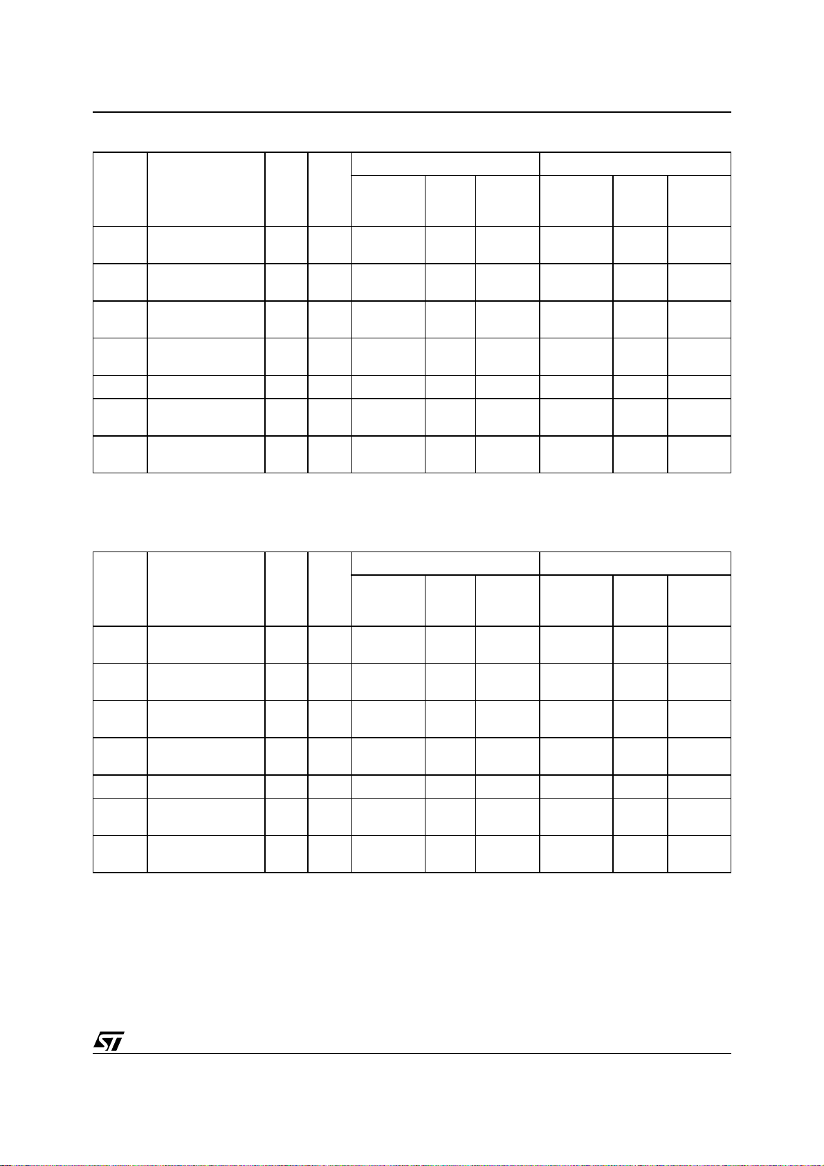
Table 17. DC Characteristics (M93Cx6-W, Device Grade 6)
Symbol Parameter Test Condition Min. Max. Unit
0V
≤ V
I
I
I
I
CC1
V
V
V
V
Note: 1. Current product: identified by Process Identification letter F or M.
Input Leakage Current
LI
0V
Output Leakage Current
LO
V
V
CC
Supply Current (CMOS
CC
Inputs)
V
ORG = V
Supply Current (Stand-by)
Input Low Voltage (D, C, S) –0.45
IL
Input High Voltage (D, C, S)
IH
Output Low Voltage (Q)
OL
Output High Voltage (Q)
OH
2. New product: identified by Process Identification letter W or G or S.
≤ V
OUT
= 5V, S = VIH, f = 1 MHz, Current
CC
= 2.5V, S = VIH, f = 1 MHz, Current
V
= 5V, S = VIH, f = 2 MHz, New
CC
= 2.5V, S = VIH, f = 2 MHz, New
CC
= 2.5V, S = VSS, C = VSS,
V
CC
or VCC, Current Product
SS
V
= 2.5V, S = VSS, C = VSS,
CC
ORG = V
SS
V
= 5V, IOL = 2.1mA
CC
V
= 2.5V, IOL = 100µA
CC
V
= 5V, IOH = –400µA
CC
V
= 2.5V, IOH = –100µA VCC–0.2
CC
≤ V
IN
CC
≤ VCC, Q in Hi-Z
Product
Product
Product
Product
1
1
2
2
or VCC, New Product
±2.5 µA
±2.5 µA
1.5 mA
1 mA
2 mA
1 mA
1
2
10 µA
5 µA
0.2 V
CC
0.7 V
CC
VCC + 1
0.4 V
0.2 V
2.4 V
V
V
V
16/31
Page 17

M93C86, M93C76, M93C66, M93C56, M93C46
Table 18. DC Characteristics (M93Cx6-W, Device Grade 7 or 3)
Symbol Parameter Test Condition
0V
≤ V
I
I
I
I
CC1
V
V
V
V
Note: 1. New product: identified by Process Identification letter W or G or S.
LO
CC
Input Leakage Current
LI
0V
Output Leakage Current
Supply Current (CMOS
Inputs)
Supply Current (Stand-by)
Input Low Voltage (D, C, S) –0.45
IL
Input High Voltage (D, C, S)
IH
Output Low Voltage (Q)
OL
Output High Voltage (Q)
OH
≤ V
OUT
V
= 5V, S = VIH, f = 2 MHz
CC
V
= 2.5V, S = VIH, f = 2 MHz
CC
= 2.5V, S = VSS, C = VSS,
V
CC
ORG = V
V
= 5V, IOL = 2.1mA
CC
= 2.5V, IOL = 100µA
V
CC
V
= 5V, IOH = –400µA
CC
V
= 2.5V, IOH = –100µA VCC–0.2
CC
≤ V
IN
CC
≤ VCC, Q in Hi-Z
or V
SS
CC
Min.
1
Max.
1
Unit
±2.5 µA
±2.5 µA
2 mA
1 mA
5 µA
0.7 V
CC
0.2 V
VCC + 1
CC
V
V
0.4 V
0.2 V
2.4 V
V
Table 19. DC Characteristics (M93Cx6-R)
Symbol Parameter Test Condition
0V
≤ V
I
I
I
I
CC1
V
V
V
V
Note: 1. This product is under development. For more infomation, please contact your nearest ST sales office.
LO
CC
Input Leakage Current
LI
0V
Output Leakage Current
Supply Current (CMOS
Inputs)
Supply Current (Stand-by)
Input Low Voltage (D, C, S) –0.45
IL
Input High Voltage (D, C, S)
IH
Output Low Voltage (Q)
OL
Output High Voltage (Q)
OH
≤ V
OUT
V
= 5V, S = VIH, f = 2 MHz
CC
= 1.8V, S = VIH, f = 1 MHz
V
CC
= 1.8V, S = VSS, C = VSS,
V
CC
ORG = V
V
= 1.8V, IOL = 100µA
CC
V
= 1.8V, IOH = –100µA VCC–0.2
CC
≤ V
IN
CC
≤ VCC, Q in Hi-Z
or V
SS
CC
Min.
0.8 V
1
Max.
1
Unit
±2.5 µA
±2.5 µA
2 mA
1 mA
2 µA
CC
0.2 V
VCC + 1
CC
V
V
0.2 V
V
17/31
Page 18

M93C86, M93C76, M93C66, M93C56, M93C46
Table 20. AC Characteristics (M93Cx6, Device Grade 6, 7 or 3)
Test conditions specified in Table 12. and Table 9.
Symbol Alt. Parameter
f
t
SLCH
C
f
Clock Frequency D.C. 1 D.C. 2 MHz
SK
Chip Select Low to Clock High 250 50 ns
Chip Select Set-up Time
t
SHCH
t
CSS
M93C46, M93C56, M93C66
Chip Select Set-up time
M93C76, M93C86
2
1
1
CHCL
+ t
t
t
SKH
t
SKL
t
t
t
SKS
t
CSH
t
t
t
PD0
t
PD1
t
t
SLSH
t
CHCL
t
CLCH
t
DVC H
t
CHDX
t
CLSH
t
CLSL
t
SHQV
t
SLQZ
t
CHQL
t
CHQV
t
W
Note: 1. t
2. Chip Select Input (S) must be brought Low for a minimum of tSLSH between consecutive instruction cycles.
3. Current product: identified by Process Identification letter F or M.
4. New product: identified by Process Identification letter W or G or S.
Chip Select Low to Chip Select High 250 200 ns
CS
Clock High Time 250 200 ns
Clock Low Time 250 200 ns
Data In Set-up Time 100 50 ns
DIS
Data In Hold Time 100 50 ns
DIH
Clock Set-up Time (relative to S) 100 50 ns
Chip Select Hold Time 0 0 ns
Chip Select to Ready/Busy Status 400 200 ns
SV
Chip Select Low to Output Hi-Z 200 100 ns
DF
Delay to Output Low 400 200 ns
Delay to Output Valid 400 200 ns
Erase/Write Cycle time 10 5 ms
WP
≥ 1 / fC.
CLCH
3
Min.
50 50 ns
100 50 ns
Max.
3
Min.
4
Max.
4
Unit
18/31
Page 19

M93C86, M93C76, M93C66, M93C56, M93C46
Table 21. AC Characteristics (M93Cx6-W, Device Grade 6)
Test conditions specified in Table 13. and Table 10.
Symbol Alt. Parameter
2
1
1
CHCL
f
Clock Frequency D.C. 1 D.C. 2 MHz
SK
Chip Select Low to Clock High 250 50 ns
+ t
t
CSS
t
t
SKH
t
SKL
t
t
t
SKS
t
CSH
t
t
t
PD0
t
PD1
t
Chip Select Set-up Time 100 50 ns
Chip Select Low to Chip Select High 1000 200 ns
CS
Clock High Time 350 200 ns
Clock Low Time 250 200 ns
Data In Set-up Time 100 50 ns
DIS
Data In Hold Time 100 50 ns
DIH
Clock Set-up Time (relative to S) 100 50 ns
Chip Select Hold Time 0 0 ns
Chip Select to Ready/Busy Status 400 200 ns
SV
Chip Select Low to Output Hi-Z 200 100 ns
DF
Delay to Output Low 400 200 ns
Delay to Output Valid 400 200 ns
Erase/Write Cycle time 10 5 ms
WP
≥ 1 / fC.
CLCH
f
C
t
SLCH
t
SHCH
t
SLSH
t
CHCL
t
CLCH
t
DVC H
t
CHDX
t
CLSH
t
CLSL
t
SHQV
t
SLQZ
t
CHQL
t
CHQV
t
W
Note: 1. t
2. Chip Select Input (S) must be brought Low for a minimum of tSLSH between consecutive instruction cycles.
3. Current product: identified by Process Identification letter F or M.
4. New product: identified by Process Identification letter W or G or S.
Min.
3
Max.
3
Min.
4
Max.
4
Unit
19/31
Page 20

M93C86, M93C76, M93C66, M93C56, M93C46
Table 22. AC Characteristics (M93Cx6-W, Device Grade 7 or 3)
Test conditions specified in Table 13. and Table 10.
Symbol Alt. Parameter
f
C
t
SLCH
t
SHCH
2
t
SLSH
1
t
CHCL
1
t
CLCH
t
DVC H
t
CHDX
t
CLSH
t
CLSL
t
SHQV
t
SLQZ
t
CHQL
t
CHQV
t
W
Note: 1. t
CHCL
2. Chip Select Input (S) must be brought Low for a minimum of tSLSH between consecutive instruction cycles.
3. New product: identified by Process Identification letter W or G or S.
f
SK
Clock Frequency D.C. 2 MHz
Chip Select Low to Clock High 50 ns
+ t
CLCH
t
CSS
t
CS
t
SKH
t
SKL
t
DIS
t
DIH
t
SKS
t
CSH
t
SV
t
DF
t
PD0
t
PD1
t
WP
≥ 1 / fC.
Chip Select Set-up Time 50 ns
Chip Select Low to Chip Select High 200 ns
Clock High Time 200 ns
Clock Low Time 200 ns
Data In Set-up Time 50 ns
Data In Hold Time 50 ns
Clock Set-up Time (relative to S) 50 ns
Chip Select Hold Time 0 ns
Chip Select to Ready/Busy Status 200 ns
Chip Select Low to Output Hi-Z 100 ns
Delay to Output Low 200 ns
Delay to Output Valid 200 ns
Erase/Write Cycle time 5 ms
Min.
3
Max.
3
Unit
20/31
Page 21

M93C86, M93C76, M93C66, M93C56, M93C46
Table 23. AC Characteristics (M93Cx6-R)
Test conditions specified in Table 13. and Table 11.
Symbol Alt. Parameter
f
C
t
SLCH
t
SHCH
2
t
SLSH
1
t
CHCL
1
t
CLCH
t
DVC H
t
CHDX
t
CLSH
t
CLSL
t
SHQV
t
SLQZ
t
CHQL
t
CHQV
t
W
Note: 1. t
CHCL
2. Chip Select Input (S) must be brought Low for a minimum of tSLSH between consecutive instruction cycles.
3. This product is under development. For more infomation, please contact your nearest ST sales office.
f
SK
Clock Frequency D.C. 1 MHz
Chip Select Low to Clock High 250 ns
+ t
CLCH
t
CSS
t
CS
t
SKH
t
SKL
t
DIS
t
DIH
t
SKS
t
CSH
t
SV
t
DF
t
PD0
t
PD1
t
WP
≥ 1 / fC.
Chip Select Set-up Time 50 ns
Chip Select Low to Chip Select High 250 ns
Clock High Time 250 ns
Clock Low Time 250 ns
Data In Set-up Time 100 ns
Data In Hold Time 100 ns
Clock Set-up Time (relative to S) 100 ns
Chip Select Hold Time 0 ns
Chip Select to Ready/Busy Status 400 ns
Chip Select Low to Output Hi-Z 200 ns
Delay to Output Low 400 ns
Delay to Output Valid 400 ns
Erase/Write Cycle time 10 ms
Min.
3
Max.
3
Unit
21/31
Page 22

M93C86, M93C76, M93C66, M93C56, M93C46
Figure 9. Synchronous Timing (Start and Op-Code Input)
tCLSH tCHCL
C
tSHCH
S
tDVCH
D
START
Figure 10. Synchronous Timing (Read or Write)
C
S
tDVCH
A0
Hi-Z
An
tCHQL
D
Q
tCLCH
OP CODE OP CODE
OP CODE INPUTSTART
tCHQVtCHDX
Q15/Q7 Q0
tCHDX
AI01428
tCLSL
tSLSH
tSLQZ
ADDRESS INPUT
Figure 11. Synchronous Timing (Read or Write)
C
S
tDVCH
D
Q
An
Hi-Z
ADDRESS/DATA INPUT
A0/D0
tSLCH
tCLSL
tSLSHtCHDX
DATA OUTPUT
tSHQV
tW
WRITE CYCLE
tSLQZ
BUSY
AI00820C
READY
AI01429
22/31
Page 23

M93C86, M93C76, M93C66, M93C56, M93C46
PACKAGE MECHANICAL
Figure 12. PDIP8 – 8 pin Plastic DIP, 0.25mm lead frame, Package Outline
b2
A2
A1AL
be
D
8
E1
1
Note: Drawing is not to scale.
E
c
eA
eB
PDIP-B
Table 24. PDIP8 – 8 pin Plastic DIP, 0.25mm lead frame, Package Mechanical Data
Symb.
Typ. Min. Max. Typ. Min. Max.
A 5.33 0.210
mm inches
A1 0.38 0.015
A2 3.30 2.92 4.95 0.130 0.115 0.195
b 0.46 0.36 0.56 0.018 0.014 0.022
b2 1.52 1.14 1.78 0.060 0.045 0.070
c 0.25 0.20 0.36 0.010 0.008 0.014
D 9.27 9.02 10.16 0.365 0.355 0.400
E 7.87 7.62 8.26 0.310 0.300 0.325
E1 6.35 6.10 7.11 0.250 0.240 0.280
e2.54––0.100 ––
eA 7.62 ––0.300 ––
eB 10.92 0.430
L 3.30 2.92 3.81 0.130 0.115 0.150
23/31
Page 24

M93C86, M93C76, M93C66, M93C56, M93C46
Figure 13. SO8 narrow – 8 lead Plastic Small Outline, 150 mils body width, Package Outline
h x 45˚
Note: Drawing is not to scale.
B
SO-a
A
e
D
N
1
CP
E
H
C
LA1 α
Table 25. SO8 narrow – 8 lead Plastic Small Outline, 150 mils body width, Package Mechanical Data
Symb.
Typ. Min. Max. Typ. Min. Max.
A 1.35 1.75 0.053 0.069
A1 0.10 0.25 0.004 0.010
B 0.33 0.51 0.013 0.020
mm inches
24/31
C 0.19 0.25 0.007 0.010
D 4.80 5.00 0.189 0.197
E 3.80 4.00 0.150 0.157
e1.27––0.050 ––
H 5.80 6.20 0.228 0.244
h 0.25 0.50 0.010 0.020
L 0.40 0.90 0.016 0.035
α 0° 8° 0° 8°
N8 8
CP 0.10 0.004
Page 25

M93C86, M93C76, M93C66, M93C56, M93C46
Figure 14. UFDFPN8 (MLP8) 8-lead Ultra thin Fine pitch Dual Flat Package No lead 2x3mm², Outline
e
D
b
L3
E
A
ddd
A1
Note: 1. Drawing is not to scale.
2. The central pad (the area E2 by D2 in the above illustration) is pulled, internally, to V
any other voltage or signal line on the PCB, for example during the soldering process.
D2
SS
L1
E2
L
UFDFPN-01
. It must not be allowed to be connected to
Table 26. UFDFPN8 (MLP8) 8-lead Ultra thin Fine pitch Dual Flat Package No lead 2x3mm², Data
Symbol
Typ. Min. Max. Typ. Min. Max.
A 0.55 0.50 0.60 0.022 0.020 0.024
A1 0.00 0.05 0.000 0.002
mm inches
b 0.25 0.20 0.30 0.010 0.008 0.012
D 2.00 0.079
D2 1.55 1.65 0.061 0.065
ddd 0.05 0.002
E 3.00 0.118
E2 0.15 0.25 0.006 0.010
e0.50––0.020 ––
L 0.45 0.40 0.50 0.018 0.016 0.020
L1 0.15 0.006
L3 0.30 0.012
N8 8
25/31
Page 26

M93C86, M93C76, M93C66, M93C56, M93C46
Figure 15. TSSOP8 3x3mm² – 8 lead Thin Shrink Small Outline, 3x3mm² body size, Package Outline
D
8
1
CP
Note: Drawing is not to scale.
5
EE1
4
A2A
A1
eb
L
L1
TSSOP8BM
c
α
Table 27. TSSOP8 3x3mm² – 8 lead Thin Shrink Small Outline, 3x3mm² body size, Mechanical Data
Symbol
Typ. Min. Max. Typ. Min. Max.
A 1.100 0.0433
A1 0.050 0.150 0.0020 0.0059
A2 0.850 0.750 0.950 0.0335 0.0295 0.0374
mm inches
26/31
b 0.250 0.400 0.0098 0.0157
c 0.130 0.230 0.0051 0.0091
D 3.000 2.900 3.100 0.1181 0.1142 0.1220
E 4.900 4.650 5.150 0.1929 0.1831 0.2028
E1 3.000 2.900 3.100 0.1181 0.1142 0.1220
e 0.650 ––0.0256 ––
CP 0.100 0.0039
L 0.550 0.400 0.700 0.0217 0.0157 0.0276
L1 0.950 0.0374
α 0° 6° 0° 6°
Page 27

M93C86, M93C76, M93C66, M93C56, M93C46
Figure 16. TSSOP8 – 8 lead Thin Shrink Small Outline, Package Outline
D
8
1
CP
Note: Drawing is not to scale.
5
EE1
4
α
A2A
A1
eb
L
L1
TSSOP8AM
Table 28. TSSOP8 – 8 lead Thin Shrink Small Outline, Package Mechanical Data
Symbol
Typ. Min. Max. Typ. Min. Max.
A 1.200 0.0472
A1 0.050 0.150 0.0020 0.0059
A2 1.000 0.800 1.050 0.0394 0.0315 0.0413
mm inches
c
b 0.190 0.300 0.0075 0.0118
c 0.090 0.200 0.0035 0.0079
CP 0.100 0.0039
D 3.000 2.900 3.100 0.1181 0.1142 0.1220
e 0.650 ––0.0256 ––
E 6.400 6.200 6.600 0.2520 0.2441 0.2598
E1 4.400 4.300 4.500 0.1732 0.1693 0.1772
L 0.600 0.450 0.750 0.0236 0.0177 0.0295
L1 1.000 0.0394
α 0° 8° 0° 8°
27/31
Page 28

M93C86, M93C76, M93C66, M93C56, M93C46
PART NUMBERING
Table 29. Ordering Information Scheme
Example: M93C86 – WMN 6 T P
Device Type
M93 = MICROWIRE serial access EEPROM
Device Function
86 = 16 Kbit (2048 x 8)
76 = 8 Kbit (1024 x 8)
66 = 4 Kbit (512 x 8)
56 = 2 Kbit (256 x 8)
46 = 1 Kbit (128 x 8)
Operating Voltage
blank = V
W = VCC = 2.5 to 5.5V
R = V
Package
BN = PDIP8
MN = SO8 (150 mil width)
MB = UDFDFPN8 (MLP8)
DW = TSSOP8 (169 mil width)
2
DS
= TSSOP8 (3x3mm body size)
= 4.5 to 5.5V
CC
= 1.8 to 5.5V
CC
Device Grade
6 = Industrial temperature range, –40 to 85 °C.
Device tested with standard test flow
1
7 = Device tested with High Reliability Certified Flow
.
Automotive temperature range (–40 to 105 °C)
1
3 = Device tested with High Reliability Certified Flow
.
Automotive temperature range (–40 to 125 °C)
Packing
blank = Standard Packing
T = Tape and Reel Packing
Plating Technology
blank = Standard SnPb plating
P = Lead-Free and RoHS compliant
G = Lead-Free, RoHS compliant, Sb
Note: 1. ST strongly recommends the use of the Automotive Grade devices for use in an automotive environment. The High Reliability Cer-
tified Flow (HRCF) is described in the quality note QNEE9801. Please ask your nearest ST sales office for a copy.
2. Available only on new products: identified by the Process Identification letter W or G or S.
-free and TBBA-free
2O3
28/31
Page 29

M93C86, M93C76, M93C66, M93C56, M93C46
Devices are shipped from the factory with the
memory content set at all 1s (FFFFh for x16, FFh
for x8).
For a list of available options (speed, package,
etc.) or for further information on any aspect of this
device, please contact your nearest ST Sales Office.
Table 30. How to Identify Current and New Products by the Process Identification Letter
Markings on Current Products
M93C46W6
AYWW F (or AYWWM)
Note: 1. This example comes from the S08 package. Other packages have similar information. For further information, please ask your ST
Sales Office for Process Change Notice PCN MPG/EE/0059 (PCEE0059).
1
Markings on New Products
M93C46W6
AY WW W (or AYWWG or AYWWS)
1
29/31
Page 30

M93C86, M93C76, M93C66, M93C56, M93C46
REVISION HISTORY
Table 31. Document Revision History
Date Rev. Description of Revision
Document reformatted, and reworded, using the new template. Temperature range 1 removed.
04-Feb-2003 2.0
26-Mar-2003 2.1
04-Apr-2003 2.2
23-May-2003 2.3 Standby current corrected for -R range
27-May-2003 2.4 Turned-die option re-instated in Ordering Information Scheme
25-Nov-2003 3.0
30-Mar-2004 4.0
TSSOP8 (3x3mm) package added. New products, identified by the process letter W, added,
with fc(max) increased to 1MHz for -R voltage range, and to 2MHz for all other ranges (and
corresponding parameters adjusted)
Value of standby current (max) corrected in DC characteristics tables for -W and -R ranges
V
and VIN separated from VIO in the Absolute Maximum Ratings table
OUT
Values corrected in AC characteristics tables for -W range (tSLSH, tDVCH, tCLSL) for devices
with Process Identification Letter W
Table of contents, and Pb-free options added. Temperature range 7 added. V
to –0.45V.
MLP package added. Absolute Maximum Ratings for V
Soldering temperature information clarified for RoHS compliant devices. Device grade
information clarified. Process identification letter “G” information added
(min) and VCC(min) changed.
IO
(min) improved
IL
16-Aug-2004 5.0
M93C06 removed. Device grade information further clarified. Process identification letter “S”
information added. Turned-die package option removed. Product list summary added.
30/31
Page 31

M93C86, M93C76, M93C66, M93C56, M93C46
Information furnished is believed to be accurate and reliable. However, STMicroelectronics assumes no responsibility for the consequences
of use of such information nor for any infringe ment of patents or other rights of third parties which may result from its use . No license is granted
by implication or otherwise under any patent or patent rights of STMicroelectronics. Specifications mentioned in this publication are subject
to change without notice. This publication supersedes and replaces all information previously supplied. STMicroelectronics products are not
authorized for use as critical components in life support devices or systems without express written approval of STMicroelectronics.
The ST logo is a registered trademark of STMicroelectronics.
All other names are the property of their respective owners
© 2004 STMicroelectronics - All rights reserved
Australia - Belgium - Brazil - Canada - China - Czech Republic - Finland - France - Germany - Hong Kong - India - Israel - Italy - Japan -
Malaysia - Malta - Morocco - Singapore - Spain - Sweden - Switzerland - United Kingdom - United States of America
STMicroelectronics group of companies
www.st.com
31/31
 Loading...