

M74HCT652
OCTAL BUS TRANSCEIVER/REGISTER
WITH 3 STATE OUTPUTS
■ HIGH SPEED:
f
= 55 MHz (TYP.) at VCC = 4.5V
MAX
■ LOW POWER DISSIPATION:
I
= 4µA(MAX.) at TA=25°C
CC
■ COMPAT I B L E WITH TTL OU TPUTS :
V
= 2V (MIN.) VIL = 0.8V (MAX)
IH
■ SYMMETRICAL OUTPUT IMPEDANCE:
|I
| = IOL = 6mA (MIN)
OH
■ BALANCED PROPAGATION DELAYS:
t
≅ t
PHL
PLH
■ PIN AND FUNCTION COMPATIBLE WITH
74 SERIES 652
DESCRIPTION
The 74HCT652 is an advanced high-speed
CMOS OCTAL BUS TRANSCEIVER AND
REGISTER (3-STATE) fabricated with silicon gate
2
C
MOS technology.
This device consists of bus transceiver circuits,
D-type flip-flops, and control circuitry arranged f or
multiplexed transmission of data directly from the
input bus or from the internal storage registers.
Enable GAB and GBA
are provided to control the
transceiver functions. Select AB(SAB) and select
BA(SBA) control pins are provided to select
whether real-time or stored data is transferred. A
low input level selects real-time da ta, and a high
selects stored data.
Data on the A or B bus, or both, can be stored i n
the internal D flip-flops by low-to-high transition at
the appropriate clock pins (CLOCK AB or CLOCK
TSSOPDIP SOP
ORDER CODES
PACKAGE TUBE T & R
DIP M74HCT652B1R
SOP M74HCT652M1R M74HCT652RM13TR
TSSOP M74HCT652TTR
BA) regardless of the select or enable control pins.
When select AB and select BA are in the real time
transfer mode, it is also possible to store data
without using the internal D type flip-flops by
simultaneously enabling GAB and GBA. In this
configuration each output reinforces its input.
Thus, when all other data sources to t he two sets
of bus lines are at high impedance, each set of
bus lines will remain at its last state.
All inputs are equipped with protection circuits
against static discharge and transient excess
voltage.
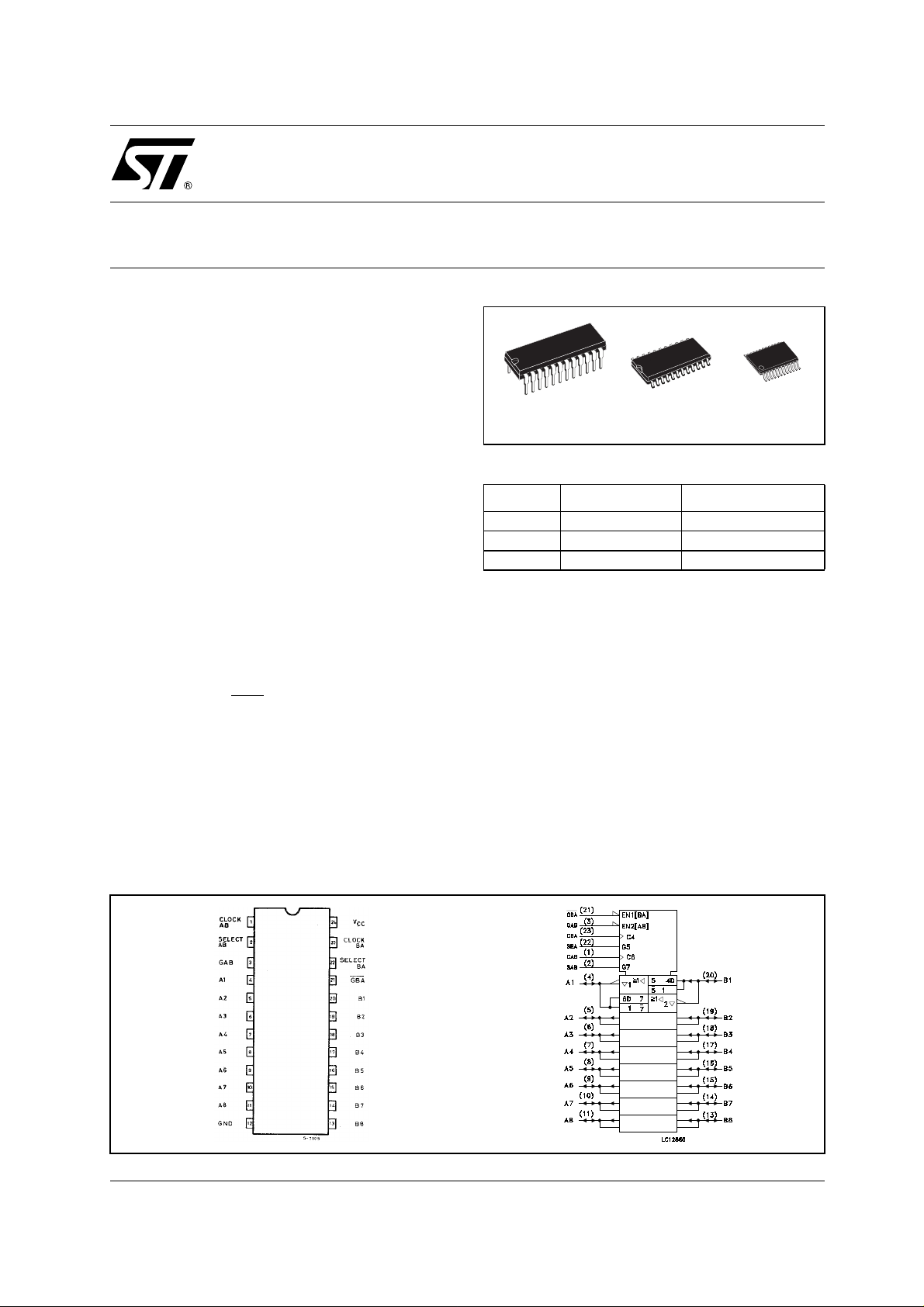
PIN CONNECTION AND IEC LOGIC SYMBOLS
1/15April 2003
M74HCT652
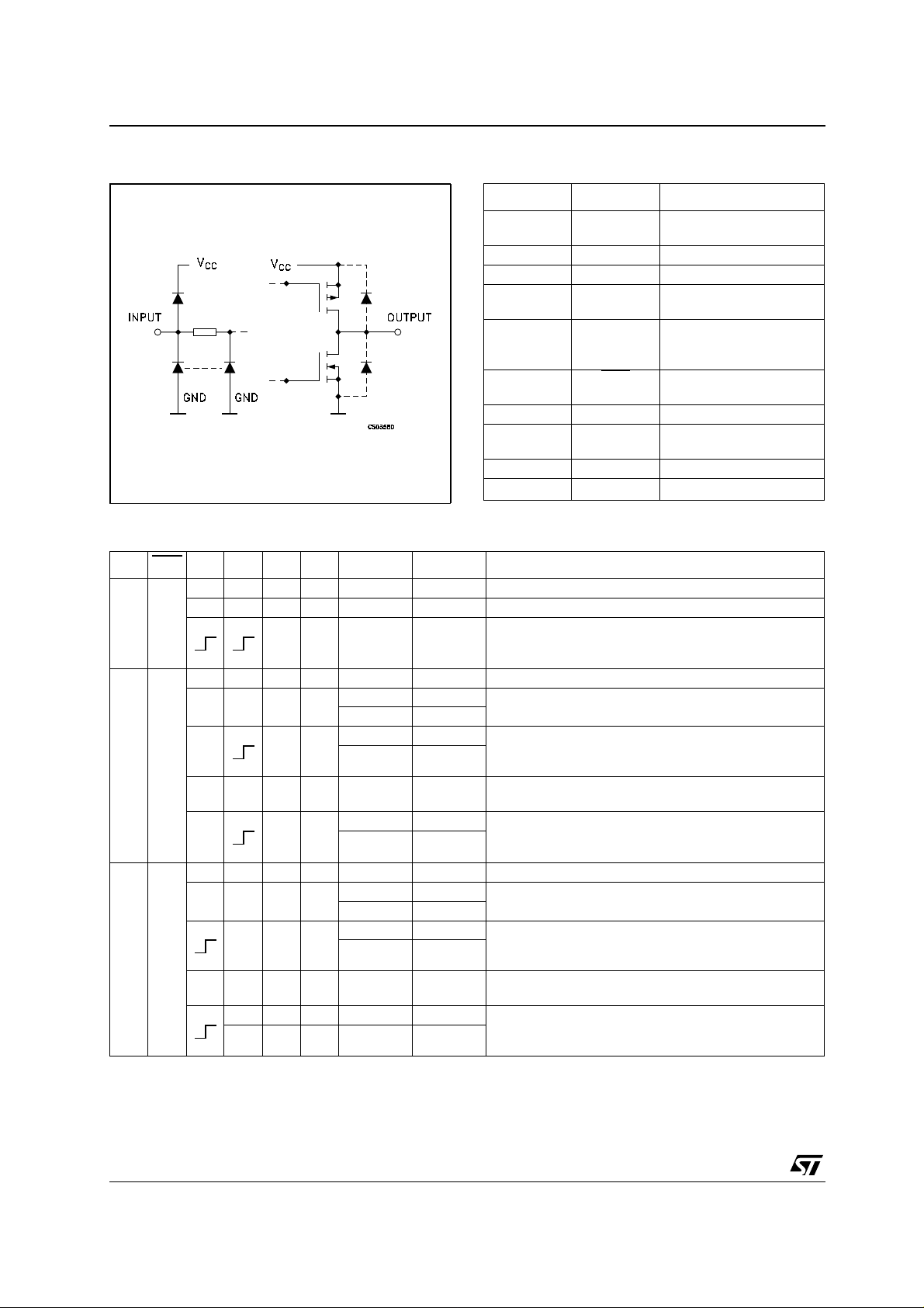
INPUT AND OUTPUT EQUIVALENT CIRCUIT PIN DESCRIPTION
PIN No SYMBOL NAME AND FUNCTION
1 CAB A to B Clock Input (LOW
2 SAB Select A to B Source Input
3 GAB Direction Control Input
4, 5, 6, 7, 8,
9, 10, 11
20, 19, 18,
17, 16, 15,
14, 13
21 GBA
22 SBA Select B to A Source Input
23 CBA B to A Clock Input (LOW
12 GND Ground (0V)
24 V
TRUTH TABLE
A1 to A8 A Data Inputs/Outputs
B1 to B8 B Data Inputs/Outputs
CC
to HIGH, Edge-Triggered)
Output Enable Input
(Active LOW)
to HIGH, Edge Triggered)
Positive Supply Voltage
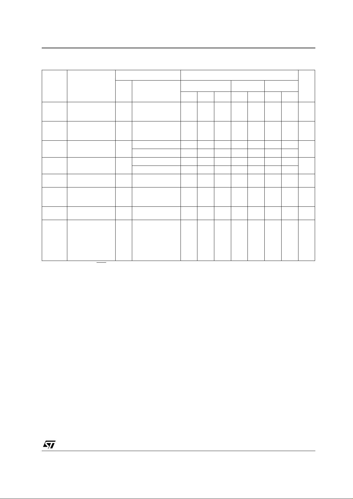
GAB GBA CAB CBA SAB SBA A B FUNCTION
INPUTS INPUTS Both the A bus and the B bus are inputs
LH
LL
HH
X X X X Z Z The Output functions of the A and B bus are disabled
X X INPUTS INPUTS
OUTPUTS INPUTS The A bus are outputs and the B bus are inputs
X* X X L
X* X L
X* X X H Qn X
X* X H
XX*L X
X* L X
XX*HX X Qn
X* H X L L The data at the A bus are stored to the internal flip-flop
X* H X H H
LL
HH
L L The data at the B bus are displayed at the A bus. The
HH
L L The data at the B bus are stored to the internal flip-flop
HH
INPUTS OUTPUTS The A bus are inputs and the B bus are outputs.
LL
HH
L L The data at the A bus are displayed at the B bus. The
HH
Both the A and B bus are used for inputs to the internal
flip-flops. Data at the bus will be stored on low to high
transition of the clock inputs.
The data at the B bus are displayed at the A bus
data of the B bus are stored to internal flip-flop on low
to high transition of the clock pulse
The data stored to the internal flip-flop are displayed at
the A bus.
on low to high transition of the clock pulse. The states
of the internal flip-flops output directly to the A bus.
The data at the A bus are displayed at the B bus
data of the A bus are stored to the internal flip-flop on
low to high transition of the clock pulse.
The data stored to the internal flip-flops are displayed
at the B bus
on low to high transition of the clock pulse. The states
of the internal flip-flops output directly to the B bus.
2/15
M74HCT652
GAB GBA
HL
X : Don’t Care
Z : High Impedance
Qn : The data stored to the internal flip-flops by mo st recent low to hi gh transition of the clock inputs
* : The data at the A and B bus will be stored to the internal flip-flops on every low to high transition of the clock inputs.
CAB CBA SAB SBA A B FUNCTION
OUTPUTS OUTPUTS
XXHH Qn Qn
H H Qn Qn
The data stored to the internal flip-flops are displayed
at the A and B bus respectively.
The output at the A bus are displayed at the B bus, the
output at the B bus are displayed at the A bus respectively
LOGIC DIAGRAM
TIMING CHART
3/15
M74HCT652
ABSOLUTE MAXIMUM RATINGS
Symbol Parameter Value Unit
V
V
V
I
I
OK
I
or I
I
CC
P
T
T
Absolute Maximum Ratings are those values beyond which damage to the device may occur. Functional operation under these conditions is
not implied
(*) 500mW at 65
RECOMMENDED OPERATING CONDITIONS
Symbol Parameter Value Unit
V
V
V
T
t
r
Supply Voltage
CC
DC Input Voltage -0.5 to VCC + 0.5
I
DC Output Voltage -0.5 to VCC + 0.5
O
DC Input Diode Current
IK
DC Output Diode Current
DC Output Current
O
DC VCC or Ground Current
GND
Power Dissipation
D
Storage Temperature
stg
Lead Temperature (10 sec)
L
°C; derate to 300mW by 10m W/°C from 65°C to 85°C
Supply Voltage
CC
Input Voltage 0 to V
I
Output Voltage 0 to V
O
Operating Temperature
op
, t
Input Rise and Fall Time (VCC = 4.5 to 5.5V)
f
-0.5 to +7 V
± 20 mA
± 20 mA
± 35 mA
± 70 mA
500(*) mW
-65 to +150 °C
300 °C
4.5 to 5.5 V
CC
CC
-55 to 125 °C
0 to 500 ns
V
V
V
V
4/15
DC SPECIFICATIONS
Test Condition Value
Symbol Parameter
V
V
V
High Level Input
IH
Voltage
V
Low Level Input
IL
Voltage
High Level Output
OH
Voltage
Low Level Output
OL
Voltage
Input Leakage
I
I
Current
I
High Impedance
OZ
Output Leakage
Current
Quiescent Supply
I
CC
Current
∆ I
Additional Worst
CC
Case Supply
Current
(*) Applicable Only to GAB, GBA, CAB, CBA, SAB, SBA Input
V
CC
(V)
4.5
to
5.5
4.5
to
5.5
4.5
4.5
5.5
5.5
5.5
IO=-20 µA
I
=-6.0 mA
O
IO=20 µA
I
=6.0 mA
O
= VCC or GND
V
I
= VIH or V
V
I
VO = VCC or GND
V
= VCC or GND
I
5.5 Per Input pin
= 0.5V or
V
I
V
= 2.4V
I
Other Inputs at
VCC or GND
I
= 0
O
= 25°C
T
A
-40 to 85°C -55 to 125°C
Min. Typ. Max. Min. Max. Min. Max.
2.0 2.0 2.0 V
0.8 0.8 0.8 V
4.4 4.5 4.4 4.4
4.18 4.31 4.13 4.10
0.0 0.1 0.1 0.1
0.17 0.26 0.33 0.40
± 0.1 ± 1 ± 1 µA
IL
± 0.5 ± 5 ± 10 µA
44080µA
2.0 2.9 3.0 mA
M74HCT652
Unit
V
V
5/15

M74HCT652
AC ELECTRICAL CHARACTERISTICS (CL = 50 pF, Input tr = tf = 6ns)
Test Condition Value
= 25°C
Symbol Parameter
t
TLH tTHL
t
PLH tPHL
t
PLH tPHL
Output Transition
Time
Propagation Delay
Time (BUS - BUS)
Propagation Delay
Time
(CLOCK - BUS)
t
PLH tPHL
Propagation Delay
Time
(SELECT - BUS)
t
PZL tPZH
High Impedance
Output Enable
Time
t
PLZ tPHZ
High Impedance
Output Disable
Time
f
t
W(H)
t
MAX
W(L)
t
s
t
h
Maximum Clock
Frequency
Minimum Pulse
Width
Minimum Set-Up
Time
Minimum Hold
Time
V
C
CC
(V)
L
(pF)
4.5 50 7 12 15 ns
4.5 50 20 30 38
4.5 150 25 38 48
4.5 50 29 44 55
4.5 150 34 52 65
4.5 50 24 34 43
4.5 150 29 42 53
R
4.5 50
4.5 150
4.5 50
= 1 KΩ
L
R
= 1 KΩ
L
R
= 1 KΩ
L
4.5 50 31 55 25 MHz
4.5 50 8 15 19 ns
4.5 50 3 10 13 ns
4.5 50 5 5 ns
T
A
Min. Typ. Max. Min. Max. Min. Max.
22 33 41
27 41 51
24 35 44 ns
-40 to 85°C -55 to 125°C
Unit
ns
ns
ns
ns
CAPACITIVE CHARACTERISTICS
Test Condition Value
= 25°C
Symbol Parameter
C
C
C
Input Capacitance
IN
Bus Terminal
I/O
Capacitance
Power Dissipation
PD
Capacitance (note
V
CC
(V)
T
A
Min. Typ. Max. Min. Max. Min. Max.
510 10 10pF
13 pF
39 pF
1)
1) CPD is defined as the value of the IC’s internal equivalent capacitance which is calculated from the operating current consumption without
load. (R ef er to Test Circui t). Averag e operating cu rrent can be ob ta i ned by the following equat io n. I
channel)
-40 to 85°C -55 to 125°C
= CPD x VCC x fIN + ICC/8 (per
CC(opr)
Unit
6/15

TEST CIRCUIT
TEST SWITCH
t
, t
PLH
PHL
, t
t
PZL
PLZ
t
, t
PZH
PHZ
CL = 50pF/150p F or equivalen t (includes ji g and probe capa citance)
R
= 1KΩ or equivalent
1
R
= Z
of pulse generator (typically 50Ω)
T
OUT
M74HCT652
Open
V
CC
GND
WAVEFORM 1 : PROPAGATION DELAY TIME(f=1MHz; 50% duty cycle)
7/15

M74HCT652
WAVEFORM 2 : MINIMUM PULSE WIDTH, PROPAGATION DELAY (f=1MHz; 50% duty cycle)
WAVEFORM 3 : MINIMUM SETUP AND HOLD TIME ((f=1MHz; 50% duty cycle)
8/15

WAVEFORM 4 : OUTPUT ENABLE AND DISABLE TIME (f=1MHz; 50% duty cycle)
M74HCT652
WAVEFORM 5 : OUTPUT ENABLE AND DISABLE TIME(f=1MHz; 50% duty cycle)
9/15

M74HCT652
Plastic DIP-24 (0.25) MECHANICAL DATA
mm. inch
DIM.
MIN. TYP MAX. MIN. TYP. MAX.
A 4.32 0.170
A1 0.38 0.015
A2 3.3 0.130
B 0.41 0.46 0.51 0.016 0.018 0.020
B1 1.40 1.52 1.65 0.055 0.060 0.065
c 0.20 0.25 0.30 0.008 0.010 0.012
D 31.62 31.75 31.88 1.245 1.250 1.255
E 7.62 8.26 0.300 0.325
E1 6.35 6.60 6.86 0.250 0.260 0.270
e 2.54 0.100
E1 7.62 0.300
L 3.18 3.43 0.125 0.135
M 0˚ 15˚ 0˚ 15˚
E
E1
A2
A1
LA
B eB1
D
24
1
13
12
Stand-off
e1
c
.015
0,38
Gage Plane
10/15
M
0034965/D

SO-24 MECHANICAL DATA
M74HCT652
DIM.
MIN. TYP MAX. MIN. TYP. MAX.
A 2.65 0.104
a1 0.1 0.2 0.004 0.008
a2 2.45 0.096
b 0.35 0.49 0.014 0.019
b1 0.23 0.32 0.009 0.012
C 0.5 0.020
c1 45˚ (typ.)
D 15.20 15.60 0.598 0. 614
E 10.00 10.65 0.393 0.419
e 1.27 0.050
e3 13.97 0.550
F 7.40 7.60 0. 291 0. 300
L 0.50 1.27 0.020 0.050
S ˚ (max.)
mm. inch
8
A
a2
b
e
e3
D
24 13
F
112
L
a1
c1
b1
C
s
E
PO13T
11/15

M74HCT652
TSSOP24 MECHANICAL DATA
mm. inch
DIM.
MIN. TYP MAX. MIN. TYP. MAX.
A 1.1 0.043
A1 0.05 0.15 0.002 0.006
A2 0.9 0.035
b 0.19 0.30 0.0075 0.0118
c 0.09 0.20 0.0035 0.0079
D 7.7 7.9 0.303 0.311
E 6.25 6.5 0.246 0.256
E1 4.3 4.5 0.169 0.177
e 0.65 BSC 0.0256 BSC
K0˚ 8˚0˚ 8˚
L 0.50 0.70 0.020 0.028
A2
A
A1
b
e
D
K
c
E1
L
E
PIN 1 IDENTIFICATION
12/15
1
7047476A

M74HCT652
Tape & Reel SO-24 MECHANICAL DATA
mm. inch
DIM.
MIN. TYP MAX. MIN. TYP. MAX.
A 330 12.992
C 12.8 13.2 0.504 0.519
D 20.2 0.795
N 60 2.362
T 30.4 1.197
Ao 10.8 11.0 0.425 0.433
Bo 15.7 15.9 0.618 0.626
Ko 2.9 3.1 0.114 0.122
Po 3.9 4.1 0.153 0.161
P 11.9 12.1 0.468 0.476
13/15

M74HCT652
Tape & Reel TSSOP24 MECHANICAL DATA
mm. inch
DIM.
MIN. TYP MAX. MIN. TYP. MAX.
A 330 12.992
C 12.8 13.2 0.504 0.519
D 20.2 0.795
N 60 2.362
T 22.4 0.882
Ao 6.8 7 0.268 0.276
Bo 8.2 8.4 0.323 0.331
Ko 1.7 1.9 0.067 0.075
Po 3.9 4.1 0.153 0.161
P 11.9 12.1 0.468 0.476
14/15

M74HCT652
Information furnished is believed to be accurate and reliable. However, STMicroelectronics assumes no responsibility for the
consequences of use o f suc h inf ormat ion n or f or an y infr ingeme nt of paten ts or oth er ri gh ts of third part ies whic h may resul t f rom
its use. No license is granted by implication or otherwise under any patent or patent rights of STMicroelectronics. Specifications
mentioned in this publication are subject to change without notice. This publication supersedes and replaces all information
previously supplied. STMicroelectronics products are not authorized for use as critical components in life support devices or
systems without express written approval of STMicroelectronics.
Australia - Brazil - Canada - China - Finland - France - Germany - Hong Kong - India - Israel - Italy - Japan - Malaysia - Malta - Morocco
© The ST logo is a registered trademark of STMicroelectronics
© 2003 STMicroelectronics - Printed in Italy - All Rights Reserved
STMicroelectronics GROUP OF COMPANIES
Singapore - Spain - Sweden - Switzerland - United Kingdom - United States.
© http://www.st.com
15/15
 Loading...