

M74HCT640
OCTAL BUS TRANSCEIVER
WITH 3 STATE OUTPUTS (INVERTED)
■ HIGH SPEED:
t
= 13ns (TYP.) at VCC = 4.5V
PD
■ LOW POWER DISSIPATION:
I
= 4µA(MAX.) at TA=25°C
CC
■ COMPA TIBLE WITH TTL OUTPUTS :
V
= 2V (MIN.) VIL = 0.8V (MAX)
IH
■ SYMMETRICAL OUTPUT IMPEDANCE:
|I
| = IOL = 6mA (MIN)
OH
■ BALANCED PROPAGATION DELAYS:
t
≅ t
PHL
PLH
■ PIN AND FUNCTION COMPATIBLE WITH
74 SERIES 640
DESCRIPTION
The M74HCT640 is an advanced high-speed
CMOS OCTAL BUS TRANSCEIVER (3-STATE)
fabricated with silicon gate C
2
MOS technology.
This IC is intended for two-way asynchronous
communication between data buses, and the
direction of data transmission is determined by
DIR input. The enable input G
can be used to
disable the device so that the buses are effectively
isolated.
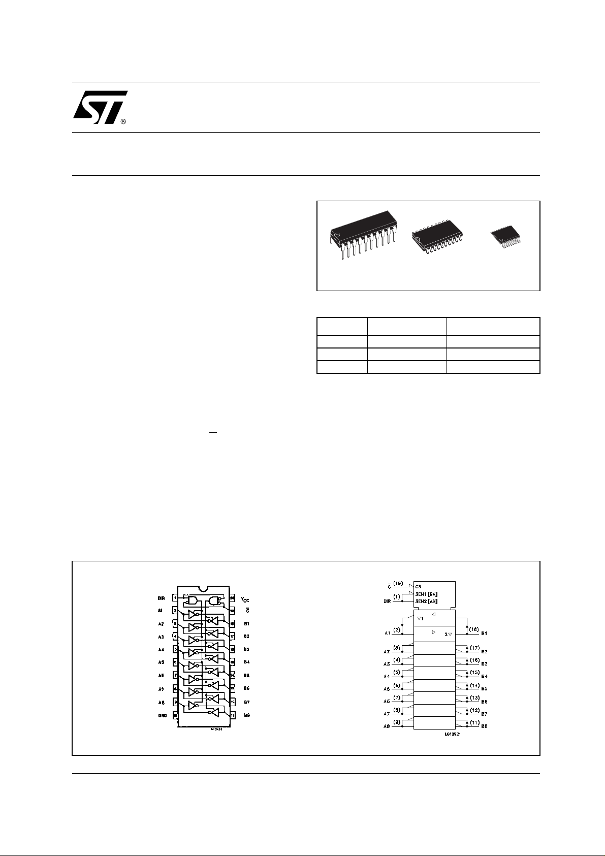
TSSOPDIP SOP
ORDER CODES
PACKAGE TUBE T & R
DIP M74HCT640B1R
SOP M74HCT640M1R M74HCT640RM13TR
TSSOP M74HCT640TTR
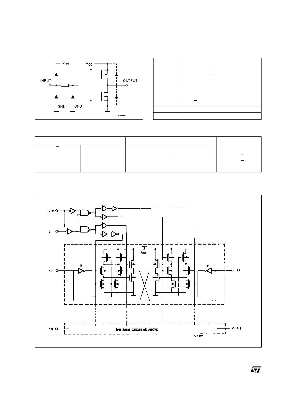
All inputs are equipped with protection circuits
against static discharge and transient excess
voltage.
All floating bus terminals during High Z State must
be held HIGH or LOW.
PIN CONNECTION AND IEC LOGIC SYMBOLS
1/11August 2001
M74HCT640
INPUT AND OUTPUT EQUIVALENT CIRCUIT PIN DESCRIPTION
PIN No SYMBOL NAME AND FUNCTION
1 DIR Directional Control
2, 3, 4, 5, 6,
7, 8, 9
18, 17, 16,
15, 14, 13,
12, 11
19 G
10 GND Ground (0V)
20 V
TRUTH TABLE
A1 to A8 Data Inputs/Outputs
B1 to B8 Data Inputs/Outputs
CC
Output Enable Input
Positive Supply Voltage
INPUTS FUNCTION
G
L L OUTPUT INPUT A = B
L H INPUT OUTPUT B = A
HXZZZ
X : Don’t Care
Z : High Impedance
LOGIC DIAGRAM
DIR A BUS B BUS
OUTPUT
This log i c diagram has not be used to esti m ate propagation delays
2/11

M74HCT640
ABSOLUTE MAXIMUM RATINGS
Symbol Parameter Value Unit
V
V
V
I
I
OK
I
I
or I
CC
P
T
T
Absolute Maximum Ratings are those values beyond which damage to the device may occur. Functional operation under these conditions is
not implied
(*) 500mW at 65
RECOMMENDED OPERATING CONDITIONS
Symbol Parameter Value Unit
V
V
V
T
t
r
Supply Voltage
CC
DC Input Voltage -0.5 to VCC + 0.5
I
DC Output Voltage -0.5 to VCC + 0.5
O
DC Input Diode Current
IK
DC Output Diode Current
DC Output Current
O
DC VCC or Ground Current
GND
Power Dissipation
D
Storage Temperature
stg
Lead Temperature (10 sec)
L
°C; derate to 300mW by 10mW/°C from 65°C to 85°C
Supply Voltage
CC
Input Voltage 0 to V
I
Output Voltage 0 to V
O
Operating Temperature
op
, t
Input Rise and Fall Time (VCC = 4.5 to 5.5V)
f
-0.5 to +7 V
± 20 mA
± 20 mA
± 35 mA
± 70 mA
500(*) mW
-65 to +150 °C
300 °C
4.5 to 5.5 V
CC
CC
-55 to 125 °C
0 to 500 ns
V
V
V
V
3/11

M74HCT640
DC SPECIFICATIONS
Symbol Parameter
V
V
V
V
I
I
∆ I
High Level Input
IH
Voltage
Low Level Input
IL
Voltage
High Level Output
OH
Voltage
Low Level Output
OL
Voltage
I
Input Leakage
I
Current
High Impedance
OZ
Output Leakage
Current
Quiescent Supply
CC
Current
Additional Worst
CC
Case Supply
Current
Test Condition Value
T
= 25°C
V
(V)
CC
A
Min. Typ. Max. Min. Max. Min. Max.
4.5
to
2.0 2.0 2.0 V
5.5
4.5
to
0.8 0.8 0.8 V
5.5
4.5
4.5
5.5
5.5
5.5
IO=-20 µA
I
=-6.0 mA
O
IO=20 µA
I
=6.0 mA
O
= VCC or GND
V
I
= VIH or V
V
I
VO = VCC or GND
= VCC or GND
V
I
5.5 Per Input pin
= 0.5V or
V
I
V
= 2.4V
I
4.4 4.5 4.4 4.4
4.18 4.31 4.13 4.10
0.0 0.1 0.1 0.1
0.17 0.26 0.33 0.40
± 0.1 ± 1 ± 1 µA
IL
± 0.5 ± 5 ± 10 µA
2.0 2.9 3.0 mA
Other Inputs at
V
or GND
CC
I
= 0
O
-40 to 85°C -55 to 125°C
Unit
V
V
44080µA
4/11
 Loading...