

M74HCT573
OCTAL D-TYPE LATCH
WITH 3 STATE OUTPUT NON INVERTING
■ HIGH SPEED:
t
= 21ns (TYP.) at VCC = 4.5V
PD
■ LOW POWER DISSIPATION:
I
= 4µA(MAX.) at TA=25°C
CC
■ COMPA TIBLE WITH TTL OUTPUTS :
V
= 2V (MIN.) VIL = 0.8V (MAX)
IH
■ BALANCED PROPAGATION DELAYS:
t
≅ t
PLH
■ SYMMETRICAL OUTPUT IMPEDANCE:
|I
OH
■ PIN AND FUNCTION COMPATIBLE WITH
PHL
| = IOL = 6mA (MIN)
74 SERIES 573
DESCRIPTION
The M74HCT573 is an high speed CMOS OCTAL
LATCH WITH 3-STATE OUTPUTS fabricated
with silicon gate C
2
MOS technology.
This 8-BIT D-Type la tches is controlled by a latc h
enable input (LE) and output enable input (OE
).
While the LE in put is held at a high level, the Q
outputs will follow the data input precisely. Wh en
the LE is taken low, the Q outputs will be latched
precisely at the logic level of D input data.
While the OE
input is at low level, the eight outputs
will be in a norm al logic state (high or low logic
level) and while OE
is at high level the outputs will
be in a high impedance state.
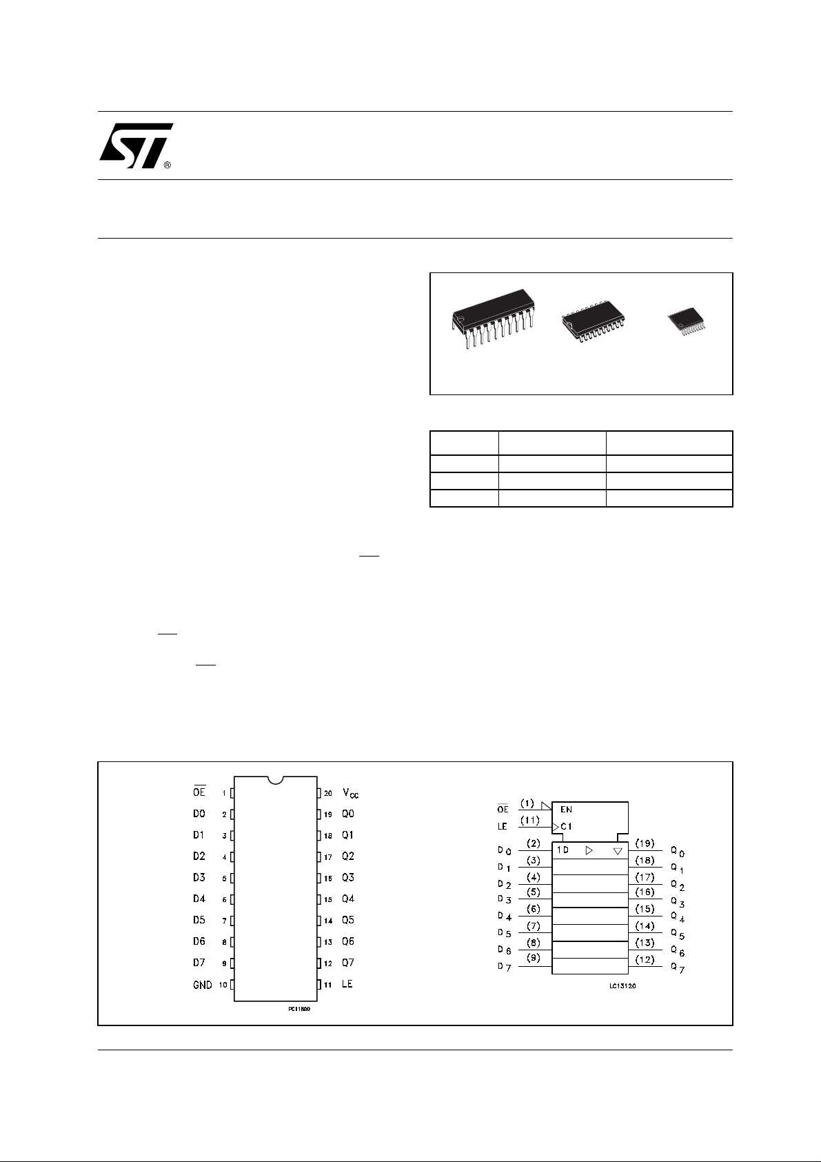
TSSOPDIP SOP
ORDER CODES
PACKAGE TUBE T & R
DIP M74HCT573B1R
SOP M74HCT573M1R M74HCT573RM13TR
TSSOP M74HCT573TTR
The 3-State output configuration and the wide
choice of outline make bus organized system
simple.
The M74HCT573 is designed to directly interface
2
HSC
MOS systems with TTL and NMOS
components.
All inputs are equipped with protection circuits
against static discharge and transient excess
voltage.
PIN CONNECTION AND IEC LOGIC SYMBOLS
1/11July 2001
M74HCT573
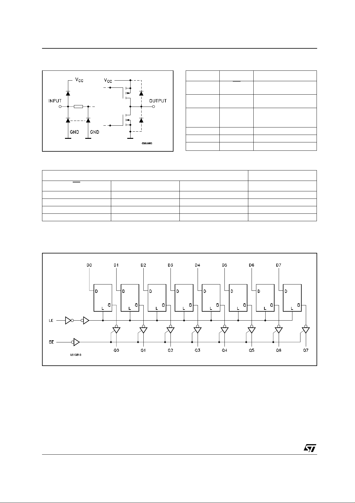
INPUT AND OUTPUT EQUIVALENT CIRCUIT PIN DESCRIPTION
PIN No SYMBOL NAME AND FUNCTION
1OE
2, 3, 4, 5, 6,
7, 8, 9
12, 13, 14,
15, 16, 17,
18, 19
11 LE Latch Enable Input
10 GND Ground (0V)
20 V
TRUTH TABLE
INPUTS OUTPUTS
D0 to D7 Data Inputs
Q0 to Q7 3 State Latch Outputs
CC
3 State Output Enable
Input (Active LOW)
Positive Supply Voltage
OE
HXXZ
L L X NO CHANGE (*)
LHLL
LHHH
X: Don’t Care
Z: High Impedance
(*): Q Outputs are lat ched at the time when the LE i nput is taken lo w l ogic level.
LE D Q
LOGIC DIAGRAM
2/11
M74HCT573
ABSOLUTE MAXIMUM RATINGS
Symbol Parameter Value Unit
V
V
V
I
I
OK
I
I
or I
CC
P
T
T
Absolute Maximum Ratings are those values beyond which damage to the device may occur. Functional operation under these conditions is
not implied
(*) 500mW at 65
RECOMMENDED OPERATING CONDITIONS
Symbol Parameter Value Unit
V
V
V
T
t
r
Supply Voltage
CC
DC Input Voltage -0.5 to VCC + 0.5
I
DC Output Voltage -0.5 to VCC + 0.5
O
DC Input Diode Current
IK
DC Output Diode Current
DC Output Current
O
DC VCC or Ground Current
GND
Power Dissipation
D
Storage Temperature
stg
Lead Temperature (10 sec)
L
°C; derate to 300mW by 10mW/°C from 65° C to 85°C
Supply Voltage
CC
Input Voltage 0 to V
I
Output Voltage 0 to V
O
Operating Temperature
op
, t
Input Rise and Fall Time (VCC = 4.5 to 5.5V)
f
-0.5 to +7 V
± 20 mA
± 20 mA
± 35 mA
± 70 mA
500(*) mW
-65 to +150 °C
300 °C
4.5 to 5.5 V
CC
CC
-55 to 125 °C
0 to 500 ns
V
V
V
V
3/11
M74HCT573
DC SPECIFICATIONS
Symbol Parameter
V
V
V
V
I
I
∆ I
High Level Input
IH
Voltage
Low Level Input
IL
Voltage
High Level Output
OH
Voltage
Low Level Output
OL
Voltage
I
Input Leakage
I
Current
High Impedance
OZ
Output Leakage
Current
Quiescent Supply
CC
Current
Additional Worst
CC
Case Supply
Current
Test Condition Value
T
= 25°C
V
CC
(V)
A
Min. Typ. Max. Min. Max. Min. Max.
4.5
to
2.0 2.0 2.0 V
5.5
4.5
to
0.8 0.8 0.8 V
5.5
4.5
4.5
5.5
5.5
5.5
IO=-20 µA
I
=-6.0 mA
O
IO=20 µA
I
=6.0 mA
O
= VCC or GND
V
I
= VIH or V
V
I
VO = VCC or GND
= VCC or GND
V
I
5.5 Per Input pin
= 0.5V or
V
I
V
= 2.4V
I
4.4 4.5 4.4 4.4
4.18 4.31 4.13 4.10
0.0 0.1 0.1 0.1
0.17 0.26 0.33 0.40
± 0.1 ± 1 ± 1 µA
IL
± 0.5 ± 5 ± 10 µA
2.0 2.9 3.0 mA
Other Inputs at
V
or GND
CC
-40 to 85°C -55 to 125°C
Unit
V
V
44080µA
AC ELECTRICAL CHARACTERISTICS (C
Test Condition Value
Symbol Parameter
t
TLH tTHL
t
PLH tPHL
t
PLH tPHL
t
PZL tPZH
t
PLZ tPHZ
t
W(L)
t
W(H)
Output Transition
Time
Propagation Delay
Time (LE - Q,Q
Propagation Delay
Time (D - Q,Q
Output Enable
Time
Output Disable
Time
Minimum Pulse
Width (LE)
Minimum Set-Up
t
s
Time
Minimum Hold
t
h
Time
)
V
C
(pF)
L
CC
(V)
4.5 50 7 12 15 18 ns
4.5 50 21 33 41 50
)
4.5 150 25 39 49 59
4.5 50 19 30 38 45
4.5 150 23 36 45 54
4.5 50
4.5 150 23 36 45 54
4.5 50
4.5 50 7 15 19 22 ns
4.5 50 4 10 13 15 ns
4.5 50 5 5 5 ns
= 50 pF, Input tr = tf = 6ns)
L
= 25°C
T
A
Min. Typ. Max. Min. Max. Min. Max.
= 1 KΩ
R
L
= 1 KΩ
R
L
19 30 38 45
18 25 31 38 ns
-40 to 85°C -55 to 125°C
Unit
ns
ns
ns
4/11
 Loading...