

ST M74HCT374 User Manual
M74HCT374
OCTAL D-TYPE FLIP FLOP
WITH 3 STATE OUTPUT NON INVERTING
■ HIGH SPEED:
f
= 50 MHz (TYP.) at VCC = 4.5V
MAX
■ LOW POWER DISSIPATION:
I
= 4µA(MAX.) at TA=25°C
CC
■ COMPAT I B LE WITH TT L OUTPUTS :
V
= 2V (MIN.) VIL = 0.8V (MAX)
IH
■ BALANCED PROPAGATION DELAYS:
t
≅ t
PLH
■ SYMMETRICAL OUTPUT IMPEDANCE:
|I
OH
■ PIN AND FUNCTION COMPATIBLE WITH
PHL
| = IOL = 6mA (MIN)
74 SERIES 374
DESCRIPTION
The M74HCT374 is an high speed CMOS OCTAL
D-TYPE FLIP FLOP WITH 3-STATE OUTPUTS
NON INVERTING fabricated with silicon gate
2
C
MOS technology.
This 8 bit D-TYPE FLIP FLOP is con trolled by a
clock input (CK) and an o utpu t enable input (OE
On the positive transition of the clock, the Q
outputs will be set to the logic state that were
setup at the D inputs.
While the OE
input is at low level, the eight outputs
will be in a norm al logic state (high or low logic
level) and while OE
is at high level the outputs will
be in a high impedance state.
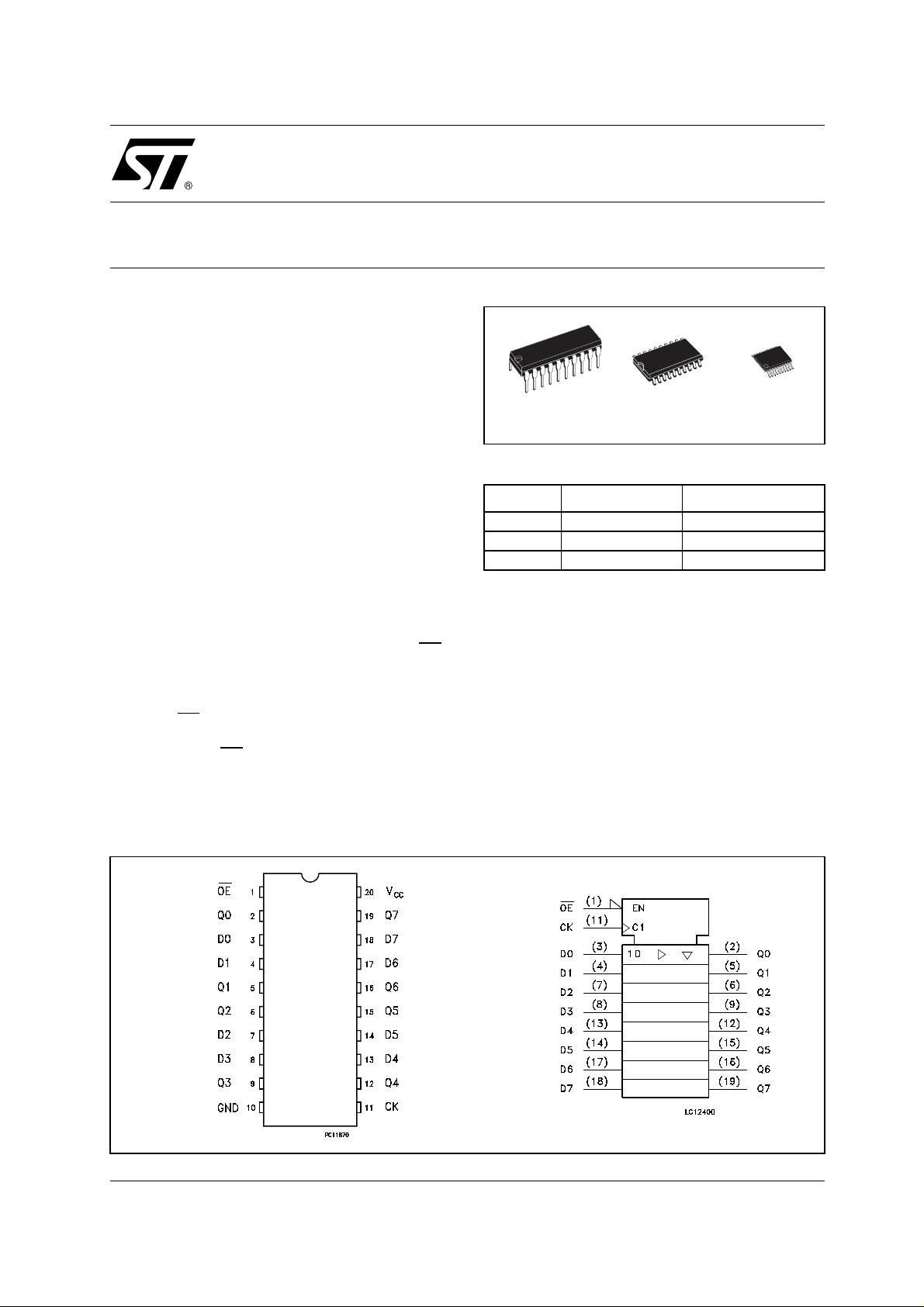
ORDER CODES
PACKAGE TUBE T & R
DIP M74HCT374B1R
SOP M74HCT374M1R M74HCT374RM13TR
TSSOP M74HCT374TTR
The output control does not affect the internal
operation of flip-flops; that is, the old data can be
retained or the new data can be entered even
).
while the outputs are off.
The M74HCT374 is designed to directly interface
2
HSC
MOS systems with TTL and NMOS
components.
All inputs are equipped with protection circuits
against static discharge and transient excess
voltage.
TSSOPDIP SOP
PIN CONNECTION AND IEC LOGIC SYMBOLS
1/11July 2001
M74HCT374
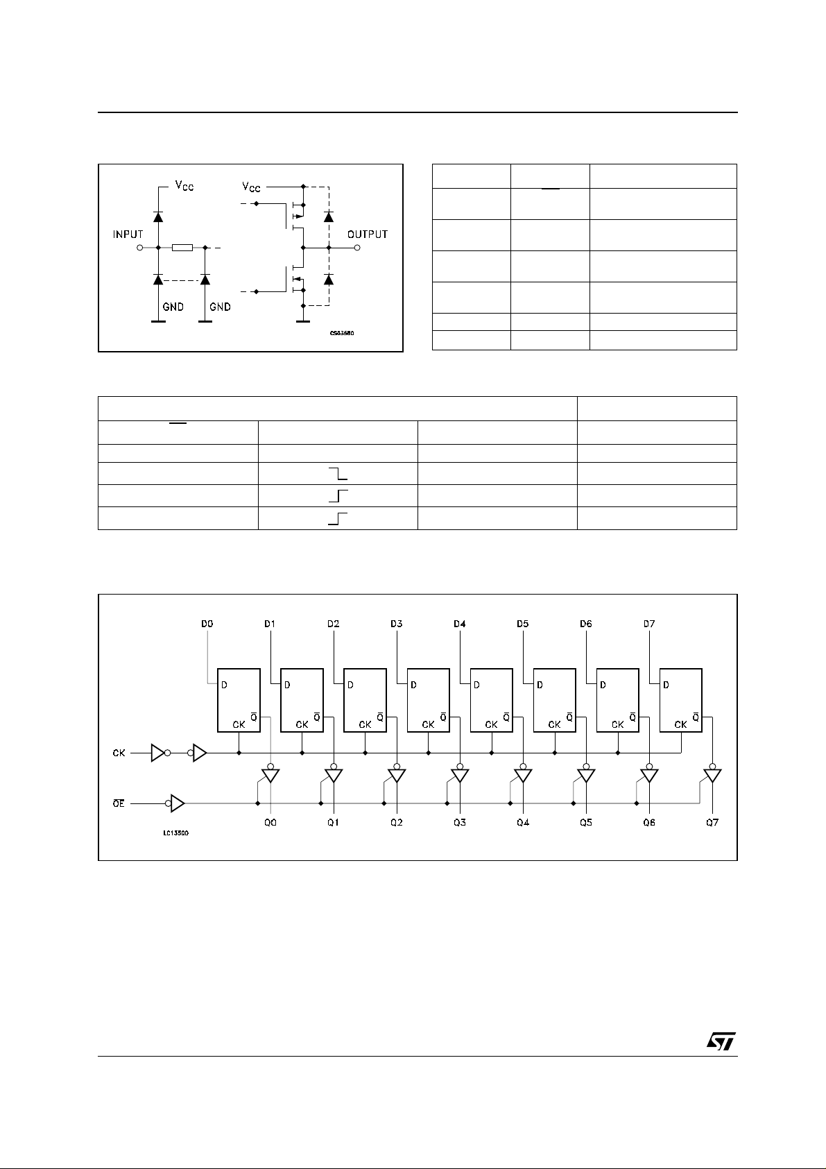
INPUT AND OUTPUT EQUIVALENT CIRCUIT PIN DESCRIPTION
PIN No SYMBOL NAME AND FUNCTION
1OE
2, 5, 6, 9, 12,
15, 16, 19
3, 4, 7, 8, 13,
14, 17, 18
11 CK Clock Input (LOW to
10 GND Ground (0V)
20 V
TRUTH TABLE
INPUTS OUTPUT
Q0 to Q7 3 State Outputs
D0 to D7 Data Inputs
CC
3 State Output Enable
Input (Active LOW)
HIGH, edge triggered)
Positive Supply Voltage
OE
HXXZ
L X NO CHANGE
LLL
LHH
X: Don’t Care
Z: High Impedance
LOGIC DIAGRAM
CK D Q
This log i c diagram has not be used to e st i m ate propagation dela ys
2/11
M74HCT374
ABSOLUTE MAXIMUM RATINGS
Symbol Parameter Value Unit
V
V
V
I
I
OK
I
I
or I
CC
P
T
T
Absolute Maximum Ratings are those values beyond which damage to the device may occur. Functional operation under these conditions is
not implied
(*) 500mW at 65
RECOMMENDED OPERATING CONDITIONS
Symbol Parameter Value Unit
V
V
V
T
t
r
Supply Voltage
CC
DC Input Voltage -0.5 to VCC + 0.5
I
DC Output Voltage -0.5 to VCC + 0.5
O
DC Input Diode Current
IK
DC Output Diode Current
DC Output Current
O
DC VCC or Ground Current
GND
Power Dissipation
D
Storage Temperature
stg
Lead Temperature (10 sec)
L
°C; derate to 300mW by 10mW/°C from 65° C to 85°C
Supply Voltage
CC
Input Voltage 0 to V
I
Output Voltage 0 to V
O
Operating Temperature
op
, t
Input Rise and Fall Time (VCC = 4.5 to 5.5V)
f
-0.5 to +7 V
± 20 mA
± 20 mA
± 35 mA
± 70 mA
500(*) mW
-65 to +150 °C
300 °C
4.5 to 5.5 V
CC
CC
-55 to 125 °C
0 to 500 ns
V
V
V
V
3/11
M74HCT374
DC SPECIFICATION
Symbol Parameter
V
V
V
V
I
I
∆ I
High Level Input
IH
Voltage
Low Level Input
IL
Voltage
High Level Output
OH
Voltage
Low Level Output
OL
Voltage
I
Input Leakage
I
Current
High Impedance
OZ
Output Leakage
Current
Quiescent Supply
CC
Current
Additional Worst
CC
Case Supply
Current
Test Condition Value
T
= 25°C
V
CC
(V)
A
Min. Typ. Max. Min. Max. Min. Max.
4.5
to
2.0 2.0 2.0 V
5.5
4.5
to
0.8 0.8 0.8 V
5.5
4.5
4.5
5.5
5.5
5.5
IO=-20 µA
I
=-6.0 mA
O
IO=20 µA
I
=6.0 mA
O
= VCC or GND
V
I
= VIH or V
V
I
VO = VCC or GND
= VCC or GND
V
I
5.5 Per Input pin
= 0.5V or
V
I
V
= 2.4V
I
4.4 4.5 4.4 4.4
4.18 4.31 4.13 4.10
0.0 0.1 0.1 0.1
0.17 0.26 0.33 0.40
± 0.1 ± 1 ± 1 µA
IL
± 0.5 ± 5 ± 10 µA
2.0 2.9 3.0 mA
Other Inputs at
V
or GND
CC
I
= 0
O
-40 to 85°C -55 to 125°C
Unit
V
V
44080µA
AC ELECTRICAL CHARACTERISTICS (C
Test Condition Value
Symbol Parameter
t
TLH tTHL
t
PLH tPHL
t
PZL tPZH
t
PLZ tPHZ
f
MAX
t
W(L)
t
W(H)
Output Transition
Time
Propagation Delay
Time (CLOCK-Q,Q
Output Enable
Time
Output Disable
Time
Maximum Clock
Frequency
Minimum Pulse
Width (CLOCK)
t
Minimum Set-Up
s
Time
Minimum Hold
t
h
Time
)
C
(pF)
L
V
CC
(V)
4.5 50 7 12 15 18 ns
4.5 50 20 30 38 45
4.5 150 25 38 48 57
4.5 50
4.5 150 25 38 48 57
4.5 50
4.5 50 31 50 25 21 MHz
4.5 50 15 19 23 ns
4.5 50 15 19 23 ns
4.5 50 0 0 0 ns
= 50 pF, Input tr = tf = 6ns)
L
= 25°C
T
A
Min. Typ. Max. Min. Max. Min. Max.
= 1 KΩ
R
L
= 1 KΩ
R
L
17 30 38 45
16 28 35 42 ns
-40 to 85°C -55 to 125°C
Unit
ns
ns
4/11
 Loading...