

M74HCT132
QUAD 2-INPUT SCHMITT NAND GATE
■ HIGH SPEED:
t
= 19ns (TYP.) at V
PD
■ LOW POWER DISSIPATION:
= 1µA(MAX.) at TA=25°C
I
CC
■ HIGH NOISE IMMUNITY :
V
= 0.7V (TYP) at Vcc = 4.5V
H
■ BALANCED PROPAGATION DELAYS:
t
≅ t
PLH
■ SYMMETRICAL OUTPUT IMPEDANCE:
|I
OH
■ PIN AND FUNCTION COMPATIBLE WITH
PHL
| = IOL = 4mA (MIN)
CC
= 4.5V
74 SERIES 132
DESCRIPTION
The M74HCT132 is an high s peed CM OS QUA D
2-INPUT SCHMITT NAND GATE fabricated with
silicon gate C
2
MOS technology.
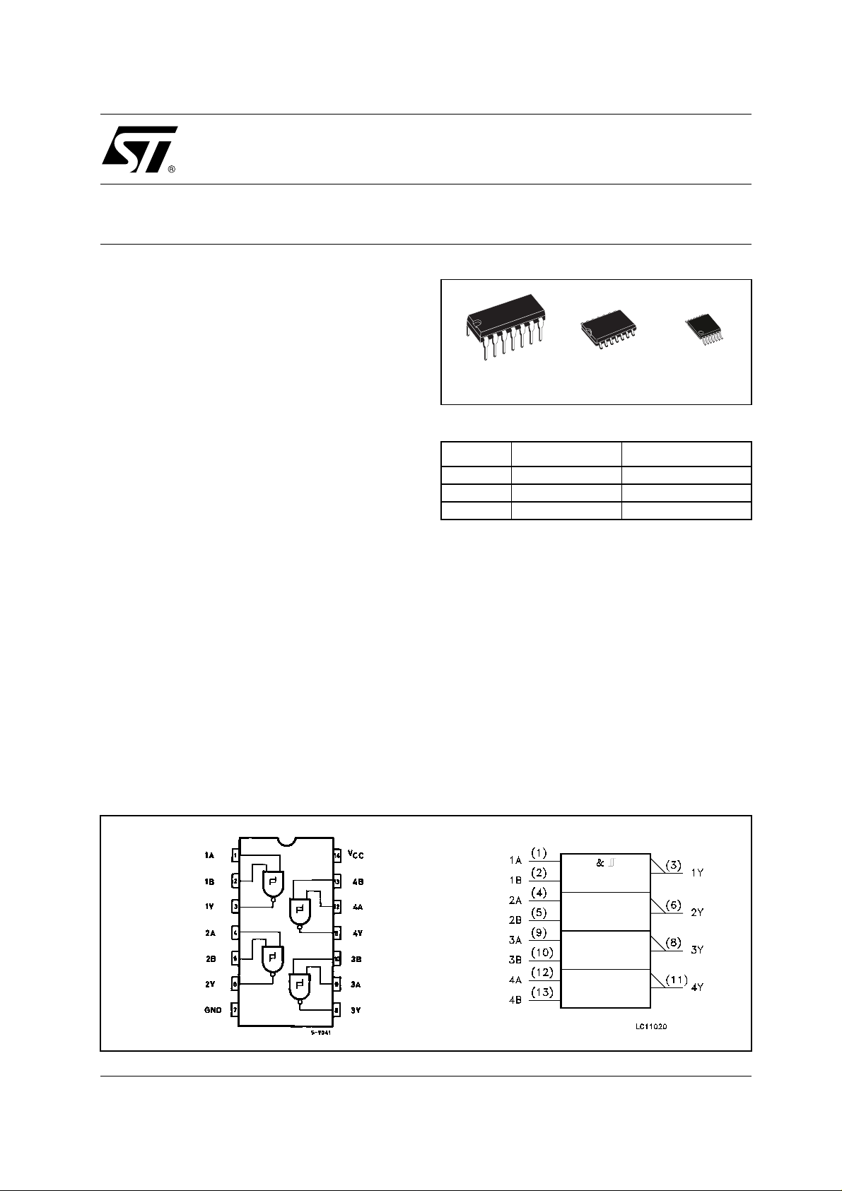
Pin configuration and function are the same as
those of the M74HCT00. The hysteresis
characteristics (around 20% V
) of all inputs allow
cc
slowly changing input signals to be transformed
into sharply defined jitter-free output signals.
TSSOPDIP SOP
ORDER CODES
PACKAGE TUBE T & R
DIP M74HCT132B1R
SOP M74HCT132M1R M74HCT132RM13TR
TSSOP M74HCT132TTR
The M74HCT132 is designed to directly interface
2
HSC
MOS systems with TTL and NMOS
components.
All inputs are equipped with protection circuits
against static discharge and transient excess
voltage.
PIN CONNECTION AND IEC LOGIC SYMBOLS
1/8July 2001
M74HCT132
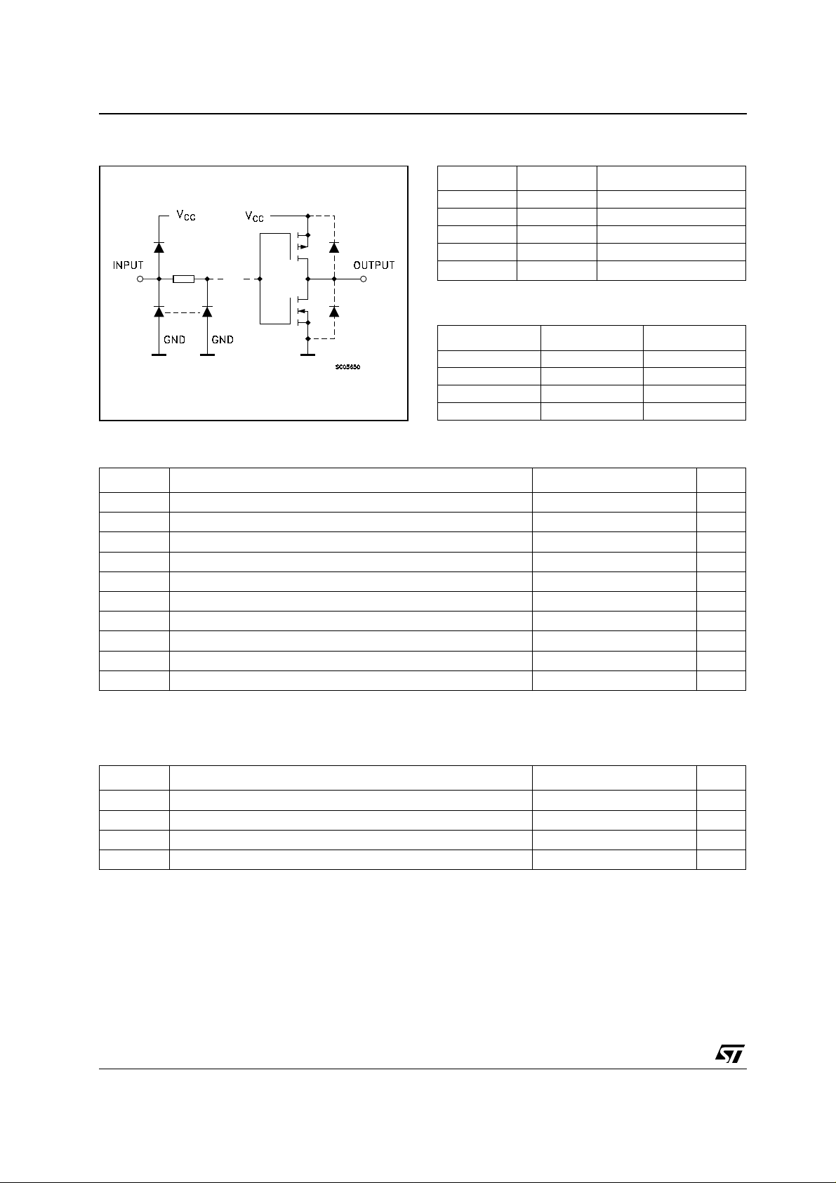
INPUT AND OUTPUT EQUIVALENT CIRCUIT PIN DESCRIPTION
PIN No SYMBOL NAME AND FUNCTION
1, 4, 9, 12 1A to 4A Data Inputs
2, 5, 10, 13 1B to 4B Data Inputs
3, 6, 8, 11 1Y to 4Y Data Outputs
7 GND Ground (0V)
14
V
CC
TRUTH TABLE
ABY
LLH
LHH
HLH
HHL
ABSOLUTE MAXIMUM RATINGS
Symbol Parameter Value Unit
V
V
V
I
I
OK
I
I
or I
CC
P
T
T
Absolute Maximum Ratings are those values beyond which damage to the device may occur. Functional operation under these conditions is
not implied
(*) 500mW at 65
Supply Voltage
CC
DC Input Voltage -0.5 to VCC + 0.5
I
DC Output Voltage -0.5 to VCC + 0.5
O
DC Input Diode Current
IK
DC Output Diode Current
DC Output Current
O
DC VCC or Ground Current
GND
Power Dissipation
D
Storage Temperature
stg
Lead Temperature (10 sec)
L
°C; derate to 300mW by 10mW/°C from 65 °C to 85°C
Positive Supply Voltage
-0.5 to +7 V
V
V
± 20 mA
± 20 mA
± 25 mA
± 50 mA
500(*) mW
-65 to +150 °C
300 °C
RECOMMENDED OPERATING CONDITIONS
Symbol Parameter Value Unit
V
V
V
T
2/8
Supply Voltage
CC
Input Voltage 0 to V
I
Output Voltage 0 to V
O
Operating Temperature
op
4.5 to 5.5 V
CC
CC
-55 to 125 °C
V
V
DC SPECIFICATIONS
Symbol Parameter
V
High Level
P
Threshold Voltage
V
Low Level
N
Threshold Voltage
V
Hysteresis Voltage 4.5 0.4 0.7 1.4 0.4 1.4 0.4 1.4
H
V
V
I
High Level Output
OH
Voltage
Low Level Output
OL
Voltage
I
Input Leakage
I
Current
Quiescent Supply
CC
Current
M74HCT132
Test Condition Value
T
= 25°C
V
CC
(V)
A
Min. Typ. Max. Min. Max. Min. Max.
4.5 1.2 1.55 1.9 1.2 1.9 1.2 1.9
5.5 1.4 1.75 2.1 1.4 2.1 1.4 2.1
4.5 0.5 0.85 1.2 0.5 1.2 0.5 1.2
5.5 0.6 1.1 1.4 0.6 1.4 0.6 1.4
5.5 0.4 0.7 1.5 0.4 1.5 0.4 1.5
4.5
4.5
5.5
5.5
IO=-20 µA
I
=-4.0 mA
O
IO=20 µA
I
=4.0 mA
O
V
= VCC or GND
I
= VCC or GND
V
I
4.4 4.5 4.4 4.4
4.18 4.31 4.13 4.10
0.0 0.1 0.1 0.1
0.17 0.26 0.33 0.40
-40 to 85°C -55 to 125°C
± 0.1 ± 1 ± 1 µA
11020µA
Unit
V
V
V
V
V
AC ELECTRICAL CHARACTERISTICS (C
= 50 pF, Input tr = tf = 6ns)
L
Test Condition Value
T
Symbol Parameter
t
TLH tTHL
t
PLH tPHL
Output Transition
Time
Propagation Delay
Time
V
CC
(V)
4.5 8151922ns
4.5 19 30 38 45 ns
= 25°C
A
-40 to 85°C -55 to 125°C
Min. Typ. Max. Min. Max. Min. Max.
Unit
CAPACITIVE CHARACTERISTICS
Test Condition Value
T
Symbol Parameter
C
C
Input Capacitance
IN
Power Dissipation
PD
Capacitance (note
V
CC
(V)
= 25°C
A
Min. Typ. Max. Min. Max. Min. Max.
5101010pF
45 pF
1)
1) CPD is defined as the value of the IC’s internal equivalent capacitance which is calculated from the operating current consumption without
load. (R ef er to Test Circuit). Average operating current can be obta i ned by the followi ng equation. I
-40 to 85°C -55 to 125°C
= CPD x VCC x fIN + ICC
CC(opr)
Unit
3/8

M74HCT132
TEST CIRCUIT
CL = 50pF or equivalent (includes jig and prob e capacitance)
R
= Z
of pulse generator (typically 50Ω)
T
OUT
WAVEFORM 1: PROPAGATION DELAY TIMES (f=1MHz; 50% duty cycle)
4/8

M74HCT132
Plastic DIP-14 MECHANICAL DATA
mm. inch
DIM.
MIN. TYP MAX. MIN. TYP. MAX.
a1 0.51 0.020
B 1.39 1.65 0.055 0.065
b 0.5 0.020
b1 0.25 0.010
D 20 0.787
E 8.5 0.335
e 2.54 0.100
e3 15.24 0.600
F 7.1 0.280
I 5.1 0.201
L 3.3 0.130
Z 1.27 2.54 0.050 0.100
P001A
5/8

M74HCT132
SO-14 MECHANICAL DATA
DIM.
A 1.75 0.068
a1 0.1 0.2 0.003 0.007
a2 1.65 0.064
b 0.35 0.46 0.013 0.018
b1 0.19 0.25 0.007 0.010
C 0.5 0.019
c1 45° (typ.)
D 8.55 8.75 0.336 0.344
E 5.8 6.2 0.228 0.244
e 1.27 0.050
e3 7.62 0.300
F 3.8 4.0 0.149 0.157
G 4.6 5.3 0.181 0.208
L 0.5 1.27 0.019 0.050
M 0.68 0.026
S8° (max.)
MIN. TYP MAX. MIN. TYP. MAX.
mm. inch
6/8
PO13G

M74HCT132
TSSOP14 MECHANICAL DATA
mm. inch
DIM.
MIN. TYP MAX. MIN. TYP. MAX.
A 1.2 0.047
A1 0.05 0.15 0.002 0.004 0.006
A2 0.8 1 1.05 0.031 0.039 0.041
b 0.19 0.30 0.007 0.012
c 0.09 0.20 0.004 0.0089
D 4.9 5 5.1 0.193 0.197 0.201
E 6.2 6.4 6.6 0.244 0.252 0.260
E1 4.3 4.4 4.48 0.169 0.173 0.176
e 0.65 BSC 0.0256 BSC
K0° 8°0° 8°
L 0.45 0.60 0.75 0.018 0.024 0.030
A2
A
A1
b
e
c
K
L
E
D
E1
PIN 1 IDENTIFICATION
1
0080337D
7/8

M74HCT132
Information furnished is bel ieved to be accurate and reliable. However, STMicroe lectronics assumes no responsibility for the
consequences of use of such information nor for any infringement of patents or other rights of third parties which may result from
its use. No li cense is granted by implication or otherwise under any pat ent or patent rights of S TMic roelec tronics. Specifications
mentioned in this publication ar e subject to change without notice. This publication supersedes and replaces all information
previously supplied. S TMicroelectronics products are not authorized for use as critica l components in life suppo rt devices or
systems without express written approval of STMicroelectronics.
Australi a - Brazil - China - Finland - France - Germany - Hong Kong - India - Italy - Japan - Malaysia - Ma lta - Morocco
© The ST logo is a registered trademark of STMicroelectronics
© 2001 STM icroelectr o n ics - Printed in Italy - All Righ ts Reserved
STMicr o el ectronics GROU P OF COM PANIES
Singapo re - Spain - Sweden - Switzerl and - United Ki ngdom
© http://www.st.com
8/8
 Loading...