


WITH OUTPUT LATCHES (3 STATE)
■ HIGH SPEED:
f
= 59MHz (TYP.) at VCC=6V
MAX
■ LOW POWER DISSIPATION:
I
=4µA(MAX.) at TA=25°C
CC
■ HIGH NOISE IMMUNITY:
V
NIH=VNIL
■ SYMMETRICAL OUTPUT IMPEDANCE:
|I
|=IOL= 6mA (MIN.)FOR QA to QH
OH
|I
|=IOL= 4mA (MIN.) FOR QH’
OH
■ BALANCED PROPAGATION DELAYS:
t
≅ t
PLH
■ WIDE OPERATING VOLTAGE RANGE:
V
(OPR) = 2V to 6V
CC
■ PIN AND FUNCTION COMPATIBLE WITH
74 SERIES 595
= 28% VCC(MIN.)
PHL
M74HC595
8 BIT SHIFT REGISTER
TSSOPDIP SOP
ORDER CODES
PACKAGE TUBE T & R
DIP M74HC595B1R
SOP M74HC595M1R M74HC595RM13TR
TSSOP M74HC595TTR
DESCRIPTION
The M74HC595 is an high speed CMOS 8-BIT
SHIFT REGISTERS/OUTPUT LATCHES
(3-STATE) fabricated with silicon gate C
2
MOS
technology.
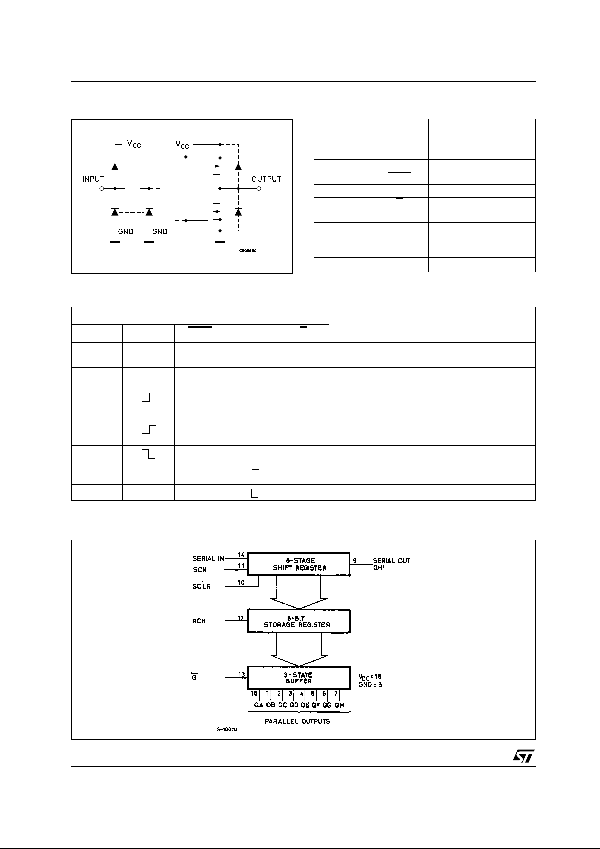
This device contains an 8-bit serial-in, parallel-out
shift register that feeds an 8-bit D -t y pe storage
register. The storage register has 8 3-STATE
outputs. Separate clocks a re provided for both t he
shift register and the storage register.
PIN CONNECTION AND IEC LOGIC SYMBOLS
The shift register has a direct-overriding clear,
serial input, and serial output (st andard) pins for
cascading. Both the shift register and storage
register use positive-edge t riggered clocks. If both
clocks are c onnec ted together, the shift r egister
state wi ll always be one clock pulse ahead of the
storage register.
All inputs a re equipped with protection circuits
against static discharge and transient excess
voltage.
1/16March 2004
M74HC595
INPUT AND OUTPUT EQUIVALENT CIRCUIT PIN DESCRIPTION
PIN N° SYMBOL NAME AND FUNCTION
1, 2, 3, 4, 5,
6, 7, 15
9 QH’ Serial Data Outputs
10 SCLR
11 SCK Shift Register Clock Input
13 G
14 SI Serial Data Input
12 RCK Storage Register Clock
8 GND Ground (0V)
16 V
TRUTH TABLE
QA to QH Data Outputs
CC
Shift Register Clear Input
Output Enable Input
Input
Positive Supply Voltage
INPUTS
SI SCK SCLR
X X X X H QA THRU QH OUTPUTS DISABLE
XXXXL QATHRUQHOUTPUTSENABLE
X X L X X SHIFT REGISTER IS CLEARED
LHXX
HHXX
X H X X STATE OF S.R. IS NOT CHANGED
XXX X
X X X X STORAGE REGISTER STATE IS NOT CHANGED
X: Don’t Care
RCK G
FIRST STAGE OF S.R. BECOMES "L" OTHER
STAGES STORE THE DATA OF PREVIOUS
FIRST STAGE OF S.R. BECOMES "H" OTHER
STAGES STORE THE DATA OF PREVIOUS
S.R. DATA IS STORED INTO STORAGE
OUTPUTS
STAGE, RESPECTIVELY
STAGE, RESPECTIVELY
REGISTER
LOGIC DIAGRAM
This logic diagram has not be used to estimate propagation delays
2/16

LOGIC DIAGRAM
This logic diagram has not be used to estimate propagation delays
M74HC595
TIMING CHART
3/16

M74HC595
ABSOLUTE MAXIMUM RATINGS
Symbol Parameter Value Unit
V
V
V
I
I
OK
I
I
or I
CC
P
T
T
Absolute Maximum Ratings are those values beyond which damage to the device may occur. Functional operation under these conditions is
not implied
(*) Power dissipation at 65°C. Derating from 65
RECOMMENDED OPERATING CONDITIONS
Symbol Parameter Value Unit
V
V
V
T
t
r,tf
Supply Voltage
CC
DC Input Voltage -0.5 to VCC+0.5
I
DC Output Voltage -0.5 to VCC+0.5
O
DC Input Diode Current
IK
DC Output Diode Current
DC Output Current
O
DC VCCor Ground Current
GND
-0.5 to +7 V
± 20 mA
± 20 mA
± 35 mA
± 70 mA
Power Dissipation DIP 750(*) mW
D
SOP 500(*) mW
TSSOP 450(*) mW
Storage Temperature
stg
Lead Temperature (10 sec)
L
-65 to +150 °C
300 °C
°Cto125°C: DIP Package -10mW/°C; SO Package -7mW/°C; TSSOP Package -6.1mW/°C.
Supply Voltage
CC
Input Voltage 0 to V
I
Output Voltage 0 to V
O
Operating Temperature
op
Input Rise and Fall Time VCC=2.0V
V
=4.5V
CC
=6.0V
V
CC
2to6 V
CC
CC
-55 to 125 °C
0 to 1000 ns
0 to 500 ns
0 to 400 ns
V
V
V
V
4/16

DC SPECIFICATIONS
Symbol Parameter
V
V
V
V
V
High Level Input
IH
Voltage
V
Low Level Input
IL
Voltage
High Level Output
OH
Voltage
(for QH’ outputs)
High Level Output
OH
Voltage
(for QA to QH
outputs)
Low Level Output
OL
Voltage
(for QH’ outputs)
Low Level Output
OL
Voltage
(for QA to QH
outputs)
Input Leakage
I
I
Current
I
High Impedance
OZ
Output Leakage
Current
Quiescent Supply
I
CC
Current
M74HC595
Test Condition Value
T
= 25°C
V
CC
(V)
A
Min. Typ. Max. Min. Max. Min. Max.
2.0 1.5 1.5 1.5
6.0 4.2 4.2 4.2
2.0 0.5 0.5 0.5
6.0 1.8 1.8 1.8
=-20 µA
2.0
4.5
6.0
4.5
6.0
2.0
4.5
6.0
4.5
6.0
2.0
4.5
6.0
4.5
6.0
2.0
4.5
6.0
4.5
6.0
V
6.0
6.0
6.0
I=VCC
V
VO=VCCor GND
V
I=VCC
I
O
=-20 µA
I
O
=-20 µA
I
O
=-4.0 mA
I
O
I
=-7.8 mA
O
=-20 µA
I
O
I
=-20 µA
O
=-20 µA
I
O
I
=-6.0 mA
O
=-7.8 mA
I
O
=20 µA
I
O
=20 µA
I
O
I
=20 µA
O
I
=4.0 mA
O
=7.8 mA
I
O
=20 µA
I
O
I
=20 µA
O
I
=20 µA
O
=6.0 mA
I
O
=7.8 mA
I
O
I=VIH
or GND
or V
or GND
1.9 2.0 1.9 1.9
4.4 4.5 4.4 4.4
5.9 6.0 5.9 5.9
4.18 4.31 4.13 4.10
5.68 5.8 5.63 5.60
1.9 2.0 1.9 1.9
4.4 4.5 4.4 4.4
5.9 6.0 5.9 5.9
4.18 4.31 4.13 4.10
5.68 5.8 5.63 5.60
0.0 0.1 0.1 0.1
0.0 0.1 0.1 0.1
0.0 0.1 0.1 0.1
0.17 0.26 0.33 0.40
0.18 0.26 0.33 0.40
0.0 0.1 0.1 0.1
0.0 0.1 0.1 0.1
0.0 0.1 0.1 0.1
0.17 0.26 0.33 0.40
0.18 0.26 0.33 0.40
IL
-40 to 85°C -55 to 125°C
± 0.1 ± 1 ± 1 µA
± 0.5 ± 5 ± 10 µA
44080µA
Unit
V4.5 3.15 3.15 3.15
V4.5 1.35 1.35 1.35
V
V
V
V
5/16

M74HC595
AC ELECTRICAL CHARACTERISTICS (CL= 50 pF, Input tr=tf=6ns)
Test Condition Value
T
Symbol Parameter
t
TLHtTHL
Output Transition
Time
(Qn)
t
TLHtTHL
Output Transition
Time
(QH’)
t
PLHtPHL
Propagation Delay
Time
(SCK - QH’)
t
PLHtPHL
t
PLHtPHL
Propagation Delay
Time
- QH’)
(SCLR
Propagation Delay
Time
(RCK - Qn)
t
PZLtPZH
High Impedance
Output Enable
Time
t
PLZtPHZ
High Impedance
Output Disable
Time
f
t
MAX
W(H)
Maximum Clock
Frequency
Minimum Pulse
Width
(SCK, RCK)
t
W(L)
t
s
Minimum Pulse
Width
)
(SCLR
Minimum Set-up
Time
(SI - CCK)
t
Minimum Set-up
s
Time
(SCK - RCK)
C
V
CC
(V)
L
(pF)
2.0
50
6.0 6 10 13 15
2.0
50
6.0 7 13 16 20
2.0
50
6.0 13 21 26 32
2.0
50
6.0 15 30 37 45
2.0
50
6.0 17 26 32 38
2.0
150
6.0 22 32 41 48
2.0
50
L
=1KΩ
R
6.0 13 23 29 35
2.0
R
150
=1KΩ
L
6.0 17 30 37 45
2.0
R
50
=1KΩ
L
6.0 14 26 32 38
2.0
50
6.0 35592824
2.0
150
6.0 31452520
2.0
50
6.0 6 13 16 19
2.0
50
6.0 6 13 16 19
2.0
50
6.0 4 9 11 13
2.0
50
6.0 6 13 16 19
= 25°C
A
Min. Typ. Max. Min. Max. Min. Max.
25 60 75 90
30 75 95 115
45 125 155 190
60 175 220 265
60 150 190 225
75 190 240 285
45 135 170 205
60 175 220 265
30 150 190 225
6.0 17 4.8 4
5.2 14 4.2 3.4
17 75 95 110
20 75 95 110
25 50 65 75
35 75 95 110
-40 to 85°C -55 to 125°C
Unit
ns4.5 7 12 15 18
ns4.5 8 15 19 23
ns4.5 15 25 31 38
ns4.5 18 35 44 53
ns4.5 20 30 38 45
ns4.5 25 38 48 57
ns4.5 15 27 34 41
ns4.5 20 35 44 53
ns4.5 15 30 38 45
MHz4.5 30502420
MHz4.5 26402117
ns4.5 6 15 19 22
ns4.5 6 15 19 22
ns4.5 5 10 13 15
ns4.5 8 15 19 22
6/16

M74HC595
Test Condition Value
= 25°C
Symbol Parameter
t
Minimum Set-up
s
Time
- RCK)
(SCRL
Minimum Hold
t
h
Time
C
V
CC
(V)
L
(pF)
2.0
50
6.0 7 17 21 25
2.0
50
T
A
Min. Typ. Max. Min. Max. Min. Max.
40 100 125 145
6.0 0 0 0
t
REM
Minimum Clear
Removal Time
2.0
15 50 65 75
50
6.0 3 9 11 13
CAPACITIVE CHARACTERISTICS
Test Condition Value
= 25°C
Symbol Parameter
V
CC
(V)
C
C
Input Capacitance
IN
Power Dissipation
PD
Capacitance (note
1)
1) CPDis defined as the value of the IC’s internal equivalent capacitance which is calculated from the operating current consumption without
load. (Refer to Test Circuit). Average operating current can be obtained by the following equation. I
T
A
Min. Typ. Max. Min. Max. Min. Max.
510 10 10pF
184 pF
-40 to 85°C -55 to 125°C
Unit
ns4.5 10 20 25 29
000
ns4.5 0 0 0
ns4.5 3 10 13 15
-40 to 85°C -55 to 125°C
CC(opr)=CPDxVCCxfIN+ICC
Unit
TEST CIRCUIT
TEST SWITCH
t
PLH,tPHL
t
PZL,tPLZ
t
PZH,tPHZ
CL= 50pF/150pF or equivalent (includes jig and probe capacitance)
=1KΩ or equivalent
R
1
R
T=ZOUT
of pulse generator (typically 50Ω)
Open
V
CC
GND
7/16

M74HC595
WAVEFORM 1: SCK TO QH’ PROPAGATION DELAY TIME S, SCK MINIMUM PULSE WIDTH
(f=1MHz; 50% duty cycle)
WAVEFORM 2: RCK TO Qn PROPAGATION DELAY TIMES (f=1MHz; 50% duty cycle)
WAVEFORM 3: SI TO SCK SETUP AND HO LD TIMES (f=1MHz; 50% duty cycle)
8/16

WAVEFORM 4: SCK TO RCK SETUP AND HOLD TIMES (f=1MHz; 50% duty cycle)
M74HC595
WAVEFORM 5: SCLR
MINIMUM PULSE W IDTH, MINIMUM REMOVAL TIME
(f=1MHz; 50% duty cycle)
9/16

M74HC595
WAVEFORM 6: OUTPUT ENABLE AND DISABLE TIMES (f=1MHz; 50% du ty cycle)
WAVEFORM 7: INPUT WAVEFORM (f=1MHz; 5 0% duty cycle)
10/16

M74HC595
Plastic DIP-16 (0.25) MECHANICAL DATA
mm. inch
DIM.
MIN. TYP MAX. MIN. TYP. MAX.
a1 0.51 0.020
B 0.77 1.65 0.030 0.065
b 0.5 0.020
b1 0.25 0.010
D 20 0.787
E 8.5 0.335
e 2.54 0.100
e3 17.78 0.700
F 7.1 0.280
I 5.1 0.201
L 3.3 0.130
Z 1.27 0.050
P001C
11/16

M74HC595
SO-16 MECHANICAL DATA
DIM.
A 1.75 0.068
a1 0.1 0.2 0.004 0.008
a2 1.65 0.064
b 0.35 0.46 0.013 0.018
b1 0.19 0.25 0.007 0.010
C 0.5 0.019
c1 45˚ (typ.)
D 9.8 10 0.385 0.393
E 5.8 6.2 0.228 0.244
e 1.27 0.050
e3 8.89 0.350
F 3.8 4.0 0.149 0.157
G 4.6 5.3 0.181 0.208
L 0.5 1.27 0.019 0.050
M 0.62 0.024
S8 ˚ (max.)
MIN. TYP MAX. MIN. TYP. MAX.
mm. inch
12/16
PO13H

M74HC595
TSSOP16 MECHANICAL DATA
mm. inch
DIM.
MIN. TYP MAX. MIN. TYP. MAX.
A 1.2 0.047
A1 0.05 0.15 0.002 0.004 0.006
A2 0.8 1 1.05 0.031 0.039 0.041
b 0.19 0.30 0.007 0.012
c 0.09 0.20 0.004 0.0079
D 4.9 5 5.1 0.193 0.197 0.201
E 6.2 6.4 6.6 0.244 0.252 0.260
E1 4.3 4.4 4.48 0.169 0.173 0.176
e 0.65 BSC 0.0256 BSC
K0˚ 8˚ 0˚ 8˚
L 0.45 0.60 0.75 0.018 0.024 0.030
A2
A
A1
b
e
c
K
L
E
D
E1
PIN 1 IDENTIFICATION
1
0080338D
13/16

M74HC595
Tape & Reel SO-16 MECHANICAL DATA
mm. inch
DIM.
MIN. TYP MAX. MIN. TYP. MAX.
A 330 12.992
C 12.8 13.2 0.504 0.519
D 20.2 0.795
N 60 2.362
T 22.4 0.882
Ao 6.45 6.65 0.254 0.262
Bo 10.3 10.5 0.406 0.414
Ko 2.1 2.3 0.082 0.090
Po 3.9 4.1 0.153 0.161
P 7.9 8.1 0.311 0.319
14/16

M74HC595
Tape & Reel TSSOP16 MECHANICAL DATA
mm. inch
DIM.
MIN. TYP MAX. MIN. TYP. MAX.
A 330 12.992
C 12.8 13.2 0.504 0.519
D 20.2 0.795
N 60 2.362
T 22.4 0.882
Ao 6.7 6.9 0.264 0.272
Bo 5.3 5.5 0.209 0.217
Ko 1.6 1.8 0.063 0.071
Po 3.9 4.1 0.153 0.161
P 7.9 8.1 0.311 0.319
15/16

M74HC595
Information furnished is believed to be accurate and reliable. However, STMicroelectronics assumes no responsibility for the
consequences of use of such inform ation nor fo r an y infring ement of p atents or o ther rights of third p arties which may r esult f rom
its use. No license is granted by implication or otherwise under any patent or patent rights of STMicroelectronics. Specifications
mentioned in this publication are subject to change without notice. This publication supersedes and replaces all information
previously supplied. STMicroelectronics products are not authorized for use as critical components in life support devices or
systems without express written approval of STMicroelectronics.
Australia - Belgium - Brazil - Canada - China - Czech Republic - Finland - France - Germany - Hong Kong - India - Israel - Italy - Japan -
Malaysia - Malta - Morocco - Singapore - Spain - Sweden - Switzerland - United Kingdom - United States.
The ST logo is a registered trademark of STMicroelectronics
All other names are the property of their respective owners
© 2004 STMicroelectronics - All Rights Reserved
STMicroelectronics GROUP OF COMPANIES
http://www.st.com
16/16
 Loading...