

M74HC590
8 BINARY COUNTER REGISTER
WITH 3 STATE OUTPUT
■ HIGH SPEED:
f
= 61 MHz (TYP.) at VCC = 6V
MAX
■ LOW POWER DISSIPATION:
I
= 4µA(MAX.) at TA=25°C
CC
■ HIGH NOISE IMMUNITY:
V
= V
NIH
■ SYMMETRICAL OUTPUT IMPEDANCE:
|I
| = IOL = 6mA (MIN) for QA ~ QH OUTPUT
OH
|I
| = IOL = 4mA (MIN) for RCO OUTPUT
OH
■ BALANCED PROPAGATION DELAYS:
t
≅ t
PLH
■ WIDE OPERATING VOLTAGE RANGE:
V
(OPR) = 2V to 6V
CC
■ PIN AND FUNCTION COMPATIBLE WITH
= 28 % VCC (MIN.)
NIL
PHL
74 SERIES 590
DESCRIPTION
The M74HC590 is a n high speed CMOS 8-BIT
BINARY COUNTER REGISTER (3 STATE)
fabricated with silicon gate C
2
MOS technology.
This device contains an 8-bit bin ary counter that
feeds an 8-bit storage register. The storage
register has parallel outputs. Separate clocks are
provided for both the bin ary counter and storage
register. The binary counter features a direct clear
input CCLR
and a count enable input CCKEN. For
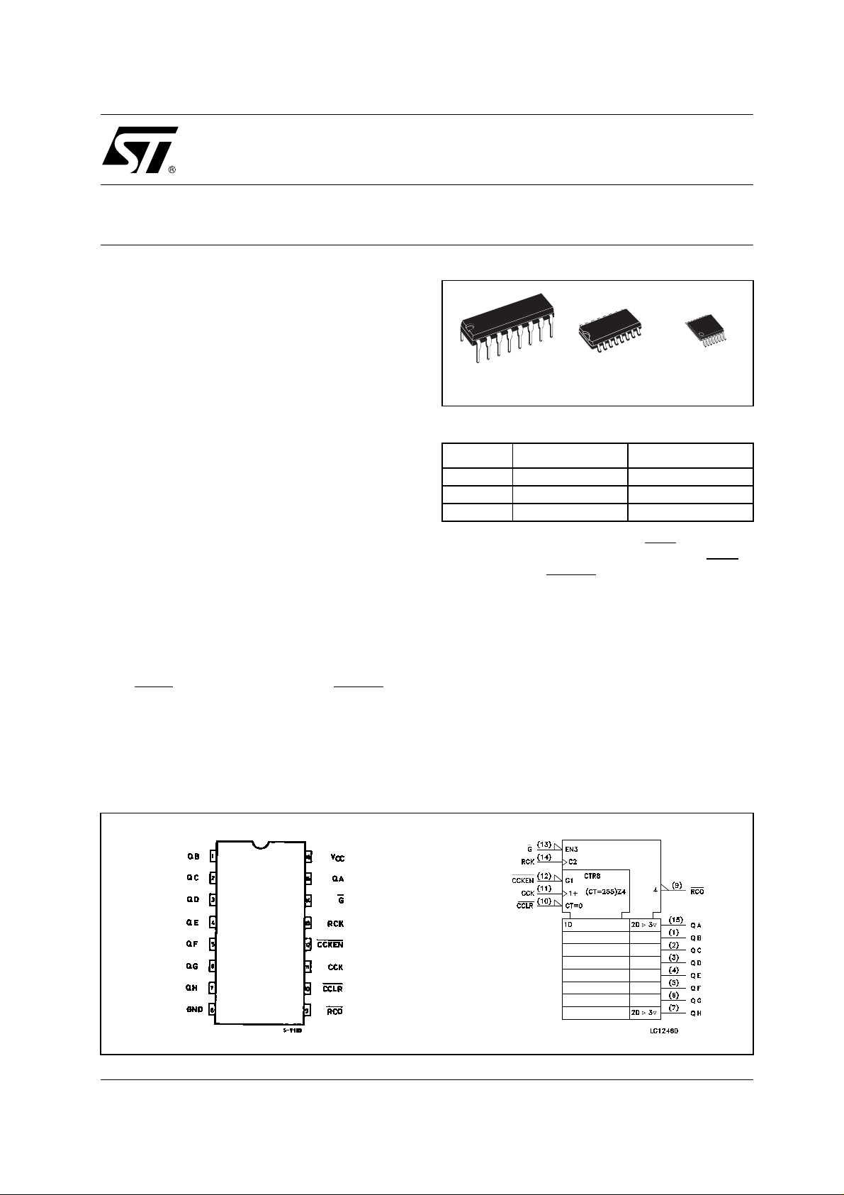
TSSOPDIP SOP
ORDER CODES
PACKAGE TUBE T & R
DIP M74HC590B1R
SOP M74HC590M1R M74HC590RM13TR
TSSOP M74HC590TTR
cascading, a ripple carry output RCO
Expansion is easily accomplished by tying RCO
the first stage to CCKEN
of the second stage, etc.
is provided.
of
Both the counter and register clocks are positive
edge triggered. If the user wishes to connect bot h
clocks together, the counter state will always be
one count ahead of the register. Internal circuitry
prevents clocking from the clock enable. All inputs
are equipped with protection circuits against static
discharge and transient excess voltage.
PIN CONNECTION AND IEC LOGIC SYMBOLS
1/15August 2001

M74HC590
INPUT AND OUTPUT EQUIVALENT CIRCUIT PIN DESCRIPTION
PIN No SYMBOL NAME AND FUNCTION
1, 2, 3, 4, 5,
6, 7, 15
11 CCK Counter Clock Input
12 CCKEN
13 RCK Register Clock Input
9RCO
14 G Output Enable Input
10 CCLR
8 GND Ground (0V)
16 V
TRUTH TABLE
QA to QH Outputs
CC
Counter Clock Enable
Input
Ripple Carry Output
Counter Clear Input
Positive Supply Voltage
INPUTS
G
H X X X X Q OUTPUTS DISABLE
L X X X X Q OUTPUTS ENABLE
X X X X COUNTER DATA IS STORED INTO REGISTER
X X X X REGISTER STAGE IS NOT CHANGED
X X L X X COUNTER CLEAR
X X H L ADVANCE ONE COUNT
X X H L NO COUNT
X X H H X NO COUNT
X: Don’t Care
RCO
= QA’·QB’·QC’· QD’ ·QE’·Q F’·Q G’·Q H’ (QA’ to QH’ : INTERNAL OUTPUTS OF THE COUNTER)
RCK CCLR CCKEN CCK
OUTPUT
LOGIC DIAGRAM
2/15
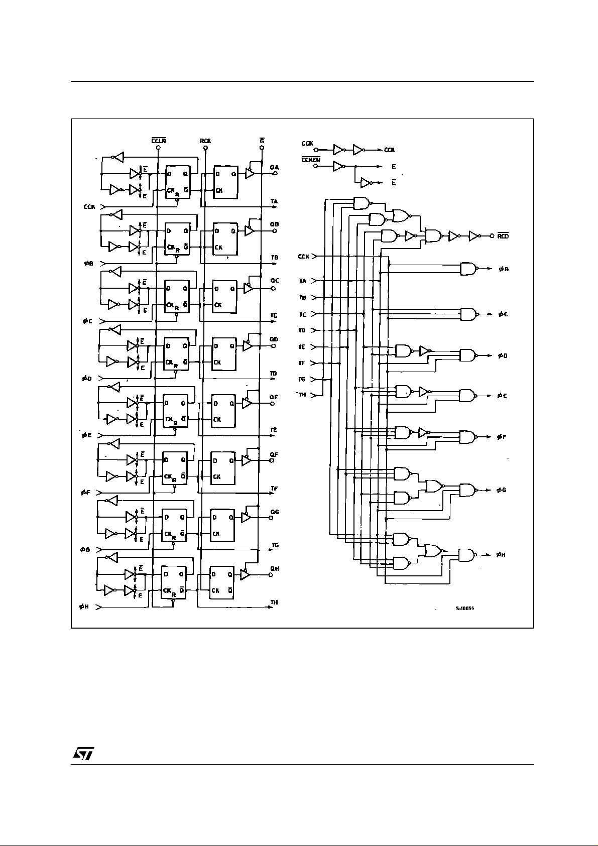
LOGIC DIAGRAM
M74HC590
This log i c diagram has not be used to esti m ate propagation delays
3/15
M74HC590
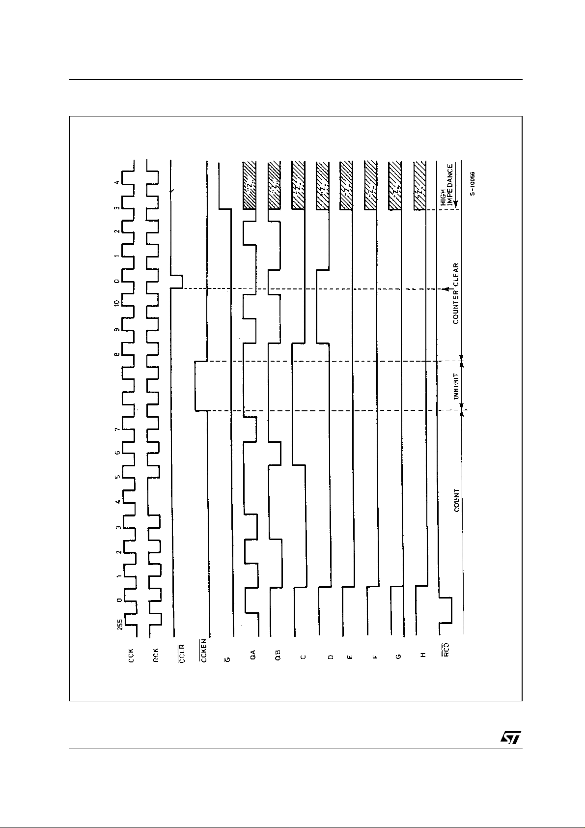
TIMING CHART
4/15
M74HC590
ABSOLUTE MAXIMUM RATINGS
Symbol Parameter Value Unit
V
V
V
I
I
OK
I
I
or I
CC
P
T
T
Absolute Maximum Ratings are those values beyond which damage to the device may occur. Functional operation under these conditions is
not implied
(*) 500mW at 65
RECOMMENDED OPERATING CONDITIONS
Symbol Parameter Value Unit
V
V
V
T
t
r
Supply Voltage
CC
DC Input Voltage -0.5 to VCC + 0.5
I
DC Output Voltage -0.5 to VCC + 0.5
O
DC Input Diode Current
IK
DC Output Diode Current
DC Output Source Sink Current per Output PIN (RCO)
O
(QA - QH)
DC VCC or Ground Current
GND
Power Dissipation
D
Storage Temperature
stg
Lead Temperature (10 sec)
L
°C; derate to 300mW by 10mW/°C from 65°C to 85°C
Supply Voltage
CC
Input Voltage 0 to V
I
Output Voltage 0 to V
O
Operating Temperature
op
Input Rise and Fall Time VCC = 2.0V
, t
f
V
V
CC
CC
= 4.5V
= 6.0V
-0.5 to +7 V
± 20 mA
± 20 mA
± 25
± 35
mA
± 70 mA
500(*) mW
-65 to +150 °C
300 °C
2 to 6 V
CC
CC
-55 to 125 °C
0 to 1000 ns
0 to 500 ns
0 to 400 ns
V
V
V
V
5/15
 Loading...