

M74HC4543
BCD T O 7 SEGM ENT LATCH/D ECODER/LCD DRIVER
■ HIGH SPEED:
t
= 14ns (TYP.) at VCC = 6V
PD
■ LOW POWER DISSIPATION:
I
= 4µA(MAX.) at TA=25°C
CC
■ HIGH NOISE IMMUNITY:
V
= V
NIH
■ SYMMETRICAL OUTPUT IMPEDANCE:
|I
| = IOL = 4mA (MIN)
OH
■ BALANCED PROPAGATION DELAYS:
t
≅ t
PLH
■ WIDE OPERATING VOLTAGE RANGE:
V
(OPR) = 2V to 6V
CC
■ PIN AND FUNCTION COMPATIBLE WITH
= 28 % VCC (MIN.)
NIL
PHL
74 SERIES 4543
DESCRIPTION
The M74HC4543 is an high speed CMOS
BCD-TO-7 SEGMENT DECODER WITH LCD
DRIVER fabricated with silicon gate C
2
MOS
technology.
This device consists of BCD-TO-7 segment
decoder with a BCD input latch and a 7-s egment
driver for a liquid crystal display (LCD). When any
illegal BCD input signal is applied or input BI is
held high, the display is blanked. When driving
TSSOPDIP SOP
ORDER CODES
PACKAGE TUBE T & R
DIP M74HC4543B1R
SOP M74HC4543M1R M74HC4543RM13TR
TSSOP M74HC4543TTR
LCDs, a commo n square wave signal should be
applied not only to the PH input of this device but
also to the electrically common backplan e of the
display. For other types of readouts, such as
light-emitting diode (LED), some additional
drivers, such as a transistor array is required. All
inputs are equipped with protection circuits
against static discharge and transient excess
voltage.
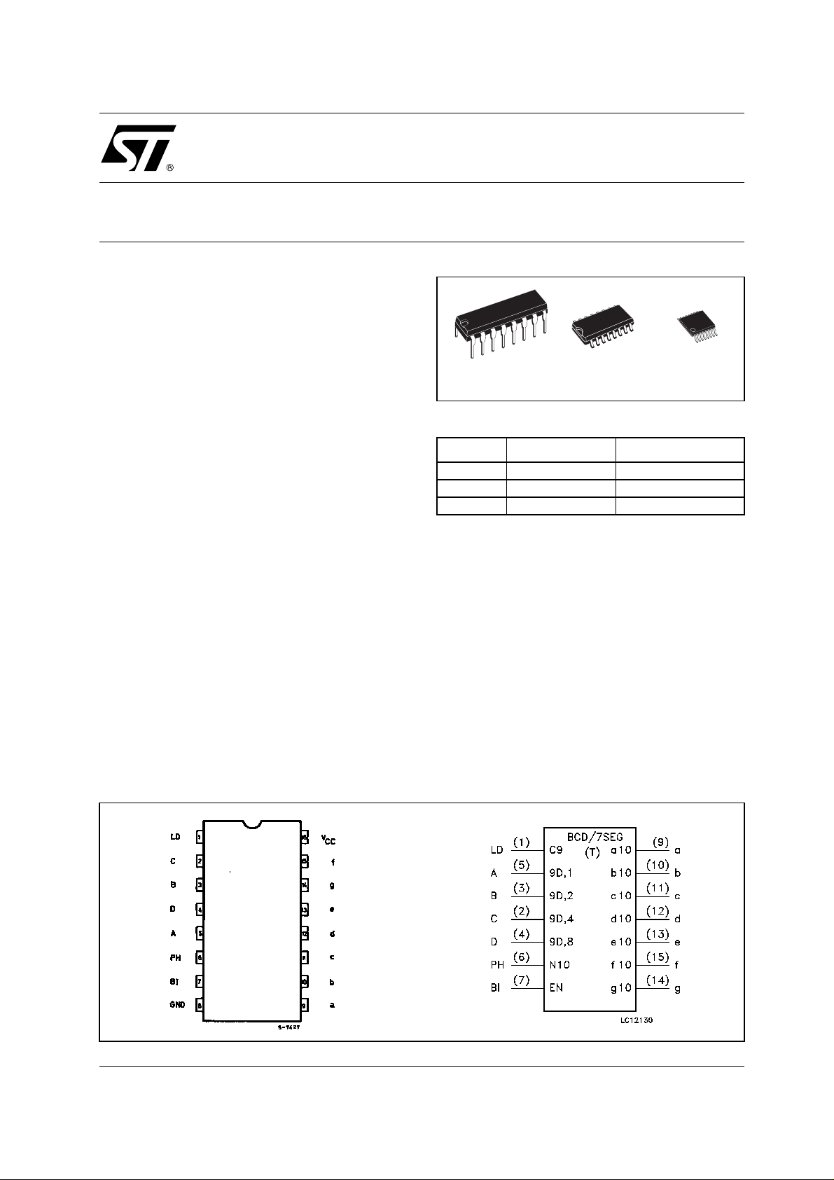
PIN CONNECTION AND IEC LOGIC SYMBOLS
1/10July 2001
M74HC4543
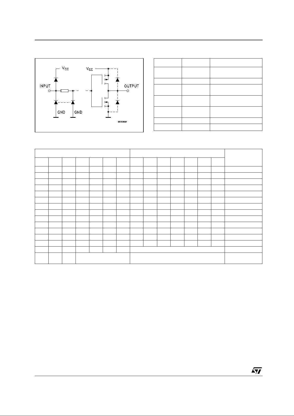
INPUT AND OUTPUT EQUIVALENT CIRCUIT PIN DESCRIPTION
PIN No SYMBOL NAME AND FUNCTION
1 LD Latch Disable Input
5, 3, 2, 4 A to D Address (Data) Inputs
6 PH Phase Input (Active
7 BI Blanking Input (Active
9, 10, 11, 12,
13, 15, 14
8 GND Ground (0V)
16 V
TRUTH TABLE
a to g Segment Outputs
CC
(Active HIGH)
HIGH)
HIGH)
Positive Supply Voltage
INPUT OUTPUT
DISPLAY MODE
LD BI PH D C B A a b c d e f g
X H L X X X X L L L L L L L BLANK
HLLLLLLHHHHHHL 0
HLLLLLHLHHLLLL 1
HLLLLHLHHLHHLH 2
HLLL LHHHHHHL LH 3
HLLLHLLLHHLLHH 4
HLLLHLHHLHHLHH 5
HLLLHHLHLHHHHH 6
HLLLHHHHHHLLLL 7
HLLHLLLHHHHHHH 8
HLLHLLHHHHHLHH 9
H L L H L H X L L L L L L L BLANK
H L L H H X X L L L L L L L BLANK
L L L X X X X ##### #####
↑↑H ↑ INVERSE OF ABOVE OUTPUT LEVEL
X : Don’t Care
↑ : Same as above com bi nations
### : Depends upon the BC D code previously applied when LD =’H’
DISPLAY AS
ABOVE
2/10
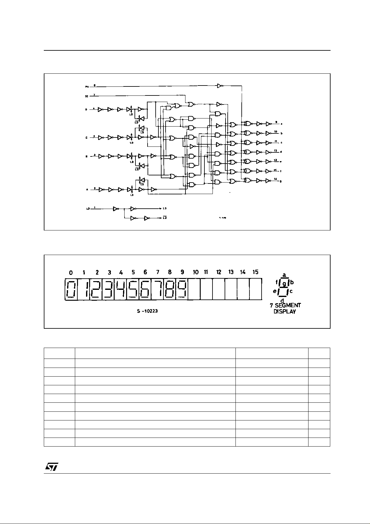
LOGIC DIAGRAM
M74HC4543
This log i c diagram has not be used to est i m at e propagation delays
DISPLAY MODE
ABSOLUTE MAXIMUM RATINGS
Symbol Parameter Value Unit
V
V
V
I
I
OK
I
I
or I
CC
P
T
T
Absolute Maximum Ratings are those values beyond which damage to the device may occur. Functional operation under these conditions is
not implied
(*) 500mW at 65
Supply Voltage
CC
DC Input Voltage -0.5 to VCC + 0.5
I
DC Output Voltage -0.5 to VCC + 0.5
O
DC Input Diode Current
IK
DC Output Diode Current
DC Output Current
O
DC VCC or Ground Current
GND
Power Dissipation
D
Storage Temperature
stg
Lead Temperature (10 sec)
L
°C; derate to 300mW by 10mW/°C from 65°C to 85°C
-0.5 to +7 V
V
V
± 20 mA
± 20 mA
± 25 mA
± 50 mA
500(*) mW
-65 to +150 °C
300 °C
3/10
 Loading...