


Features
■ High speed:
t
= 25 ns (typ.) at VCC = 6 V
PD
■ Low power dissipation
standby state:
I
= 4 μA (max.) at TA=25°C
CC
active state:
I
= 200 μA (max.) at VCC=6V
CC
■ High noise immunity:
V
= V
NIH
■ Symmetrical output impedance:
|I
| = IOL = 4 mA (min.)
OH
■ Balanced propagation delays:
t
≅ t
PLH
■ Wide operating voltage range:
V
(opr) = 2 to 6 V
CC
■ Wide output pulse width range:
t
WOUT
■ Pin and function compatible with
74 series 4538
Table 1. Device summary
NIL
PHL
= 28 % V
CC
(min.)
= 120 ns ~ 60 s over at VCC = 4.5 V
M74HC4538
Dual retriggerable monostable multivibrator
SO-16
DIP-16
TSSOP16
Description
The M74HC4538 is a high speed CMOS monostable
multivibrator fabricated with silicon gate C2MOS
technology.
Each multivibrator features both a negative A, and a
positive B, edge triggered input, either of which can be
used as an inhibit input. Also included is a clear input
that when taken low resets the one shot. The
monostable multivibrators are retriggerable. That is,
they may be triggered repeatedly while their outputs are
generating a pulse and the pulse will be extended.
Pulse width stability over a wide range of temperature
and supply is achieved using linear CMOS techniques.
The output pulse equation is simply: PW = 0.7 (R)(C)
where PW is in seconds, R in Omhs and C is in Farads.
All the inputs are equipped with protection circuits
against static discharge and transient excess voltage.
Order code Package Packaging
M74HC4538B1R DIP-16 Tube
M74HC4538RM13TR SO-16 Tape and reel
M74HC4538TTR TSSOP16 Tape and reel
May 2008 Rev 2 1/18
www.st.com
18

Pin connection and IEC logic symbols M74HC4538
1 Pin connection and IEC logic symbols
Figure 1. Pin connections and IEC logic symbols
V
16
CC
15
2T1
14
2T2
13
2CD
Inputs
12
2A
11
2B
10
9
Outputs
Q2
Q2
Inputs
Outputs
1T1
1T2
1CD
1A
1B
Q1
Q1
GND
1
2
3
4
5
6
7
8
Table 2. Pin description
Pin number Symbol Name and function
1, 15 1T1, 2T1 External capacitor connections
2, 14 1T2, 2T2 External resistor, capacitor connections
3, 13 1CD,
4, 12 1A, 2A Trigger inputs (low to high, edge-triggered)
5, 11 1B, 2B Trigger inputs (high to low, edge-triggered)
6, 10 Q1, Q2 Pulse outputs
2CD Direct reset inputs (active low)
7, 9 Q1, Q2 Complementary pulse outputs
8 GND Ground (0 V)
16 V
CC
Positive supply voltage
2/18

M74HC4538 Pin connection and IEC logic symbols
Figure 2. Input and output equivalent circuit
GND
V
CC
Output
Input
Table 3. Truth table
V
CC
GND
Inputs Outputs
AB
CD QQ
H H Output enable
X L H L H Inhibit
H X H L H Inhibit
L H Output enable
X X L L H Inhibit
Note
Figure 3. System diagram
3/18
Pin connection and IEC logic symbols M74HC4538
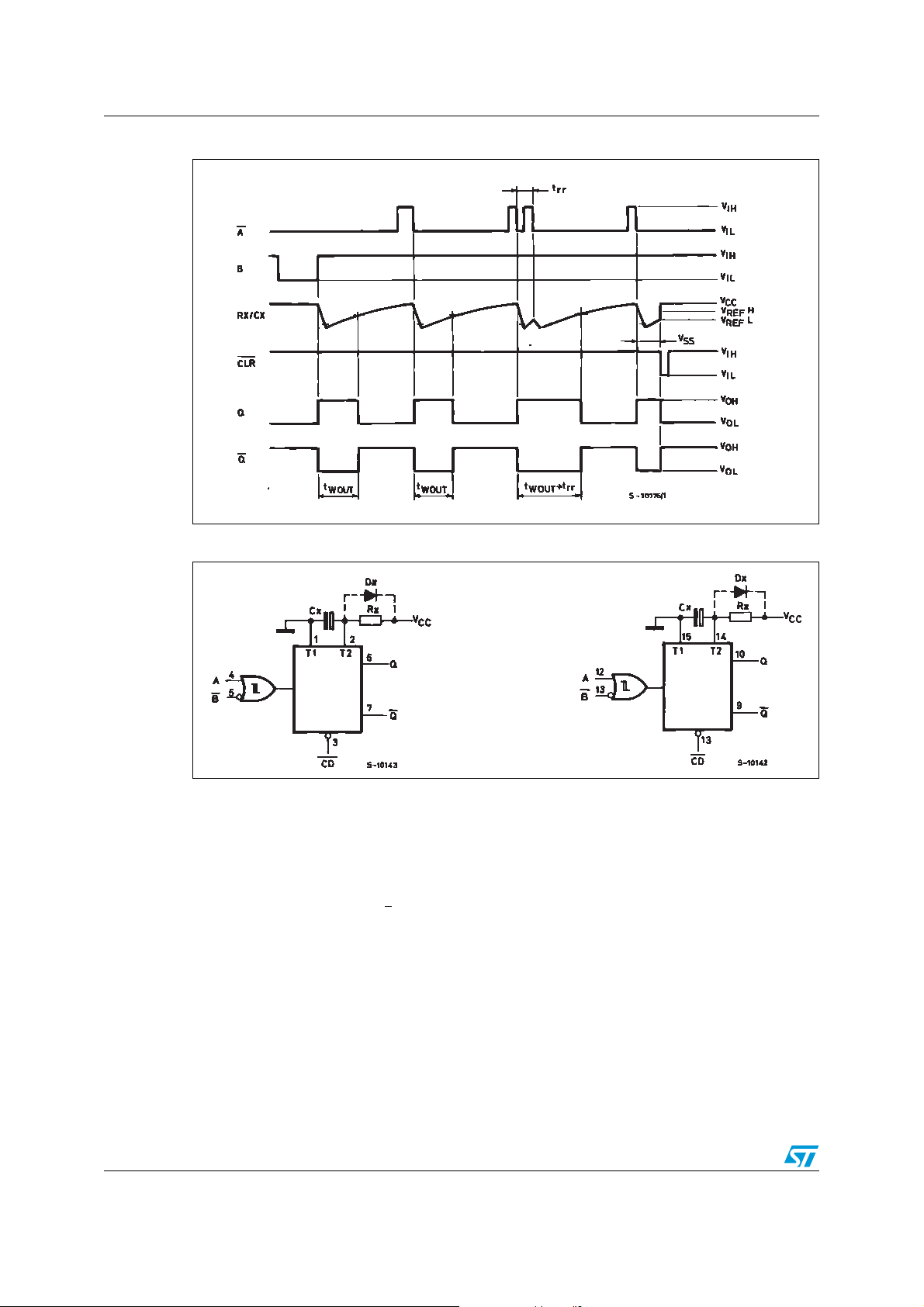
Figure 4. Timing chart
Figure 5. Block diagram
1. Cx, Rx, Dx are external components.
2. Dx is a clamping diode.
The external capacitor is charged to V
turned off Cx is discharged mainly through an internal parasitic diode (see figures). If Cx is sufficiently large
and V
up. If the voltage supply filter capacitor is large enough and V
automatically limited and damage to the IC is avoided. The maximum forward current of the parasitic diode
is approximately 20 mA. In cases where Cx is large the time taken for the supply voltage to fall to 0.4 V
can be calculated as follows: t
In cases where t
current.
decreases rapidly, there will be some possibility of damaging the IC with a surge current or latch-
CC
> (VCC - 0.7) x Cx/20 mA.
is too short an external clamping diode is required to protect the IC from the surge
f
f
in the standby state, i.e. no trigger. When the supply voltage is
CC
decreases slowly, the surge current is
CC
CC
4/18

M74HC4538 Functional description
2 Functional description
Standby state
The external capacitor Cx, is fully charged to VCC in the standby state. Hence, before
triggering, transistor Qp and Qn (connected to th e Rx/Cx node) are both turned-off . The two
comparators that control the timing and the two reference voltage sources stop operating.
The total supply current is therefore only leakage current.
Trigger operation
Triggering occurs when:
– A is low and B has a falling edge
– B is high and A has a rising edge
After the multivibrator has been retriggered, t he comparator C1 and C2 start operating and
Qn is turned on. Cx then discharges through Qn. The voltage at the node Rx/Cx external
falls.
When it reaches V
the output of comparator C1 becomes low. This in turn resets the
REFL
flip-flop and Qn is turned off.
At this point C1 stops functioning but C2 continues to operate.
The voltage at R/C external begins to rise with a time constant set by the external
components Rx and Cx.
Triggering the multivibrator causes Q to go high after internal delay due to the flip-flop and
the gate. Q remains high unt il the voltage at R/C e xte rnal rises again to V
. At this point
REFH
C2 output goes low and G goes low. C2 stops operating. That means that after triggering
when the voltage R/C external returns to V
the multivibrator has returned to its
REFH
monostable state . In the case where Rx · Cx are la rge enough and the d ischarge time of the
capacitor and the delay time in the IC can be ignored, the width of the output pulse t
w(out)
is
as follows:
)OUT(W
Rx•Cx72.0=t
Re-triggered operation
When a second triggered pulse follows the first, its effect will depend on the state of the
multivibrator. If the capacitor Cx is being charged, the v oltag e level of Rx/Cx e xternal falls to
V
again and Q remains high i.e. the retrigger pulse arrives in a time shorter than the
REFL
period Rx · Cx seconds, the capacitor charging time constant. If the second trigger pulse is
very close to the initial trigger pulse it is ineffective; i.e. the second trigger m ust arriv e in t he
capacitor discharge cycle to be ineffective; hence the minimu m time for a second trigger to
be effective, t
(min.) depends on VCC and Cx.
rr
Reset operation
CD is normally high. If CD is low, the trigger is not effective because Q output goes lo w an d
trigger control flip-flop is reset. Also transistor Op is turned on and Cx is charged quickly to
V
. Then, if CD input goes low the IC becomes waiting state both in operating and non
CC
operating state.
5/18

Maximum rating M74HC4538
3 Maximum rating
Stressing the device above the rating listed in the “Absolute maximum ratings” table may
cause permanent damage to the device. These are stre ss r a tings only, and operation of the
device at these or any other conditions above those indicated in the operating sections of
this specification is not implied. Exposure to absolute maximum rating conditions for
extended periods may affect device reliability. Refer also to the STMicroelectronics SURE
Program and other relevant quality documents.
Table 4. Absolute maximum ratings
Symbol Parameter Value Unit
V
V
I
I
CC
I
GND
P
T
1. 500mW at 65 ° C; derate to 300 mW by 10 mW/ ° C from 65° C to 85° C
Supply voltage -0.5 to +7 V
CC
DC input voltage -0.5 to VCC + 0.5 V
V
I
DC output voltage -0.5 to VCC + 0.5 V
O
I
DC input diode current ± 20 mA
IK
DC output diode current ± 20 mA
OK
I
DC output current ± 25 mA
O
or
DC VCC or ground current ± 50 mA
Power dissipation 500
D
Storage temperature -65 to +15 0 °C
stg
Lead temperature (10 sec) 300 °C
T
L
3.1 Recommended operating conditions
Table 5. Recommended operating conditions
Symbol Parameter Value Unit
V
V
T
t
Cx External capacitor No limitation pF
Supply voltage 2 to 6 V
CC
Input voltage 0 to V
V
I
Output voltage 0 to V
O
Operating temperature -55 to 125 °C
op
= 2.0 V 0 to 1000 ns
V
CC
, tfInput rise and fall time (CD only)
r
V
= 4.5 V 0 to 500 ns
CC
= 6.0 V 0 to 400 ns
V
CC
(1)
CC
CC
mW
V
V
Rx External resistor
6/18
VCC ≤ 3.0 V 5 K to 1 M
≥ 3.0 V 1 K to 1 M
V
CC
Ω

M74HC4538 Electrical characteristics
4 Electrical characteristics
Table 6. DC specifications
Test condition Value
Symbol Parameter
V
V
V
V
I
High level input
IH
voltage
Low level input
IL
voltage
High level output
OH
voltage
Low level output
OL
voltage
Input leakage
I
I
current
Input leakage
I
I
current
Quiescent supply
CC
current
= 25°C -40 to 85°C
T
V
CC
A
-55 to
125°C
(V)
Min Typ Max Min Max Min Max
2.0 1.5 1.5 1.5
6.0 4.2 4.2 4.2
2.0 0.5 0.5 0.5
6.0 1.8 1.8 1.8
2.0 I
4.5 I
6.0 I
4.5 I
6.0 I
2.0 I
4.5 I
6.0 I
4.5 I
6.0 I
6.0 V
6.0
6.0 V
=-20 μA 1.9 2.0 1.9 1.9
O
=-20 μA 4.4 4.5 4.4 4.4
O
=-20 μA 5.9 6.0 5.9 5.9
O
= -4.0 mA 4.18 4.31 4.13 4.10
O
= -5.2 mA 5.68 5.8 5.63 5.60
O
= 20 μA 0.0 0.1 0.1 0.1
O
= 20 μA 0.0 0.1 0.1 0.1
O
= 20 μA 0.0 0.1 0.1 0.1
O
= 4.0 mA 0.17 0.26 0.33 0.40
O
= 5.2 mA 0.18 0.26 0.33 0.40
O
= VCC or GND ± 0.1 ± 1 ± 1 μA
I
= VCC or GND
V
I
Rext/Cext
= VCC or GND 4 40 80 μA
I
± 0.1 ± 1 ± 1 μA
Unit
V4.5 3.15 3.15 3.15
V4.5 1.35 1.35 1.35
V
V
2.0
I
Quiescent supply
CC
current
4.5 0.2 0.3 0.4 0.6 mA
6.0 0.3 0.6 0.8 1.0 mA
= VCC or GND
V
I
Pin 2 or 14
VIN = VCC/2
40 120 160 200 μA
7/18

Electrical characteristics M74HC4538
Table 7. AC electric al characteristics (C
Test co ndition Valu e
= 50 pF, Input tr = tf = 6 ns)
L
Symbol Parameter
t
TLH tTHL
Output transition
time
Propagation
t
PLH tPHL
delay time
- Q, Q)
(A, B
Propagation
t
PLH tPHL
t
WOUT
delay time
- Q, Q)
(CD
Output pulse
width
V
CC
TA = 25°C -40 to 85°C
-55 to
125°C
Unit
(V)
Min Typ Max Min Max Min Max
2.0 30 75 95 110
ns4.5 8 15 19 22
6.0 7 13 16 19
2.0 120 250 315 375
ns4.5 30506375
6.0 25435464
2.0 100 195 245 295
ns4.5 25394959
6.0 20334250
2.0
Cx=0
6.0 Rx = 1 K
2.0
Rx = 5 KΩ 540 1200 1500 1800
Ω 180 250 320 375
Ω 150 200 260 320
70 83 96 70 96 70 96
Cx = 0.01 μF
Rx = 10 K
Ω
ns4.5 Rx = 1 K
μs4.5 69778569856985
6.0 69778569856985
Δt
WOUT
t
W(H) tW(L)
t
W(L)
t
REM
Output pulse
width error
between circuits
in same package
Minimum pulse
width
)
(A,B
Minimum pulse
width
)
(CD
Minimum clear
removal time
2.0
0.67 0.75 0.83 0.67 0.83 0.67 0.9
Cx = 0.1 μF
Rx = 10 K
Ω
6.0 0.670.730.770.670.770.67 0.8
±1 %
2.0 30 75 95 110
6.0 7 13 16 19
2.0 30 75 95 110
6.0 7 13 16 19
2.0 0 15 15 20
6.0 0 5 5
ms4.5 0.670.730.770.670.770.67 0.8
ns4.5 8 15 19 22
ns4.5 8 15 19 22
ns4.5 0 5 5 7
8/18

M74HC4538 Electrical characteristics
Table 7. AC electric al characteristics (C
= 50 pF, Input tr = tf = 6 ns) (continued)
L
Test co ndition Valu e
Symbol Parameter
V
CC
TA = 25°C -40 to 85°C
-55 to
125°C
(V)
Min Typ Max Min Max Min Max
2.0
380
Cx = 0.1 μF
Rx = 1K
6.0 72
2.0
rr
Minimum
retrigger time
t
Ω
6
Cx = 0.01μF
Rx = 1K
Ω
6.0 1.2
Table 8. Capacitive characteristics
Test condition Value
Symbol Parameter
V
CC
(V)
C
C
1. CPD is defined as the value of the IC’s internal equivalent capacitance which is calculated from the operating current
consumption without load. (Refer to Test Circuit). Average operating current can be obtained by the following equation.
I
CC(opr)
Input capacitance 5.0 5 10 10 10 pF
IN
Power dissipation
PD
capacitance
= CPD x VCC x fIN + ICC’ Duty/100 + Ic/2(per monostable) (Icc’ : Active Supply current) (Duty : %)
(1)
5.0 70 pF
TA = 25°C -40 to 85°C -55 to 125°C
Min Typ Max Min Max Min Max
Unit
ns4.5 92
μs4.5 1.4
Unit
9/18

Electrical characteristics M74HC4538
Figure 6. Test circuit
Figure 7. Waveform: propagation delay times (f = 1 MHz; 50% duty cycle)
10/18

M74HC4538 Package mechanical data
5 Package mechanical data
In order to meet environmental requirements, ST offers these devices in ECOPACK®
packages. These packages have a Lead-free second level interconnect. The category of
second level inte rconnect is marked on the package and on the inner box label, in
compliance with JEDEC Standard JESD97. The maximum ratings related to soldering
conditions are also marked on the inner box label. ECOPACK is an ST trademark.
ECOPACK specifications are available at: www.st.com.
11/18

Package mechanical data M74HC4538
Plastic DIP-16 (0.25) MECHANICAL DATA
DIM.
MIN. TYP MAX. MIN. TYP. MAX.
a1 0.51 0.020
B 0.77 1.65 0.030 0.065
b 0.5
b1 0.25 0.010
D 20 0.787
E 8.5 0.335
e 2.54 0.100
e3 17.78 0.700
F 7.1 0.
I 5.1 0.201
L 3.3 0.130
Z 1.27 0.050
mm. inch
0.020
280
12/18
P001C

M74HC4538 Package mechanical data
SO-16 MECHANICAL DATA
DIM.
A1.750.068
a1 0.1 0.25 0.004 0.010
a2 1.64 0.063
b 0.35 0.46 0.013 0.018
b1 0.19 0.25 0.007 0.010
C 0.5 0.019
c1 45° (typ.)
D9.8 10 0.3850.393
E5.8 6.2 0.228 0.244
e 1.27 0.050
e38.890.350
F 3.8 4.0 0.149 0.157
G4.6 5.3 0.1810.208
L 0.5 1.27 0.019 0.050
M 0.62 0.024
S8° (max.)
MIN. TYP MAX. MIN. TYP. MAX.
mm. inch
0016020D
13/18

Package mechanical data M74HC4538
TSSOP16 MECHANICAL DATA
DIM.
A 1.2 0.047
A1 0.05 0.15 0.002 0.004 0.006
A2
b 0.19 0.30 0.007 0.012
c 0.09 0.20 0.004 0.0079
D 4.9 5 5.1 0.193 0.197 0.201
E 6.2 6.4 6.6 0.244 0.252 0.260
E1 4.3 4.4 4.48 0.169 0.173 0.176
e 0.65 BSC 0.0256 BSC
K0
L 0.45 0.60 0.75 0.018 0.024 0.030
MIN. TYP MAX.
0.8 1 1.05 0.031 0.039 0.041
°8°0°8°
A2
A
A1
mm. inch
b
e
c
MIN. TYP. MAX.
K
L
E
D
PIN 1 IDENTIFICATION
1
14/18
E1
0080338D

M74HC4538 Package mechanical data
Tape & Reel SO-16 MECHANICAL DATA
DIM.
MIN. TYP MAX. MIN. TYP. MAX.
A 330
C 12.8 13.2 0.504 0.519
D 20.2 0.795
N 60 2.362
T 22.4 0.882
Ao 6.45 6.65 0.254 0.262
Bo 10.3
Ko 2.1 2.3 0.082 0.090
Po 3.9 4.1 0.153 0.161
P 7.9 8.1 0.311 0.319
mm. inch
12.992
10.5 0.406 0.414
15/18

Package mechanical data M74HC4538
Tape & Reel TSSOP16 MECHANICAL DATA
DIM.
A 330
C 12.8 13.2 0.504 0.519
D 20.2 0.795
N 60 2.362
T 22.4 0.882
Ao 6.7 6.9 0.264 0.272
Bo 5.
Ko 1.6 1.8 0.063 0.071
Po 3.9 4.1 0.153 0.161
P 7.9 8.1 0.311 0.319
MIN. TYP MAX. MIN. TYP. MAX.
3 5.5 0.209 0.217
mm. inch
12.992
16/18

M74HC4538 Revision history
6 Revision history
Table 9. Document revision history
Date Revision Changes
01-Jul-2001 1 Initial release.
Document converted and restructured to new template.
26-May-2008 2
Removed: M74HC4538M1R order code.
Minor text changes.
Added: SO-16 and TSSOP16 tape and reel specifications.
17/18

M74HC4538
Please Read Carefully:
Information in this document is provided solely in connection with ST products. STMicroelectronics NV and its subsidiaries (“ST”) reserve the
right to make changes, corrections, modifications or improvements, to this document, and the products and services described herein at any
time, without notice.
All ST products are sold pursuant to ST’s terms and conditions of sale.
Purchasers are solely res ponsibl e fo r the c hoic e, se lecti on an d use o f the S T prod ucts and s ervi ces d escr ibed he rein , and ST as sumes no
liability whatsoever relati ng to the choice, selection or use o f the ST products and services described herein.
No license, express or implied, by estoppel or otherwise, to any intellectual property rights is granted under this document. If any part of this
document refers to any third pa rty p ro duc ts or se rv ices it sh all n ot be deem ed a lice ns e gr ant by ST fo r t he use of su ch thi r d party products
or services, or any intellectua l property c ontained the rein or consi dered as a warr anty coverin g the use in any manner whats oever of suc h
third party products or servi ces or any intellectual property contained therein.
UNLESS OTHERWISE SET FORTH IN ST’S TERMS AND CONDITIONS OF SALE ST DISCLAIMS ANY EXPRESS OR IMPLIED
WARRANTY WITH RESPECT TO THE USE AND/OR SALE OF ST PRODUCTS INCLUDING WITHOUT LIMITATION IMPLIED
WARRANTIES OF MERCHANTABILITY, FITNESS FOR A PARTICUL AR PURPOS E (AND THEIR EQUIVALE NTS UNDER THE LAWS
OF ANY JURISDICTION), OR INFRINGEMENT OF ANY PATENT, COPYRIGHT OR OTHER INTELLECTUAL PROPERTY RIGHT.
UNLESS EXPRESSLY APPROVED IN WRITING BY AN AUTHORIZED ST REPRESENTATIVE, ST PRODUCTS ARE NOT
RECOMMENDED, AUTHORIZED OR WARRANTED FOR USE IN MILITARY, AIR CRAFT, SPACE, LIFE SAVING, OR LIFE SUSTAINING
APPLICATIONS, NOR IN PRODUCTS OR SYSTEMS WHERE FAILURE OR MALFUNCTION MAY RESULT IN PERSONAL INJ URY,
DEATH, OR SEVERE PROPERTY OR ENVIRONMENTAL DAMAGE. ST PRODUCTS WHICH ARE NOT SPECIFIED AS "AUTOMOTIVE
GRADE" MAY ONLY BE USED IN AUTOMOTIVE APPLICATIONS AT USER’S OWN RISK.
Resale of ST products with provisions different from the statements and/or technical features set forth in this document shall immediately void
any warranty granted by ST fo r the ST pro duct or serv ice describe d herein and shall not cr eate or exten d in any manne r whatsoever , any
liability of ST.
ST and the ST logo are trademarks or registered trademarks of ST in various countries.
Information in this document su persedes and replaces all information previously supplied.
The ST logo is a registered trademark of STMicroelectronics. All other names are the property of their respective owners.
© 2008 STMicroelectronics - All rights reserved
STMicroelectronics group of compan ie s
Australia - Belgium - Brazil - Canada - China - Czech Republic - Finland - France - Germany - Hong Kong - India - Israel - Italy - Japan -
Malaysia - Malta - Morocco - Singapore - Spain - Sweden - Switzerland - United Kingdom - United States of America
www.st.com
18/18
 Loading...