

ST M74HC4520 User Manual
M74HC4520
DUAL 4 BIT BINARY COUNTER
■ HIGH SPEED :
f
= 60 MHz (TYP.) at VCC = 6V
MAX
■ LOW POWER DISSIPATION:
I
=4µA(MAX.) at TA=25°C
CC
■ HIGH NOISE IMMUNITY:
V
= V
NIH
■ SYMMETRICAL OUTPUT IMPEDANCE:
|I
| = IOL = 4mA (MIN)
OH
■ BALANCED PROPAGATION DELAYS:
t
≅ t
PLH
■ WIDE OPERATING VOLTAGE RANGE:
(OPR) = 2V to 6V
V
CC
■ PIN AND FUNCTION COMPATIBLE WITH
= 28 % VCC (MIN.)
NIL
PHL
74 SERIES 4520
DESCRIPTION
The M74HC4520 is an h igh speed CMOS DUAL
BINARY COUNTER fabricated with silicon gate
2
C
MOS technology.
It consists of t wo identical internally synchronous
4-stage counters. The counter stages are D-TYPE
flip-flops having interchangeable CLOCK and
ENABLE inputs for incrementing on either the
positive-going or negative-going transition.
For single-unit operation the ENABLE input is
maintained "high" and the counter advances on
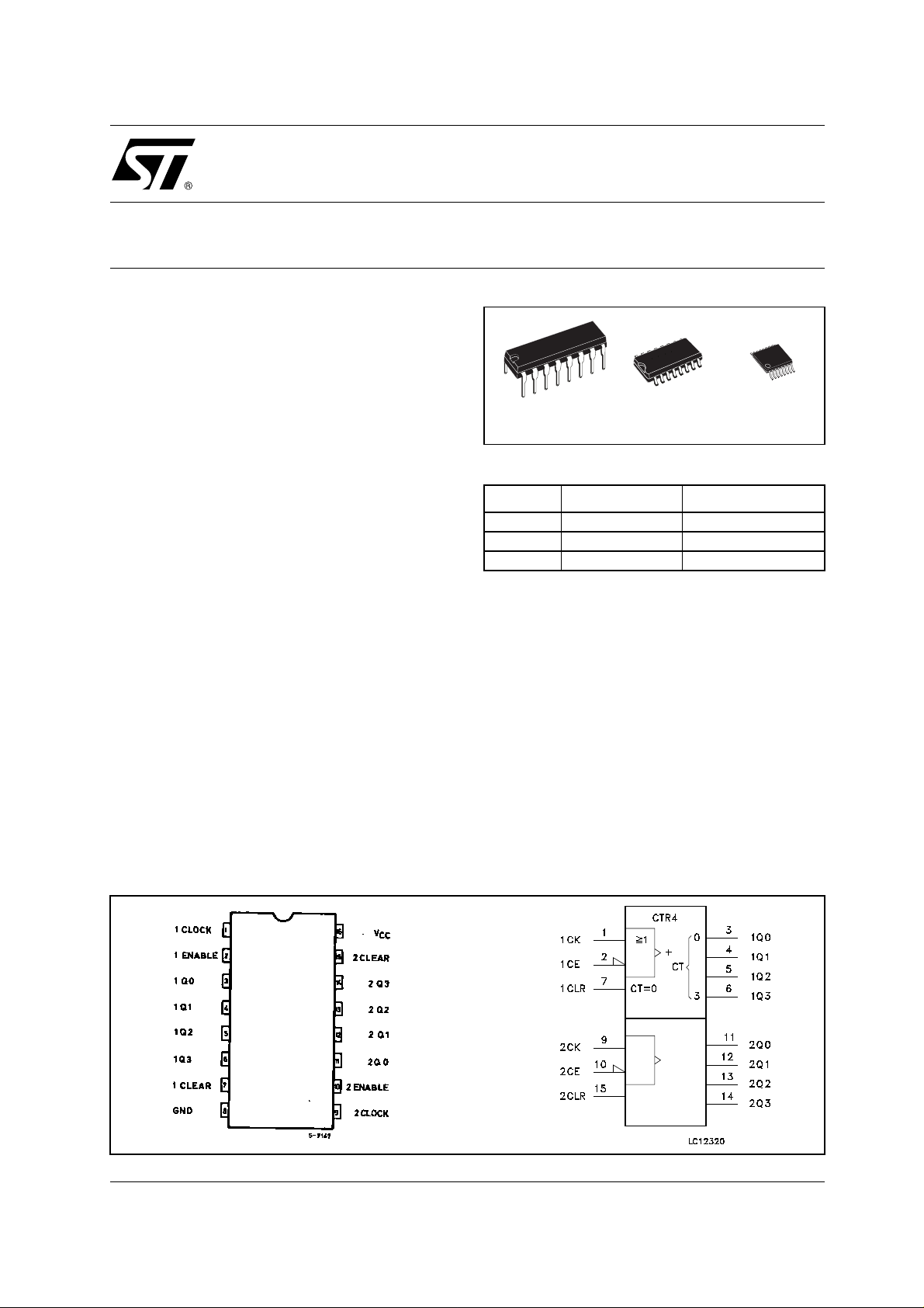
TSSOPDIP SOP
ORDER CODES
PACKAGE TUBE T & R
DIP M74HC4520B1R
SOP M74HC4520M1R M74HC4520RM13TR
TSSOP M74HC4520TTR
each positive-going t ransition of the CLOCK. T he
counters are cleared by high levels on their clear
lines.
The counter can be cascaded in the ripple mode
by connecting Q4 to the enable input of the
subsequent counter while the clock input of the
latter is held permanently low.
All inputs are equipped with protection circuits
against static discharge and transient excess
voltage.
PIN CONNECTION AND IEC LOGIC SYMBOLS
1/12July 2001
M74HC4520
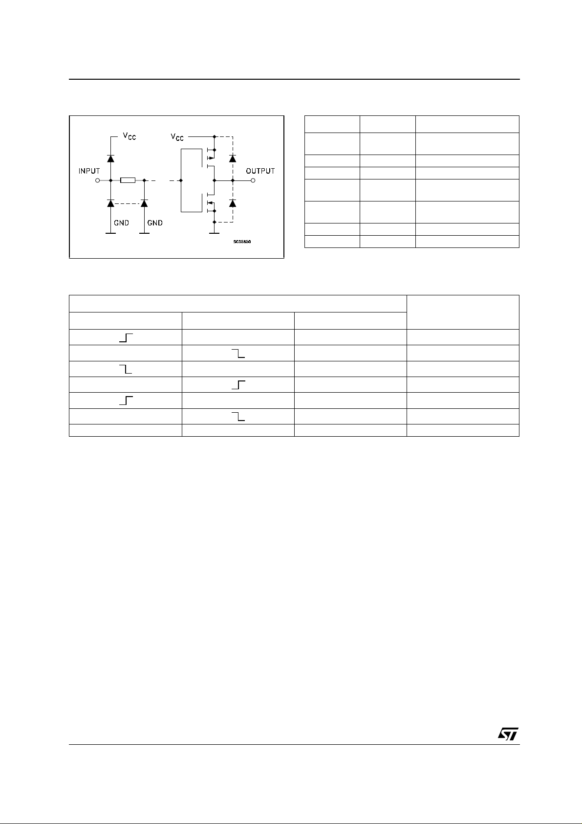
INPUT AND OUTPUT EQUIVALENT CIRCUIT PIN DESCRIPTION
PIN No SYMBOL NAME AND FUNCTION
1, 9
2, 10 1CE, 2CE Clock Enable Inputs
3, 4, 5, 6 1Q0 to 1Q3 Data Outputs
7, 15
11, 12, 13,
14
8 GND Ground (0V)
16 Vcc Positive Supply Voltage
TRUTH TABLE
1CLOCK,
2CLOCK
1CLEAR,
2CLEAR
2Q0 tO 2Q3 Data Outputs
Clock Inputs (LOW to
HIGH, Edge-Triggered)
Asynchronous Reset
Inputs (Active LOW)
CLOCK CLOCK ENABLE CLEAR
L L INCREMENT COUNTER
X L NO CHANGE
H L NO CHANGE
X X H Q0 THRU Q3=L
X : Don’t Care
Z : High Impedance
INPUTS
FUNCTION
H L INCREMENT COUNTER
X L NO CHANGE
L L NO CHANGE
2/12
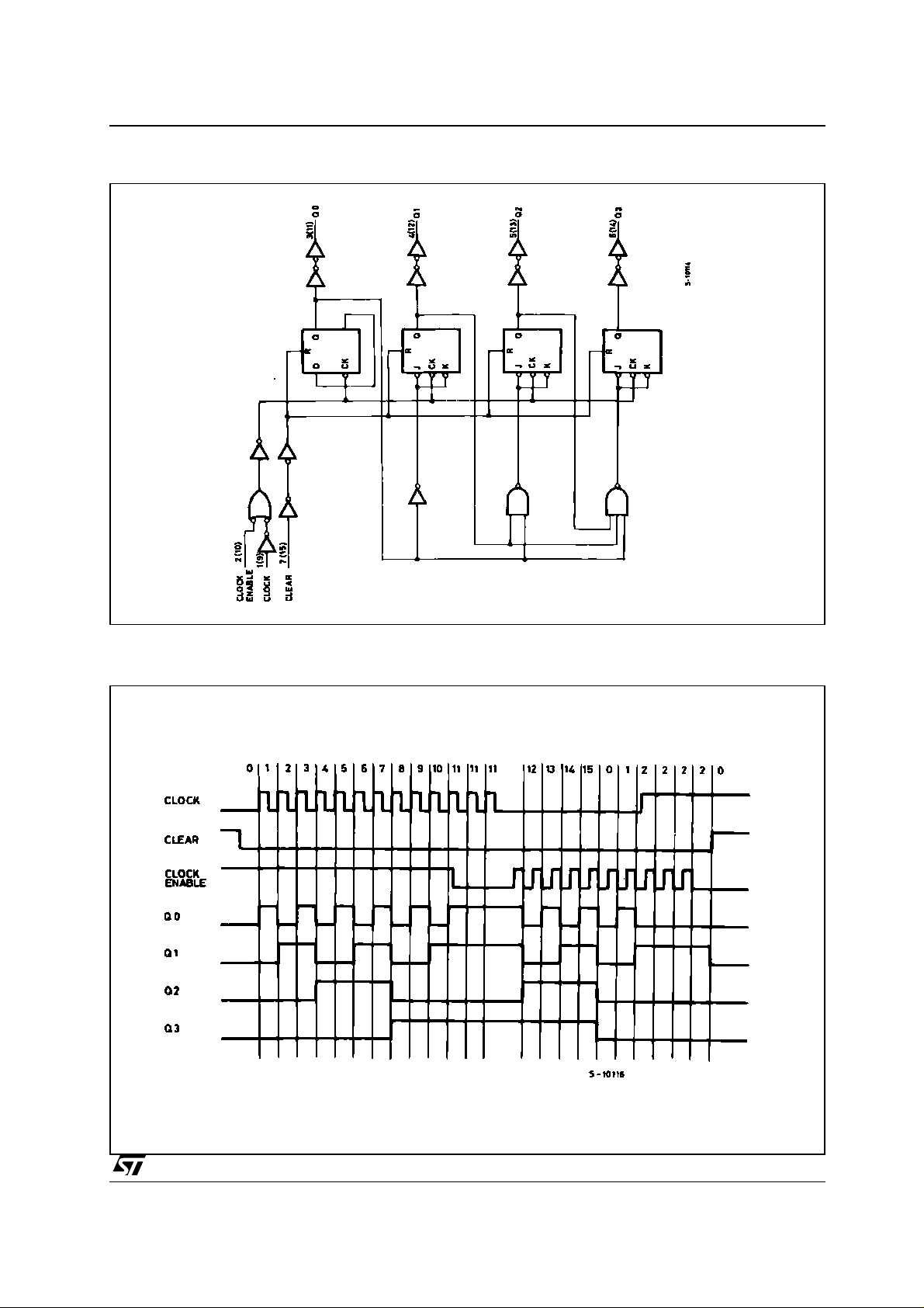
LOGIC DIAGRAM
M74HC4520
This log i c diagram has not be used to est i m at e propagation delays
TIMING CHART
3/12
M74HC4520
ABSOLUTE MAXIMUM RATINGS
Symbol Parameter Value Unit
V
V
V
I
I
OK
I
I
or I
CC
P
T
T
Absolute Maximum Ratings are those values beyond which damage to the device may occur. Functional operation under these conditions is
not implied
(*) 500mW at 65
RECOMMENDED OPERATING CONDITIONS
Symbol Parameter Value Unit
V
V
V
T
t
r
Supply Voltage
CC
DC Input Voltage -0.5 to VCC + 0.5
I
DC Output Voltage -0.5 to VCC + 0.5
O
DC Input Diode Current
IK
DC Output Diode Current
DC Output Current
O
DC VCC or Ground Current
GND
Power Dissipation
D
Storage Temperature
stg
Lead Temperature (10 sec)
L
°C; derate to 300mW by 10mW/°C from 65°C to 85°C
Supply Voltage
CC
Input Voltage 0 to V
I
Output Voltage 0 to V
O
Operating Temperature
op
Input Rise and Fall Time VCC = 2.0V
, t
f
V
V
CC
CC
= 4.5V
= 6.0V
-0.5 to +7 V
± 20 mA
± 20 mA
± 25 mA
± 50 mA
500(*) mW
-65 to +150 °C
300 °C
2 to 6 V
CC
CC
-55 to 125 °C
0 to 1000 ns
0 to 500 ns
0 to 400 ns
V
V
V
V
4/12
 Loading...