

ST M74HC4316 User Manual
M74HC4316
QUAD BILATERAL SWITCH
■ HIGH SPEED:
t
= 13ns (TYP.) at VCC = 6V
PD
■ LOW POWER DISSIPATION:
I
= 1µA(MAX.) at Vcc = 5V
CC
■ LOW "ON" RESISTANCE:
120Ω TY P. (V
50Ω TY P. (V
35Ω TY P. (V
■ WIDE ANALOG INPUT VOLTAGE
RANGE
■ LOW CROSSTALK BETWEEN SWITCHES
■ FA ST SWITCHING
■ SINE WAVE DISTORTION:
± 6v
0.020 at V
■ HIGH NOISE IMMUNITY:
V
= V
NIH
■ PIN AND FUNCTION COMPATIBLE WITH
NIL
- VEE = 2V)
CC
- VEE = 4.5V)
CC
- VEE = 9V)
CC
- VEE = 9V
CC
= 28 % VCC (MIN.)
74 SERIES 4316
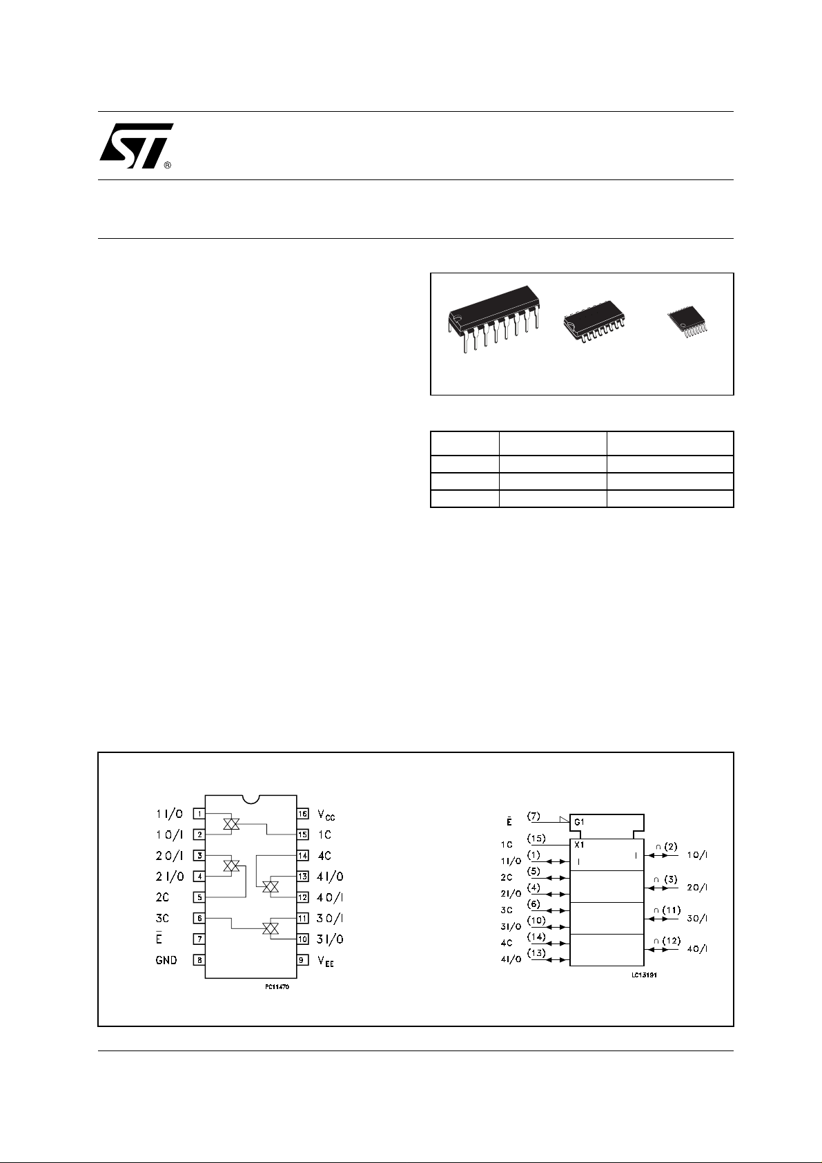
DESCRIPTION
The M74HC4316 is an high speed CMOS QUAD
BILATERAL SW ITCH fabricated with silicon gate
2
C
MOS technology.
This device has four independent analogue
switches. Each switch has two input/output
terminals (nI/O, nO/I) and an active high select
input (nC).
TSSOPDIP SOP
ORDER CODES
PACKAGE TUBE T & R
DIP M74HC4316B1R
SOP M74HC4316M1R M74HC4316RM13TR
TSSOP M74HC4316TTR
When the enable input is high, all four analog
switches are off. The supply vol tage for the dig ital
signals applied to V
and GND must be whitin
CC
the range 0 to 6 V. The voltage swing on the
analogue Inputs/Outputs can be between V
(positive limit) and V
voltage betwee n V
CC
(negative limit). The
EE
and VEE must not exceed
CC
12V.
All inputs are equipped with protection circuits
against static discharge and transient excess
voltage.
PIN CONNECTION AND IEC LOGIC SYM BOLS
1/11July 2001

M74HC4316
LOGIC DIAGRAM PIN DESCRIPTION
PIN No SYMBOL NAME AND FUNCTION
1, 4, 10, 13 1 to 4 I/O Independent Inputs/Out-
2, 3, 11, 12 1 to 4 O/I Independent Outputs/
7E
15, 5, 6, 14 1C to 4C Enable Inputs (Active
9V
8 GND Ground (0V)
16 V
TRUTH TABLE
EE
CC
puts
Inputs
Enable Inputs (Active
LOW)
High)
Negative Supply Voltage
Positive Supply Voltage
E
C SWITCH FUNCTION
LH ON
L L OFF
H X OFF
ABSOLUTE MAXIMUM RATINGS
Symbol Parameter Value Unit
V
V
- VEESupply Voltage
CC
V
V
I
I
OK
I
I
or I
CC
P
T
T
Absolute Maximum Ratings are those values beyond which damage to the device may occur. Functional operation under these conditions is
not implied
(*) 500mW at 65
Supply Voltage
CC
Control Input Voltage -0.5 to VCC + 0.5
I
Switch Input/Output Voltage V
I/O
DC Input Diode Current
IK
EE
DC Output Diode Current
DC Output Source Sink Current Per Output Pin
O
DC VCC or Ground Current
GND
Power Dissipation
D
Storage Temperature
stg
Lead Temperature (10 sec)
L
°C; derate to 300mW by 10mW/°C from 65°C to 85°C
-0.5 to +7 V
-0.5 to +13 V
-0.5 to VCC + 0.5
± 20 mA
± 20 mA
± 25 mA
± 50 mA
500(*) mW
-65 to +150 °C
300 °C
V
V
2/11
M74HC4316
RECOMMENDED OPERATING CONDITIONS
Symbol Parameter Value Unit
V
V
V
- VEESupply Voltage
CC
V
V
T
t
r
DC SPECIFICATIONS
Symbol Parameter
V
IHC
V
ILC
R
ON
∆R
ON
I
OFF
I
IZ
I
IN
Supply Voltage
CC
Supply Voltage
EE
Input Voltage 0 to V
I
Switch I/O Voltage 0 to V
I/O
Operating Temperature
op
Input Rise and Fall Time VCC = 2.0V
, t
f
V
V
CC
CC
= 4.5V
= 6.0V
Test Condition Value
T
= 25°C
A
Min. Typ. Max. Min. Max. Min. Max.
High Level
V
V
CC
EE
(V)
(V)
2.0 1.5 1.5 1.5
Control Input
Voltage
Low Level Control
6.0 4.2 4.2 4.2
2.0 0.5 0.5 0.5
Input Voltage
6.0 1.8 1.8 1.8
ON Resistance 4.5 GND
4.5 -4.5 50 85 105
6.0 -6.0 30 70 85
2.0 GND
4.5 GND 50 80 100
4.5 -4.5 35 60 75
6.0 -6.0 20 40 60
Difference of ON
4.5 GND VIN = V
Resistance
between switches
Input/Output
6.0 -6.0 5 10 15
6.0 GND VOS= VCC or GND
Leakage Current
(SWITCH OFF)
Switch Input
6.0 -6.0
6.0 GND
Leakage Current
(SWITCH ON,
6.0 -6.0
OUTPUT OPEN)
Control Input
6.0
Current
= V
V
I
V
= VCC to VEE
I/O
I
= 0.1mA
I/O
V
= V
I
V
= VCC or VEE
I/O
I
= 0.1mA
I/O
IHC
V
= VCC to VEE
I/O
I
= 0.1mA
I/O
V
= VCC or GND
IS
V
= V
IN
IHC
V
= VCC or GND
OS
= V
V
IN
IHC
V
= VCC or GND
I
IHC
IHC
or V
or V
or V
ILC
ILC
ILC
70 170 200
120 180 215
10 15 20
±0.06 ± 0.6 ± 2
± 0.1 ± 1 ± 2
±0.06 ± 0.6 ± 2 µA
± 0.1 ± 1 ± 2
-5
10
± 0.1 ± 1 ± 1 µA
2 to 12 V
-6 to 0 V
2 to 12 V
CC
CC
-55 to 125 °C
0 to 1000
0 to 500
0 to 400
-40 to 85°C -55 to 125°C
V
V
ns
Unit
V4.5 3.15 3.15 3.15
V4.5 1.35 1.35 1.35
Ω
Ω4.5 -4.5 5 10 15
µA
3/11

M74HC4316
AC ELECTRICAL CHARACTERISTICS (CL = 50 pF, Input tr = tf = 6ns)
Test Condition Value
T
Symbol Par ameter
Φ
Phase Difference
I/O
Between Input
and Output
Output Enable
t
PZL
Time
t
PZH
t
PLZ
t
PHZ
f
MAX
, C - OUT)
(E
Output Disable
Time
, C - OUT)
(E
Maximum Control
Input Frequency
V
V
CC
EE
(V)
(V)
2.0 GND 12 30 40
4.5 GND 3 6 8
6.0 GND 3 5 7
4.5 -4.5 2 4 5
6.0 -6.0 2 4 5
2.0 GND
4.5 GND 14 23 29
R
6.0 GND 12 20 25
= 1KΩ
L
4.5 -4.5 13 21 26
6.0 -6.0 11 18 23
2.0 GND
4.5 GND 28 41 51
R
6.0 GND 24 35 43
= 1KΩ
L
4.5 -4.5 24 34 43
6.0 -6.0 21 29 36
2.0 GND
6.0 GND 1 1
V
R
C
OUT
= 1KΩ
L
= 15 pF
L
= 1/2 V
CC
= 25°C
A
Min. Typ. Max. Min. Max. Min. Max.
56 115 145
112 205 255
2
-40 to 85°C -55 to 125°C
Unit
ns
ns
ns
MHz4.5 GND 9
CAPACITIVE CHARACTERISTICS
Test Condition Value
T
Symbol Parameter
V
CC
(V)
C
C
C
C
Input Capacitanc e 5 10 10 10 pF
IN
Switch Terminal
I/O
Capacitance
Feed Through
IOS
Capacitanc e
Power Dissipation
PD
Capacitance
4.5
4.5
5.0
-4.5
-4.5
GND
= 25°C
A
Min. Typ. Max. Min. Max. Min. Max.
5pF
1pF
16 pF
(note 1)
1) CPD is defined as the value of the IC’s internal equivalent capacitance which is calculated from the operating current consumption without
load. (R ef er to Test Circui t). Averag e operating current can be obtained by the following equation. I
-40 to 85°C -55 to 125°C
= CPD x VCC x fIN + ICC
CC(opr)
Unit
4/11
 Loading...