

8 BIT SIPO SHIFT LATCH REGISTER (3-STATE)
■ HIGH SPEED :
f
=80MHz(TYP.)atVCC=6V
MAX
■ LOW POWER DISSIPATION:
I
=4µA(MAX.) at TA=25°C
CC
■ HIGH NOISE IMMUNITY:
V
NIH=VNIL
■ SYMMETRICAL OUTPUT IMPEDANCE:
|I
|=IOL=4mA(MIN)
OH
■ BALANCED PROPAGATION DELAYS:
≅ t
t
PLH
■ WIDE OPERATING VOLTAGE RANGE:
V
(OPR) = 2 V to 6V
CC
■ PIN AND FUNCTION COMPATIBLE WITH
74 SERIES 4094
DESCRIPTION
The M74HC4094 is an high speed CMOS 8 BIT
SIPO SHIFT LATCH REGISTER fabricated with
silicon gate C
This device consists of an 8 bit shift register and
an 8 bit latch with 3 state output buffer. Data is
shifted serially trough the shift register on the
positive going transition of the clock input signal.
Theoutputofthelaststage(Qs)canbeusedto
cascade several devices.
Data on the Qs out put is transferred to a second
output (Qs’) on the following negative transition of
=28%VCC(MIN.)
PHL
2
MOS technology.
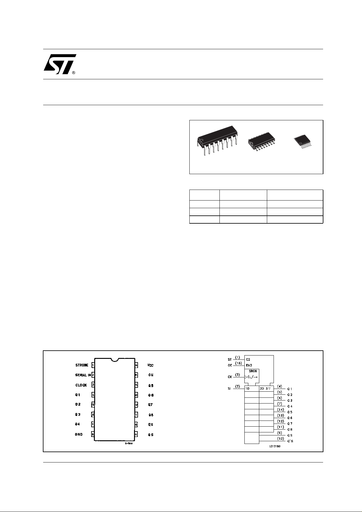
M74HC4094
TSSOPDIP SOP
ORDER CODES
PACKAGE TUBE T & R
DIP M74HC4094B1R
SOP M74HC4094M1R M74HC4094RM13TR
TSSOP M74HC4094TTR
the clock input sig nal. The data of each stage of
the s hift register is provided with a latch, which
latches data on the negativ e going transition of the
STROBE input signal. When the STROBE input is
held high, data propagates through the latch to a
3-state output buffer.
This buffer is enabled when OUT PUT ENA BLE
input is taken high.
All inputs are equipped with protection circuits
against static discharge and transient excess
voltage.
PIN CONNE CTION AND IEC LOGIC SYMBOLS
1/12January 2003
M74HC4094
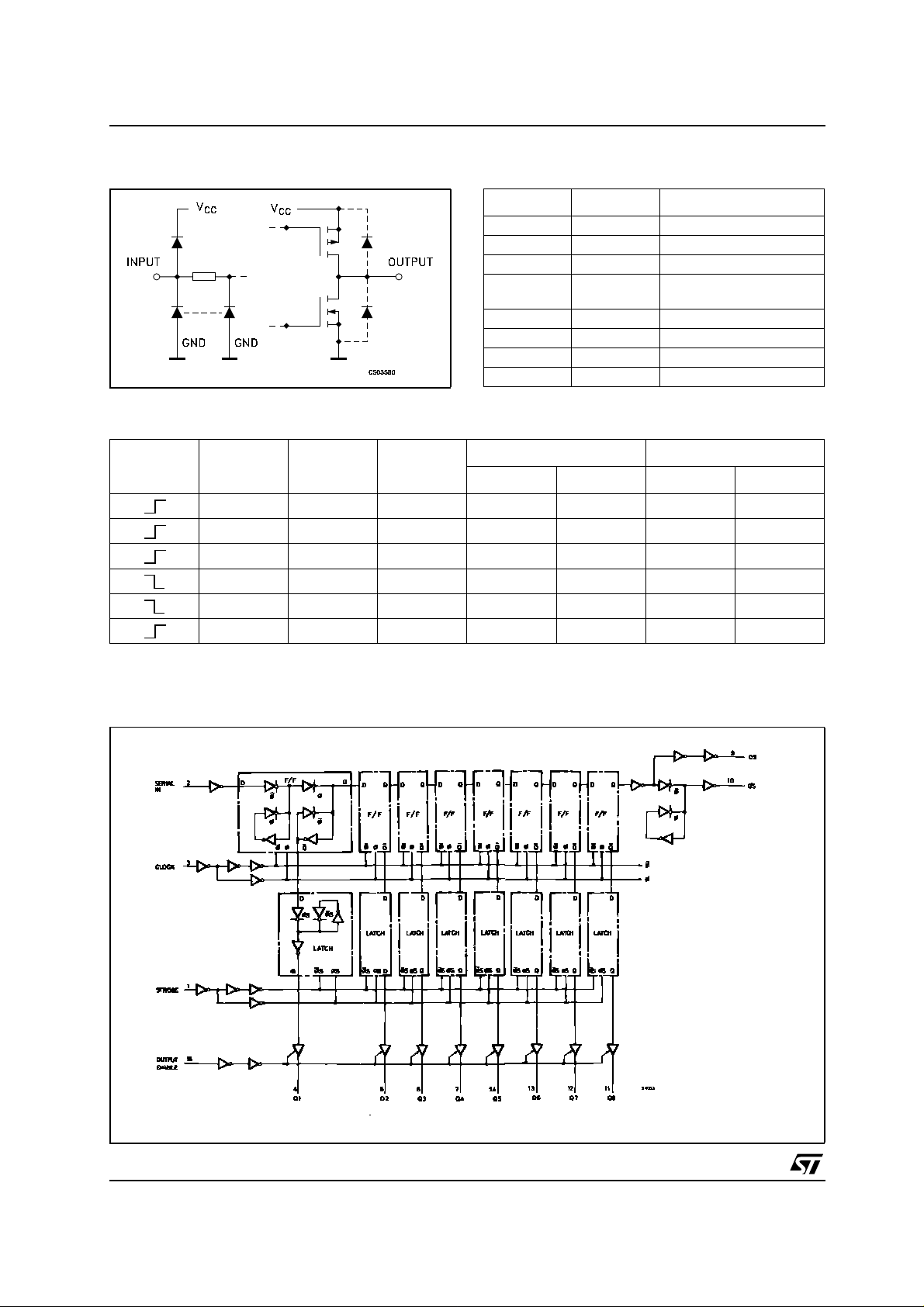
INPUT AND OUTPUT EQUIVALENT CIRCUIT PIN DESCRIPTION
PIN No SYMBOL NAME AND FUNCTION
1 STROBE Strobe Input
2 SERIAL IN Serial Input
3 CLOCK Clock Input
4, 5, 6, 7, 14,
13, 12, 11
9, 10 QS Q’S Serial Outputs
15 OE Output Enable Input
8 GND Ground (0V)
16 Vcc Positive Supply Voltage
TRUTH TABLE
Q1 to Q7 Parallel Outputs
CK OE ST SI
H H L L Qn-1 Q7 NC
HHHHQn-1 Q7 NC
HLXNCNCQ7NC
LXXZZNCQ8
H H H NC NC NC Q8
LXXZZQ7NC
X : Don’t Care
Z : High Impedance
NC: NoChange
LOGIC DIAGRAM
PARALLEL OUTPUTS SERIAL OUTPUTS
Q1 Qn Qs Qs’
This logic diagram has not be used to estimate propagation delays
2/12

TIMING CHART
M74HC4094
ABSOLUTE MAXIMUM RATINGS
Symbol Parameter Value Unit
V
CC
V
V
I
IK
I
OK
I
or I
I
CC
P
T
stg
T
Absolute Maximum Ratings are those values beyond which damage to the device may occur. Functional operation under these conditions is
not implied
(*) 500mWat 65
Supply Voltage
DC Input Voltage -0.5 to VCC+ 0.5
I
DC Output Voltage -0.5 to VCC+ 0.5
O
DC Input Diode Current
DC Output Diode Current
DC Output Current
O
DC VCCor Ground Current
GND
Power Dissipation
D
Storage Temperature
Lead Temperature (10 sec)
L
°C; derate to 300mW by 10mW/°Cfrom65°Cto85°C
-0.5 to +7 V
V
V
± 20 mA
± 20 mA
± 25 mA
± 50 mA
500(*) mW
-65 to +150 °C
300 °C
3/12
M74HC4094
RECOMMENDED OPERATING CONDITIONS
Symbol Parameter Value Unit
V
CC
V
V
T
t
r,tf
DC SPECIFICATIONS
Symbol Parameter
V
IH
V
IL
V
OH
V
OL
I
I
I
OZ
I
CC
Supply Voltage
Input Voltage 0 to V
I
Output Voltage 0 to V
O
Operating Temperature
op
Input Rise and Fall Time VCC= 2.0V
= 4.5V
V
CC
= 6.0V
V
CC
Test Condition Value
= 25°C
T
A
Min. Typ. Max. Min. Max. Min. Max.
High Level Input
V
CC
(V)
2.0 1.5 1.5 1.5
Voltage
6.0 4.2 4.2 4.2
Low Level Input
2.0 0.5 0.5 0.5
Voltage
6.0 1.8 1.8 1.8
High Level Output
Voltage
Low Level Output
Voltage
Input Leakage
Current
High Impedance
Output Leakage
Current
Quiescent Supply
Current
2.0
4.5
6.0
4.5
6.0
2.0
4.5
6.0
4.5
6.0
6.0
6.0
6.0
IO=-20 µA
I
=-20 µA
O
=-20 µA
I
O
=-4.0 mA
I
O
=-5.2 mA
I
O
IO=20 µA
I
=20 µA
O
=20 µA
I
O
=4.0 mA
I
O
=5.2 mA
I
O
I=VIH
or GND
or V
IL
V
I=VCC
V
VO=VCCor GND
V
I=VCC
or GND
1.9 2.0 1.9 1.9
4.4 4.5 4.4 4.4
5.9 6.0 5.9 5.9
4.18 4.31 4.13 4.10
5.68 5.8 5.63 5.60
0.0 0.1 0.1 0.1
0.0 0.1 0.1 0.1
0.0 0.1 0.1 0.1
0.17 0.26 0.33 0.40
0.18 0.26 0.33 0.40
± 0.1 ± 1 ± 1 µA
± 0.5 ± 5 ± 10 µA
44080µA
2to6 V
CC
CC
-55 to 125 °C
0 to 1000 ns
0 to 500 ns
0 to 400 ns
-40 to 85°C -55 to 125°C
V
V
Unit
V4.5 3.15 3.15 3.15
V4.5 1.35 1.35 1.35
V
V
4/12
 Loading...