

M74HC4066
QUAD BILATERAL SWITCH
■ HIGH SPEED:
t
= 7ns (TYP.) at VCC = 6V
PD
■ LOW POWER DISSIPATION:
I
= 1µA(MAX.) at TA=25°C
CC
■ LOW "ON" RESISTANCE:
R
= 50Ω TYP. AT VCC = 9V, I
ON
■ WIDE OPERATING VOLTAGE RANGE
V
(OPR) = 2V TO 12V
CC
■ SINE WAVE DISTORTION:
0.042% at V
■ HIGH NOISE IMMUNITY:
V
= V
NIH
■ PIN AND FUNCTION COMPATIBLE WITH
= 4V f = 1KHz
CC
= 28 % VCC (MIN.)
NIL
= 100 µA
I/O
74 SERIES 4066
DESCRIPTION
The M74HC4066 is an high speed CMOS QUAD
BILATERAL SW ITCH fabricated with silicon gate
2
C
MOS technology.
TSSOPDIP SOP
ORDER CODES
PACKAGE TUBE T & R
DIP M74HC4066B1R
SOP M74HC4066M1R M74HC4066RM13TR
TSSOP M74HC4066TTR
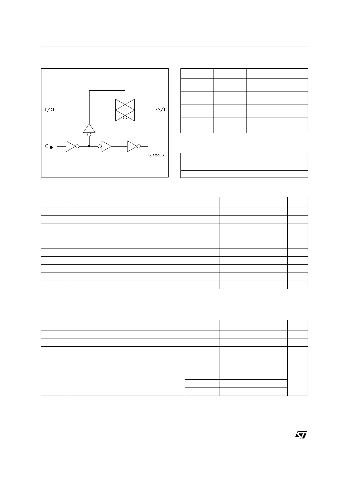
The C input is provided to control the switch; the
switch is on when the C input is held high and off
when C is held low.
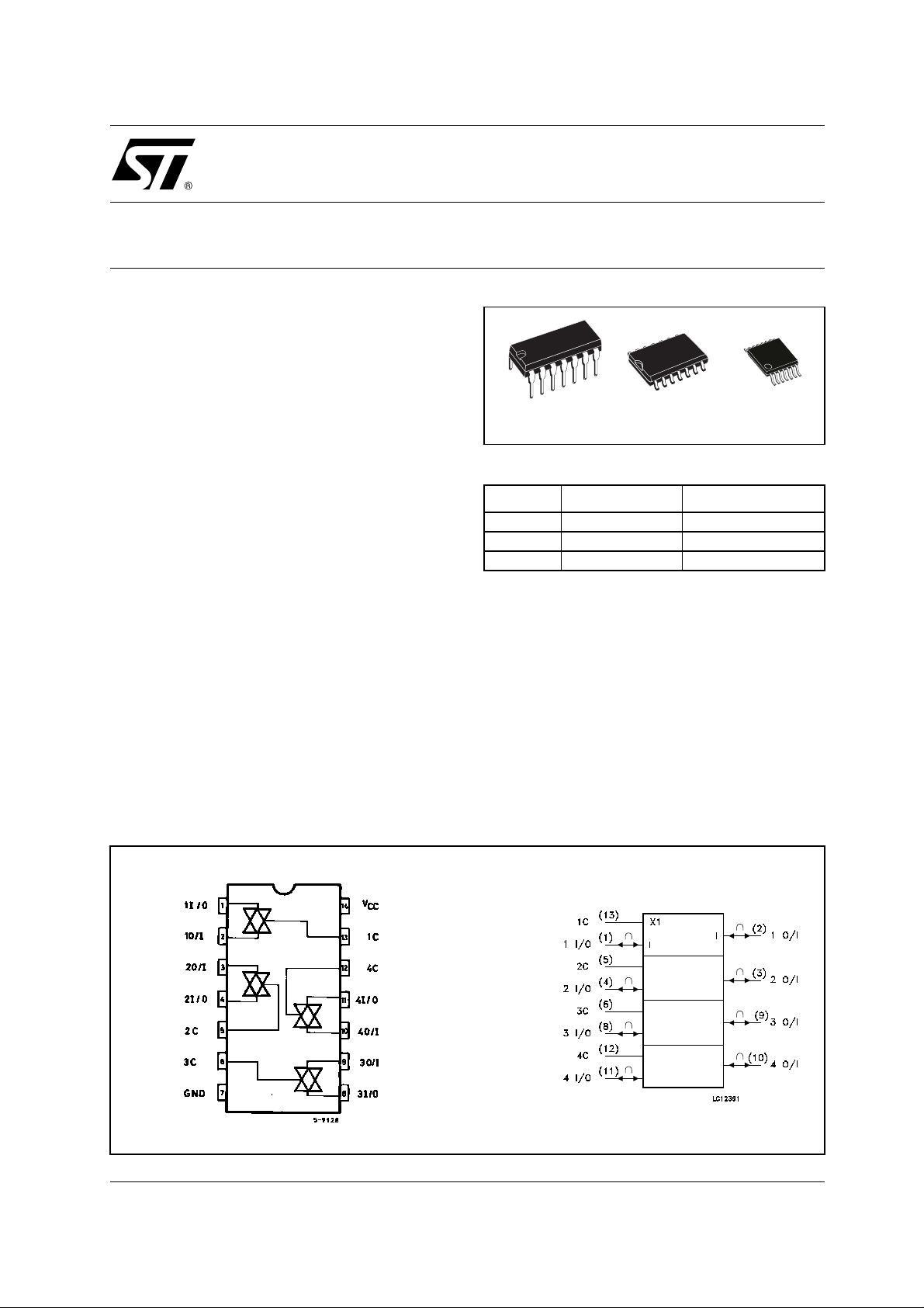
PIN CONNECTION AND IEC LOGIC SYM BOLS
1/11July 2001
M74HC4066
LOGIC DIAGRAM PIN DESCRIPTION
PIN No SYMBOL NAME AND FUNCTION
1, 4, 8, 11 1 to 4 I/O Independent Inputs/Out-
2, 3, 9, 10 1 to 4 O/I Independent Outputs/
13, 5, 6, 12 1C to 4C Enable Inputs (Active
7 GND Ground (0V)
14 V
CC
TRUTH TABLE
CONTROL SWITCH FUNCTION
HON
LOFF
ABSOLUTE MAXIMUM RATINGS
Symbol Parameter Value Unit
V
V
V
I
OK
I
IOK
I
I
or I
CC
P
T
T
Absolute Maximum Ratings are those values beyond which damage to the device may occur. Functional operation under these conditions is
not implied
(*) 500mW at 65
Supply Voltage
CC
DC Input Voltage -0.5 to VCC + 0.5
IN
DC Input/Output Voltage -0.5 to VCC + 0.5
I/O
Control Input DC Diode Current
I/O DC Diode Current
DC Output Source Sink Current Per Output Pin
O
DC VCC or Ground Current
GND
Power Dissipation
D
Storage Temperature
stg
Lead Temperature (10 sec)
L
°C; derate to 300mW by 10mW/°C from 65°C to 85°C
puts
Inputs
High)
Positive Supply Voltage
-0.5 to +13 V
V
V
± 20 mA
± 20 mA
± 25 mA
± 50 mA
500(*) mW
-65 to +150 °C
300 °C
RECOMMENDED OPERATING CONDITIONS
Symbol Parameter Value Unit
2/11
V
V
V
T
t
r
Supply Voltage
CC
Input Voltage (Control) 0 to V
IN
I/O Voltage 0 to V
I/O
Operating Temperature
op
Input Rise and Fall Time VCC = 2.0V
V
= 4.5V
, t
f
CC
V
CC
V
CC
= 6.0V
= 10.0V
2 to 12 V
CC
CC
-55 to 125 °C
0 to 1000
0 to 500
0 to 400
0 to 250
V
V
ns
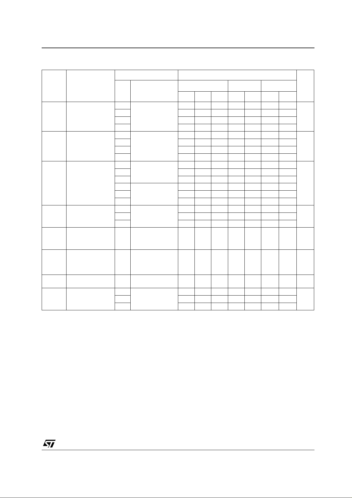
DC SPECIFICATIONS
Symbol Parameter
V
V
R
∆R
I
High Level Control
IHC
Input Voltage
Low Level Control
ILC
Input Voltage
ON Resistance 4.5 VI = V
ON
Difference of ON
ON
Resistance
between switches
Input/Output
OFF
Leakage Current
(SWITCH OFF)
I
Switch Input
IZ
Leakage Current
(SWITCH ON,
OUTPUT OPEN)
I
Control Input
IN
Current
I
Quiescent Supply
CC
Current
M74HC4066
Test Condition Value
T
= 25°C
V
CC
(V)
A
Min. Typ. Max. Min. Max. Min. Max.
2.0 1.5 1.5 1 .5
4.5 3.15 3.15 3.15
9.0 6.3 6.3 6 .3
12.0 8.4 8.4 8 .4
2.0 0.5 0.5 0.5
4.5 1.35 1.35 1.35
9.0 2.7 2.7 2.7
12.0 3.6 3.6 3.6
V
9.0 55 85 100 150
I/O
12.0 45 80 90 120
4.5
V
9.0 50 75 95 115
I/O
12.0 45 70 90 110
4.5
V
9.0 5
I/O
12.0 5
IHC
= VCC to GND
I
≤ 1mA
I/O
= V
V
I
IHC
= VCC or GND
I
≤ 1mA
I/O
= V
V
I
IHC
= VCC or GND
I
≤ 1mA
I/O
96 170 200 250
70 100 130 160
10
VOS = VCC or GND
V
12.0
12.0
6.0
= VCC or GND
IS
V
= V
IN
= VCC or GND
V
OS
V
= V
IN
V
= VCC or GND
I
ILC
IHC
6.0
V
= VCC or GND
I
12.0 8 80 160
-40 to 85°C -55 to 125°C
± 0.1 ± 1 ± 2 µA
± 0.1 ± 1 ± 2 µA
± 0.1 ± 1 ± 1 µA
11020
Unit
V
V
Ω
Ω
µA9.0 4 40 80
3/11
M74HC4066
AC ELECTRICAL CHARACTERISTICS (CL = 50 pF, Input tr = tf = 6ns)
Test Condition Value
T
Symbol Parameter
Φ
Phase Difference
I/O
Between Input and
Output
t
t
t
t
Output Enable Time 2.0
PZL
PZH
Output Disable
PLZ
Time
PHZ
Maximum Control
Input Frequency
V
CC
(V)
2.0 10 50 65 75
4.5 4 10 13 15
9.0 3 8 10 13
12.0 3 7 9 10
4.5 8 20 25 30
9.0 6 12 22 27
R
= 1KΩ
L
12.0 6 12 18 25
2.0
4.5 10 23 29 35
9.0 8 20 25 30
R
= 1KΩ
L
12.0 8 18 22 27
2.0
4.5 30
9.0 30
12.0 30
= 1KΩ
R
L
CL = 15 pF
V
= 1/2 V
OUT
CC
= 25°C
A
Min. Typ. Max. Min. Max. Min. Max.
18 100 125 150
20 115 145 175
30
-40 to 85°C -55 to 125°C
Unit
ns
ns
ns
MHz
CAPACITIVE CHARACTERISTICS
Test Condition Value
= 25°C
Symbol Parameter
V
CC
(V)
C
Input Capacitanc e 5 10 10 1 0 pF
IN
C
C
C
Switch Terminal
I/O
Capacitance
Feed Through
IOS
Capacitanc e
Power Dissipation
PD
Capacitance
T
A
Min. Typ. Max. Min. Max. Min. Max.
6pF
0.5 pF
15 pF
(note 1)
1) CPD is defined as the value of the IC’s internal equivalent capacitance which is calculated from the operating current consumption without
load. (R ef er to Test Circ ui t ). Average operating current can be obtained by t he following equation. I
-40 to 85°C -55 to 125°C
= CPD x VCC x fIN + ICC
CC(opr)
Unit
4/11

M74HC4066
ANALOG SWITCH CHARACTERISTICS (GND = 0V;TA = 25°C)
Symbol Parameter Test Condition Value Unit
f
MAX
Sine Wave
Distortion (THD)
Frequency
Response
(Switch ON)
Feed through
Attenuation (Switch
OFF)
Crosstalk (Control
Input to Signal
Output)
Crosstalk (Between
Any Switches)
V
V
CC
(V)
4.5 4
9.0 8 0.04
4.5 Adjust fIN voltage to obtain 0 dBm at VOS.
9.0 200
4.5 V
9.0 -60
4.5
9.0 100
4.5 Adjust V
9.0 -60
IN
(V
)
p-p
= 1 KHz RL = 10 KΩ, CL = 50 pF
f
IN
Increase f
IN
R
L
= 600Ω, CL = 50 pF, fIN = 1MHz square wave (tr = tf =6ns)
R
L
R
L
Frequency until dB meter reads -3dB
IN
= 50Ω, CL = 10 pF
R
L
is centered at VCC/2. Adjust input for 0 dBm
= 600Ω CL = 50 pF, fIN = 1MHz sine wave
to Obtain 0 dBmat input
IN
= 600Ω, CL = 50 pF, fIN = 1MHz sine wave
Typ.
0.05
200
-60
60
-60
%
MHz
dB
mV
dB
5/11

M74HC4066
SWITCHING CARACTERISTICS TEST CIRCUIT
CROSSTALK (control to output)
CROSSTALK BETWEEN ANY TWO SWITCHES
BANDWIDTH AND FEEDTHROUGH ATTENUATION
MAXIMUM CONTROL FREQUENCY
6/11
M74HC4066
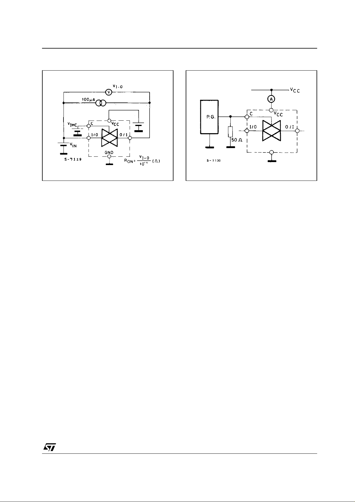
CHANNEL RESISTANCE (R
ICC (Opr.)
ON)
7/11

M74HC4066
Plastic DIP-14 MECHANICAL DATA
mm. inch
DIM.
MIN. TYP MAX. MIN. TYP. M AX.
a1 0.51 0.020
B 1.39 1.65 0.055 0.065
b 0.5 0.020
b1 0.25 0.010
D 20 0.787
E 8.5 0.335
e 2.54 0.100
e3 15.24 0.600
F 7.1 0.280
I 5.1 0.201
L 3.3 0.130
Z 1.27 2.54 0.050 0.100
8/11
P001A

SO-14 MECHANICAL DATA
M74HC4066
DIM.
A 1.75 0.068
a1 0.1 0.2 0.003 0.007
a2 1.65 0.064
b 0.35 0.46 0.013 0.018
b1 0.19 0.25 0.007 0.010
C 0.5 0.019
c1 45° (typ.)
D 8.55 8.75 0.336 0.344
E 5.8 6.2 0.228 0.244
e 1.27 0.050
e3 7.62 0.300
F 3.8 4.0 0.149 0.157
G 4.6 5.3 0.181 0.208
L 0.5 1.27 0.019 0.050
M 0.68 0.026
S8° (max.)
MIN. TYP MAX. MIN. TYP. M AX.
mm. inch
PO13G
9/11

M74HC4066
TSSOP14 MECHANICAL DATA
mm. inch
DIM.
MIN. TYP MAX. MIN. TYP. M AX.
A 1.2 0.047
A1 0.05 0.15 0.002 0.004 0.006
A2 0.8 1 1.05 0.031 0.039 0.041
b 0.19 0.30 0.007 0.012
c 0.09 0.20 0.004 0.0089
D 4.9 5 5.1 0.193 0.197 0.201
E 6.2 6.4 6.6 0.244 0.252 0.260
E1 4.3 4.4 4.48 0.169 0.173 0.176
e 0.65 BSC 0.0256 BSC
K0° 8°0° 8°
L 0.45 0.60 0.75 0.018 0.024 0.030
A2
A
A1
b
e
c
K
L
E
D
E1
PIN 1 IDENTIFICATION
10/11
1
0080337D

M74HC4066
Information furnished is bel ieved to be accurate and reliable. However, STMicroe lectronics assumes no responsibility for the
consequences of use of such information nor for any infringement of patents or other rights of third parties which may result from
its use. No li cense is granted by imp lica tion or otherwise under a ny patent or patent rig hts of STMicroelectronics. Sp ec ificat ions
mentioned in this publication ar e subject to change without notice. This publication supersedes and replaces all information
previously supplied. S TMicroelectronics products are not authorized for use as critica l components in life suppo rt devices or
systems without express written approval of STMicroelectronics.
Australi a - Brazil - Chi na - Finland - F rance - Germ any - Hong Kon g - India - Italy - Japan - Malaysia - Malta - Mo rocco
© The ST logo is a registered trademark of STMicroelectronics
© 2001 STM icroelectronics - Printed in Italy - All Rights Reserv ed
STMicr o el ectronics G ROU P OF COMPANIES
Singapo re - Spain - Sweden - Swit zerland - Uni ted Kingdom
© http://www.st.com
11/11
 Loading...