

M74HC4017
DECADE COUNTER/DIVIDER
■ HIGH SPEED :
t
= 21 ns (TYP.) at VCC = 6V
PD
■ LOW POWER DISSIPATION:
I
=4µA(MAX.) at TA=25°C
CC
■ HIGH NOISE IMMUNITY:
V
= V
NIH
■ SYMMETRICAL OUTPUT IMPEDANCE:
|I
| = IOL = 4mA (MIN)
OH
■ BALANCED PROPAGATION DELAYS:
t
≅ t
PLH
■ WIDE OPERATING VOLTAGE RANGE:
V
(OPR) = 2V to 6V
CC
■ PIN AND FUNCTION COMPATIBLE WITH
= 28 % VCC (MIN.)
NIL
PHL
74 SERIES 4017
DESCRIPTION
The M74HC4017 is an high speed CMOS
DECADE COUNTER/DIVIDER fabricated with
silicon gate C
2
MOS technology.
The M74HC4017 is a 5-stage Johnson counter
with 10 decoded outputs. Each of the decoded
outputs is normally low and sequentially goes high
on the low to high transition of the clock input.
Each output stays high fo r one clock period of t he
10 clock period cycle. The CARRY output goes
low to high after OUTP UT 10 goes low, and can
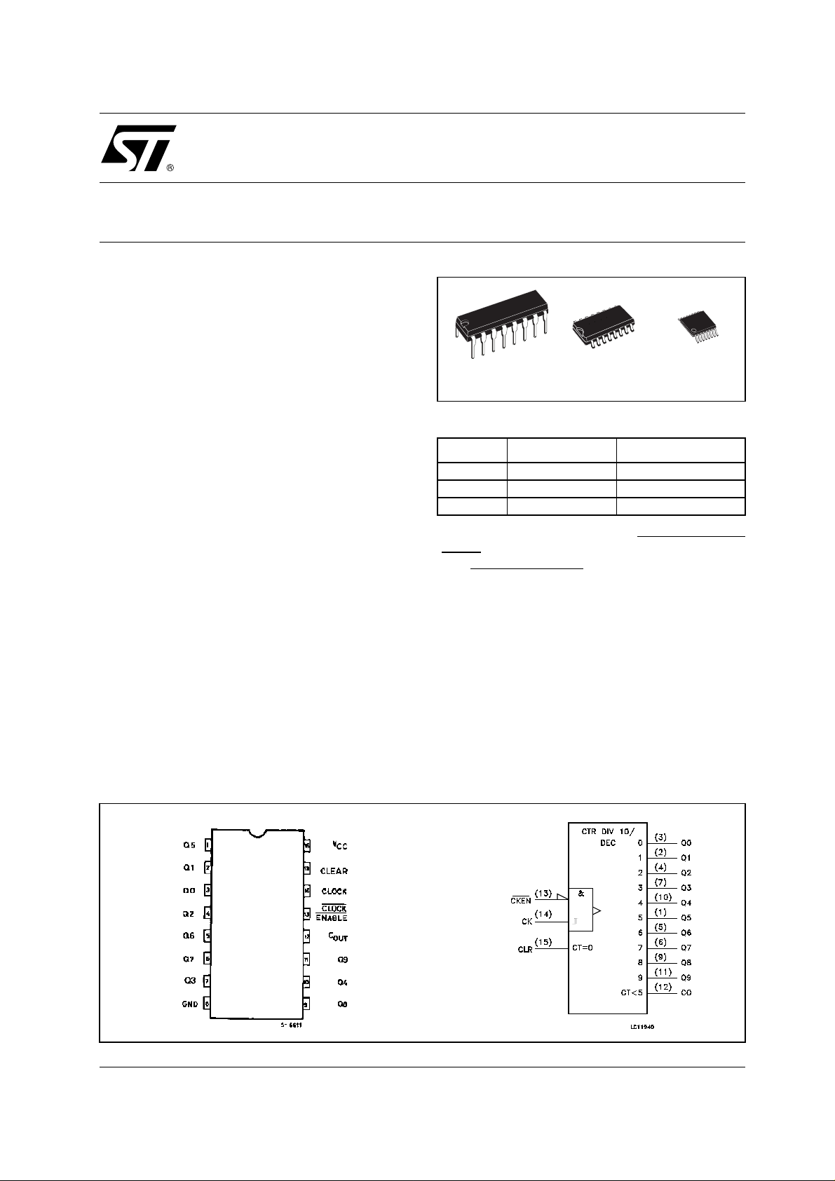
TSSOPDIP SOP
ORDER CODES
PACKAGE TUBE T & R
DIP M74HC4017B1R
SOP M74HC4017M1R M74HC4017RM13TR
TSSOP M74HC4017TTR
be used in conjunction with the CL OCK ENAB LE
(CKEN)to cascade several stages.
The CLOCK ENABLE
input disables counting
when in the high st ate. A CLEAR (CLR) input is
also provided which when taken high sets all the
decoded outputs low.
All inputs are equipped with protection circuits
against static discharge and transient excess
voltage.
PIN CONNECTION AND IEC LOGIC SYMBOLS
1/12August 2001
M74HC4017
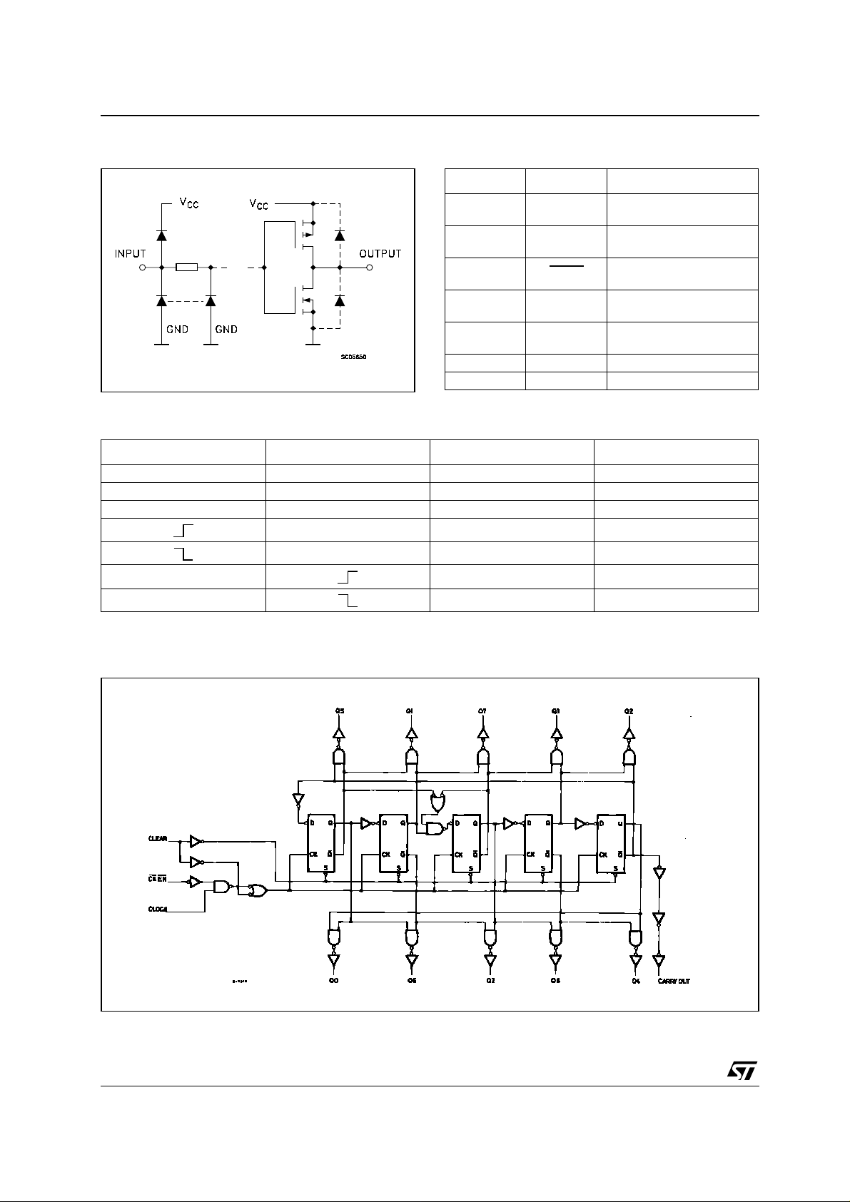
INPUT AND OUTPUT EQUIVALENT CIRCUIT PIN DESCRIPTION
PIN No SYMBOL NAME AND FUNCTION
TRUTH TABLE
CLOCK CLOCK ENABLE CLEAR DECODED OUTPUT(H)
XXHQO
LXLQn
XHLQn
HLQn
H L Qn + 1
X : Don’t Care
Qn : No Ch ange
3, 2, 4, 7, 10,
1, 5, 6, 9, 11
12
13 CKEN
14 CLOCK
15 CL EAR
8 GND Ground (0V)
16 Vcc Positive Supply Voltage
L L Qn + 1
LLQn
Q0 to Q9 Decoded Outputs
C
OUT
Carry Output
(Active LOW)
Clock Enable Input
(Active LOW)
Clock Input (LOW to
HIGH, Edge Triggered)
Master Reset Inputs
(Active HIGH)
LOGIC DIAGRAM
This log i c diagram has not be used to esti m ate propagation delays
2/12
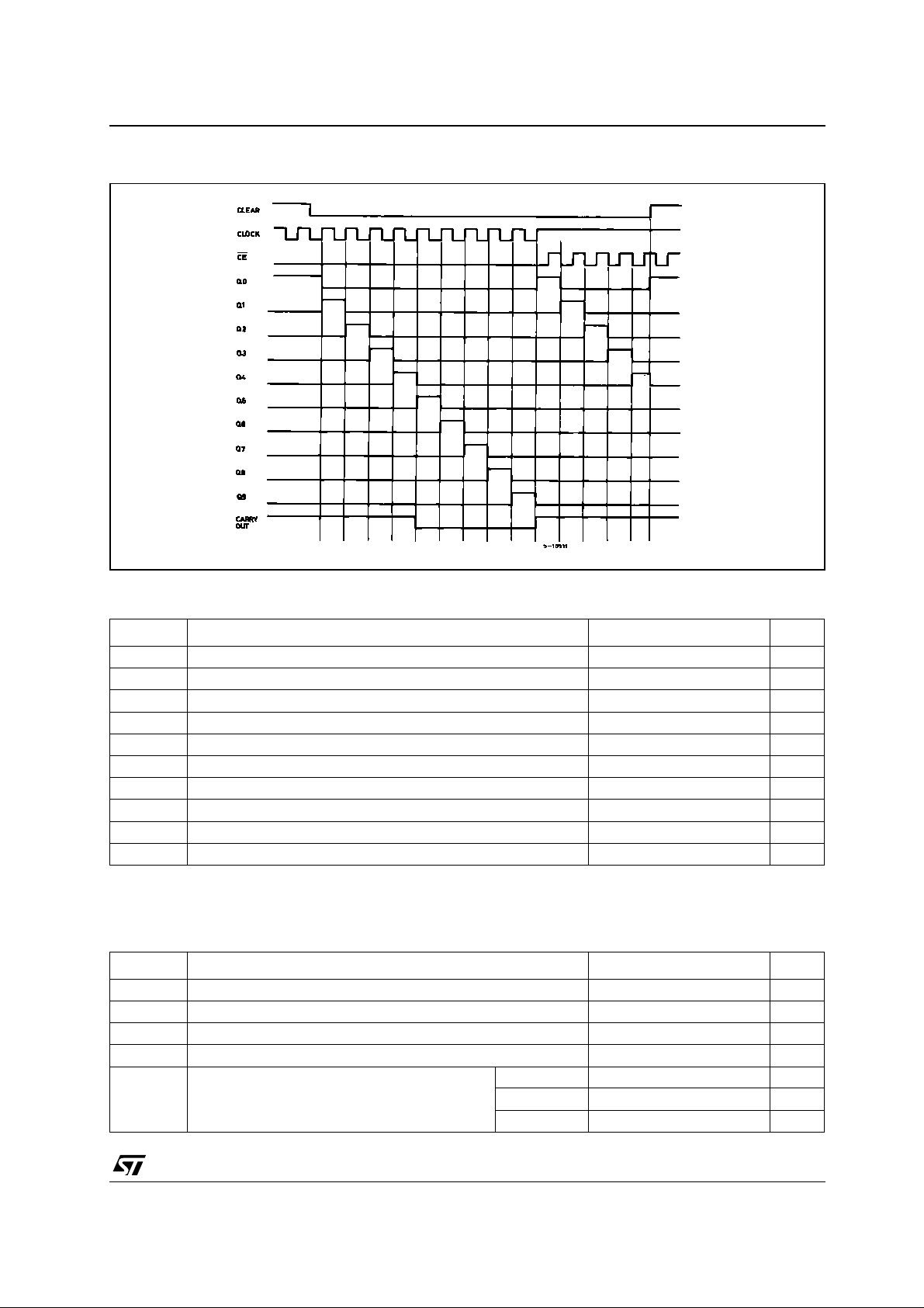
TIMING DIAGRAM
M74HC4017
ABSOLUTE MAXIMUM RATINGS
Symbol Parameter Value Unit
V
V
V
I
I
OK
I
I
or I
CC
P
T
T
Absolute Maximum Ratings are those values beyond which damage to the device may occur. Functional operation under these conditions is
not implied
(*) 500mW at 65
Supply Voltage
CC
DC Input Voltage -0.5 to VCC + 0.5
I
DC Output Voltage -0.5 to VCC + 0.5
O
DC Input Diode Current
IK
DC Output Diode Current
DC Output Current
O
DC VCC or Ground Current
GND
Power Dissipation
D
Storage Temperature
stg
Lead Temperature (10 sec)
L
°C; derate to 300mW by 10mW/°C from 65°C to 85°C
-0.5 to +7 V
V
V
± 20 mA
± 20 mA
± 25 mA
± 50 mA
500(*) mW
-65 to +150 °C
300 °C
RECOMMENDED OPERATING CONDITIONS
Symbol Parameter Value Unit
V
V
V
T
t
r
Supply Voltage
CC
Input Voltage 0 to V
I
Output Voltage 0 to V
O
Operating Temperature
op
Input Rise and Fall Time VCC = 2.0V
, t
f
V
V
CC
CC
= 4.5V
= 6.0V
2 to 6 V
CC
CC
-55 to 125 °C
0 to 1000 ns
0 to 500 ns
0 to 400 ns
V
V
3/12
M74HC4017
DC SPECIFICATIONS
Symbol Parameter
V
V
V
V
I
High Level Input
IH
Voltage
Low Level Input
IL
Voltage
High Level Output
OH
Voltage
Low Level Output
OL
Voltage
I
Input Leakage
I
Current
Quiescent Supply
CC
Current
Test Condition Value
V
(V)
CC
= 25°C
A
Min. Typ. Max. Min. Max. Min. Max.
-40 to 85°C -55 to 125°C
T
2.0 1.5 1.5 1.5
6.0 4.2 4.2 4.2
2.0 0.5 0.5 0.5
6.0 1.8 1.8 1.8
2.0
4.5
6.0
4.5
6.0
2.0
4.5
6.0
4.5
6.0
6.0
6.0
IO=-20 µA
I
=-20 µA
O
I
=-20 µA
O
I
=-4.0 mA
O
I
=-5.2 mA
O
IO=20 µA
I
=20 µA
O
I
=20 µA
O
I
=4.0 mA
O
I
=5.2 mA
O
= VCC or GND
V
I
= VCC or GND
V
I
1.9 2.0 1.9 1.9
4.4 4.5 4.4 4.4
5.9 6.0 5.9 5.9
4.18 4.31 4.13 4.10
5.68 5.8 5.63 5.60
0.0 0.1 0.1 0.1
0.0 0.1 0.1 0.1
0.0 0.1 0.1 0.1
0.17 0.26 0.33 0.40
0.18 0.26 0.33 0.40
± 0.1 ± 1 ± 1 µA
44080µA
Unit
V4.5 3.15 3.15 3.15
V4.5 1.35 1.35 1.35
V
V
4/12

AC ELECTRICAL CHARACTERISTICS (CL = 50 pF, Input tr = tf = 6ns)
Test Condition Value
T
Symbol Parameter
t
TLH tTHL
t
PLH tPHL
t
PLH tPHL
Output Transition
Time
Propagation Delay
Time
(CK, CKEN
C
OUT
- Q,
)
Propagation Delay
Time
(CLEAR - Q, C
f
MAX
t
W(H)
t
W(L)
t
W(H)
t
REM
Maximum Clock
Frequency
Minimum Pulse
Width (CLOCK)
Minimum Pulse
Width (CLEAR)
Minimum Set-up
t
s
Time
Minimum Hold
t
h
Time
Minimum Removal
Time
V
CC
(V)
2.0 30 75 95 110
6.0 7131619
2.0 100 195 245 295
4.5 25 39 49 59
6.0 21 33 42 50
2.0 100 195 245 295
)
OUT
6.0 21 33 42 50
2.0 5 10 4 3.4
6.0 29 48 24 20
2.0 35 75 95 110
6.0 6131619
2.0 35 75 95 110
6.0 6131619
2.0 12 50 65 75
6.0 3 9 11 13
2.0 32 75 95 110
6.0 7131619
2.0 28 75 95 110
6.0 6131619
= 25°C
A
Min. Typ. Max. Min. Max. Min. Max.
M74HC4017
-40 to 85°C -55 to 125°C
Unit
ns4.5 8151922
ns
ns4.5 25 39 49 59
MHz4.5 25 41 20 17
ns4.5 7151922
ns4.5 7151922
ns4.5 3101315
ns4.5 8151922
ns4.5 7151922
CAPACITIVE CHARACTERISTICS
Test Condition Value
T
Symbol Parameter
V
CC
(V)
C
C
1) CPD is defined as the value of the IC’s internal equivalent capacitance which is calculated from the operating current consumption without
load. (R ef er to Test Circ ui t). Averag e operatin g current can be obtained by t he following equation. I
Input Capacitance
IN
Power Dissipation
PD
Capacitance (note 1)5.0 41 pF
5.0 5101010pF
= 25°C
A
Min. Typ. Max. Min. Max. Min. Max.
-40 to 85°C -55 to 125°C
= CPD x VCC x fIN + I
CC(opr)
CC
Unit
5/12

M74HC4017
TEST CIRCUIT
CL = 50pF or equivalent (in cludes jig and probe capaci tance)
= Z
R
WAVEFORM 1: PROPAGATION DELAY TIMES (f=1MHz; 50% duty cycle)
of pulse generator (typically 50Ω)
T
OUT
6/12

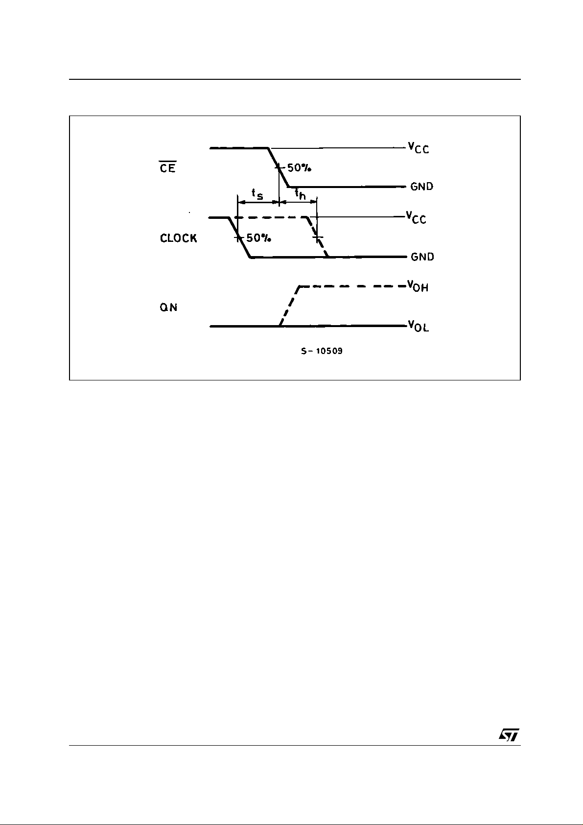
WAVEFORM 2 : MINIMUM SETUP AND HOLD TIME (f=1MHz; 50% duty cycle)
M74HC4017
WAVEFORM 3 : MINIMUM PULSE WIDTH, PROPAGATION DELAY (f=1MHz; 50% duty cycle)
7/12
M74HC4017
WAVEFORM 4 : MINIMUM SETUP AND HOLD TIME(f=1MHz; 50% duty cycle)
8/12

M74HC4017
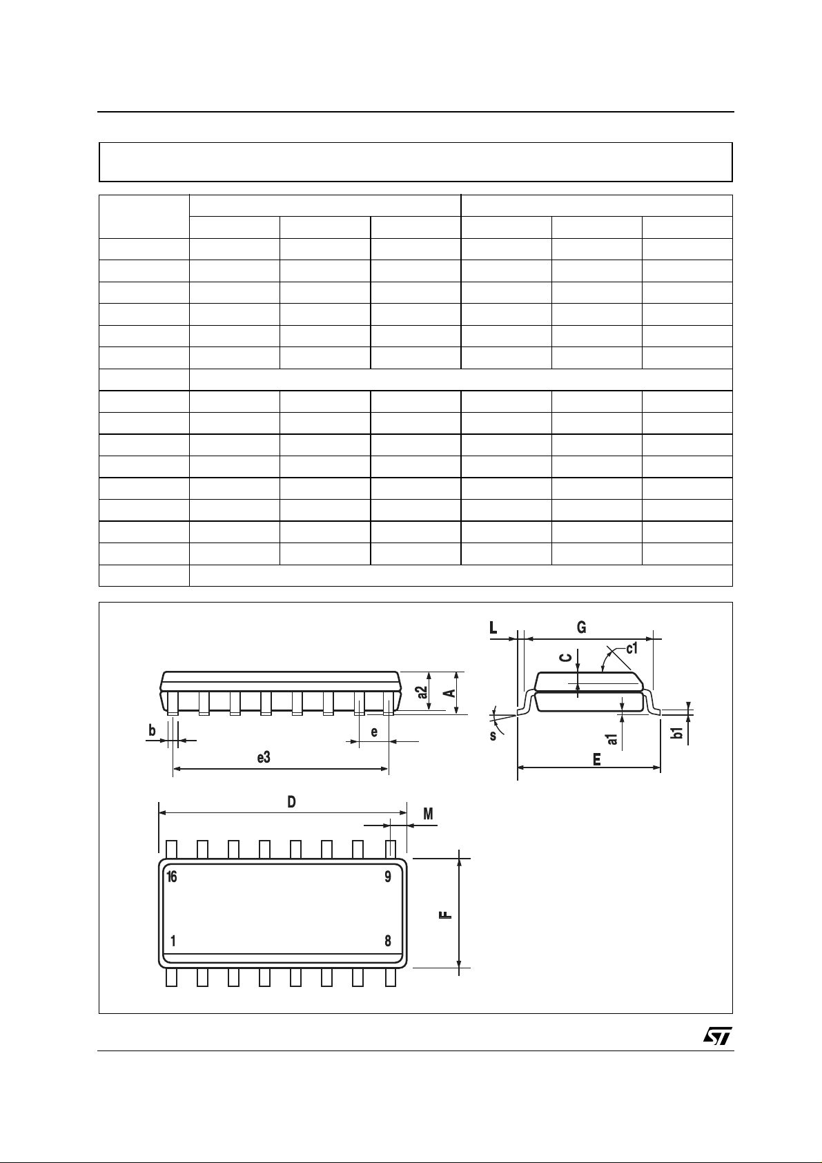
Plastic DIP-16 (0.25) MECHANICAL DATA
mm. inch
DIM.
MIN. TYP MAX. MIN. TYP. MAX.
a1 0.51 0.020
B 0.77 1.65 0.030 0.065
b 0.5 0.020
b1 0.25 0.010
D 20 0.787
E 8.5 0.335
e 2.54 0.100
e3 17.78 0.700
F 7.1 0.280
I 5.1 0.201
L 3.3 0.130
Z 1.27 0.050
P001C
9/12
M74HC4017
SO-16 MECHANICAL DATA
DIM.
A 1.75 0.068
a1 0.1 0.2 0.003 0.007
a2 1.65 0.064
b 0.35 0.46 0.013 0.018
b1 0.19 0.25 0.007 0.010
C 0.5 0.019
c1 45° (typ.)
D 9.8 10 0.385 0.393
E 5.8 6.2 0.228 0.244
e 1.27 0.050
e3 8.89 0.350
F 3.8 4.0 0.149 0.157
G 4.6 5.3 0.181 0.208
L 0.5 1.27 0.019 0.050
M 0.62 0.024
S8° (max.)
MIN. TYP MAX. MIN. TYP. MAX.
mm. inch
10/12
PO13H

M74HC4017
TSSOP16 MECHANICAL DATA
mm. inch
DIM.
MIN. TYP MAX. MIN. TYP. MAX.
A 1.2 0.047
A1 0.05 0.15 0.002 0.004 0.006
A2 0.8 1 1.05 0.031 0.039 0.041
b 0.19 0.30 0.007 0.012
c 0.09 0.20 0.004 0.0089
D 4.9 5 5.1 0.193 0.197 0.201
E 6.2 6.4 6.6 0.244 0.252 0.260
E1 4.3 4.4 4.48 0.169 0.173 0.176
e 0.65 BSC 0.0256 BSC
K0° 8°0° 8°
L 0.45 0.60 0.75 0.018 0.024 0.030
A2
A
A1
b
e
c
K
L
E
D
E1
PIN 1 IDENTIFICATION
1
0080338D
11/12

M74HC4017
Information furnished is bel ieved to be accurate and reliable. However, STMicroe lectronics assumes no responsibility for the
consequences of use of such information nor for any infringement of patents or other rights of third parties which may result from
its use. No li cense is granted by i mp lication or otherwise under a ny patent or patent rig h ts of S TMic roelec tronics. Specifications
mentioned in this publication ar e subject to change without notice. This publication supersedes and replaces all information
previously supplied. S TMicroelectronics products are not authorized for use as critica l components in life suppo rt devices or
systems without express written approval of STMicroelectronics.
Australi a - Brazil - Chi na - Finlan d - F rance - Germ any - Hong Kon g - India - Italy - Japan - Ma l aysia - Malta - Morocco
© The ST logo is a registered trademark of STMicroelectronics
© 2001 STM icroelectronics - P rinted in Italy - All Righ ts Reserved
STMicr o el ectronics GROUP OF COMPA NI E S
Singapo re - Spain - Sweden - Swit zerland - Un i ted Kingdom
© http://www.st.com
12/12
 Loading...