

ST M74HC4016 User Manual
M74HC4016
Obsolete Product(s) - Obsolete Product(s) Obsolete Product(s) - Obsolete Product(s)
QUAD BILATERAL SWITCH
■ HIGH SPEED:
t
= 9ns (TYP.) at VCC = 6V
PD
■ LOW POWER DISSIPATION:
I
= 1µA(MAX.) at TA=25°C
CC
■ LOW "ON" RESISTANCE:
R
= 60Ω TYP. AT VCC = 9V, I
ON
■ WIDE OPERATING VOLTAGE RANGE
V
(OPR) = 2V TO 12V
CC
■ SINE WAVE DISTORTION:
0.042% at V
■ HIGH NOISE IMMUNITY:
V
= V
NIH
■ PIN AND FUNCTION COMPATIBLE WITH
= 9Vpp , f = 1KHz
CC
= 28 % VCC (MIN.)
NIL
= 100 µA
I/O
74 SERIES 4016
DESCRIPTION
The M74HC4016 is an high speed CMOS QUAD
BILATERAL SW ITCH fabricated with silicon gate
2
C
MOS technology.
TSSOPDIP SOP
ORDER CODES
PACKAGE TUBE T & R
DIP M74HC4016B1R
SOP M74HC4016M1R M74HC4016RM13TR
TSSOP M74HC4016TTR
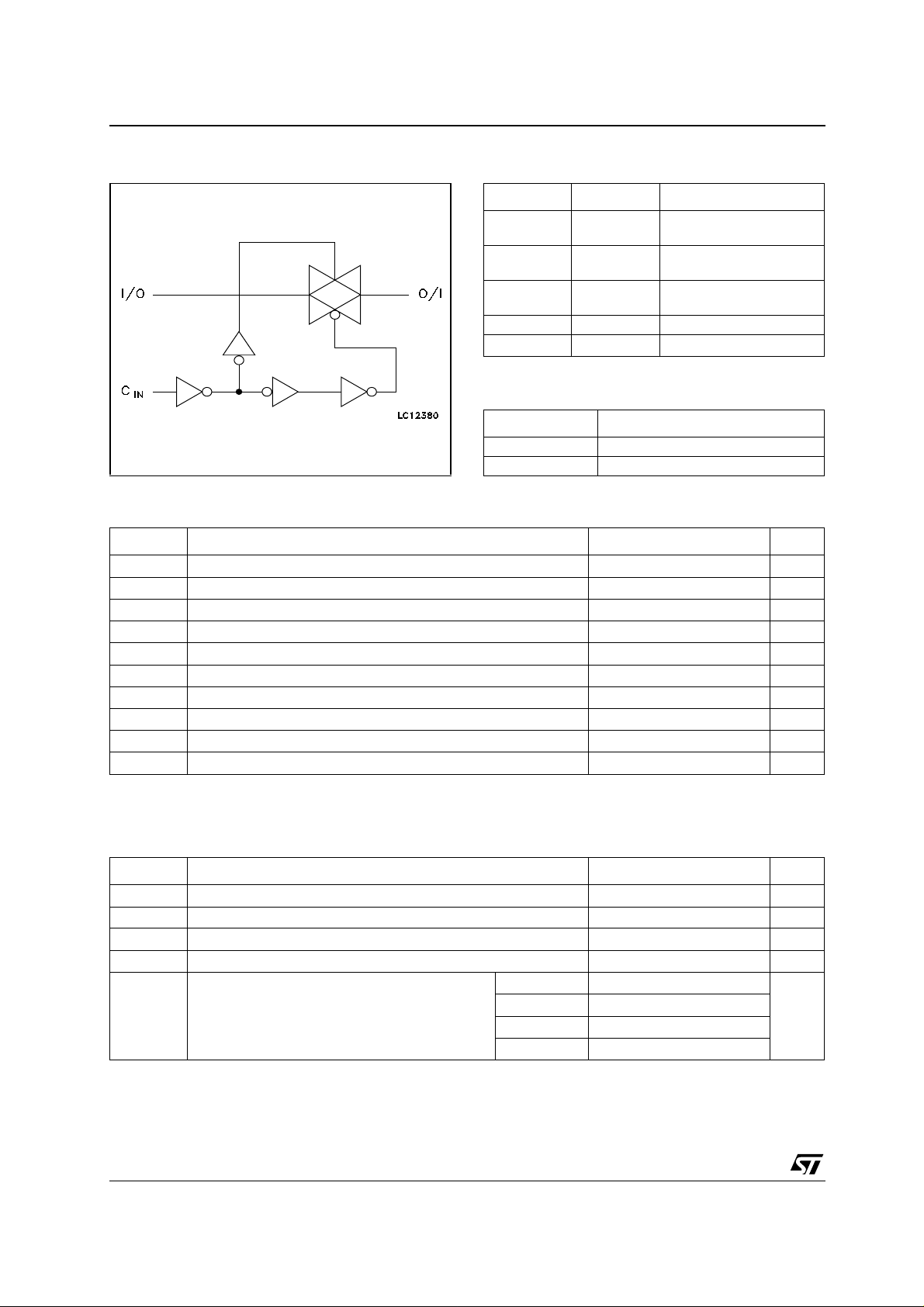
The C input is provided to control the switch; the
switch is on when the C input is held high and off
when C is held low.
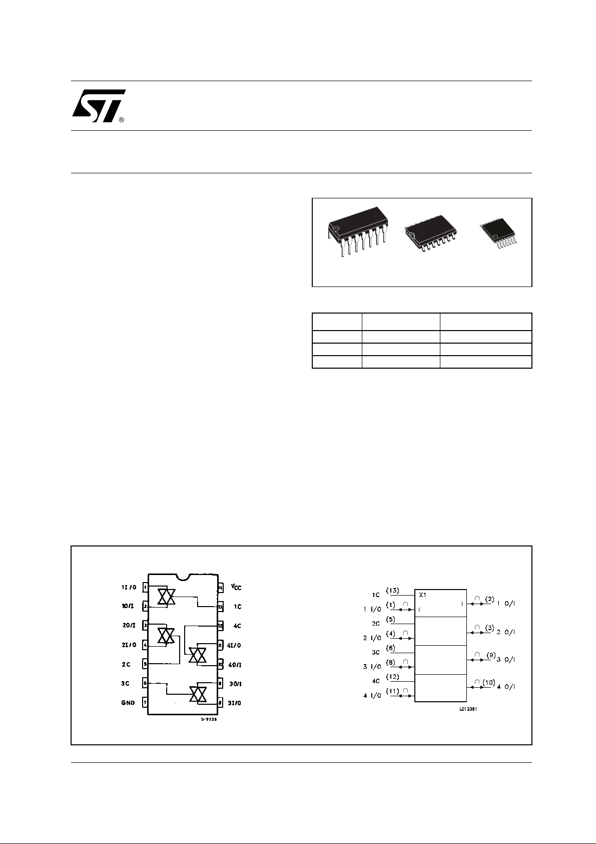
PIN CONNECTION AND IEC LOGIC SYM BOLS
1/11August 2001
Obsolete Product(s) - Obsolete Product(s) Obsolete Product(s) - Obsolete Product(s)
M74HC4016
LOGIC DIAGRAM PIN DESCRIPTION
PIN No SYMBOL NAME AND FUNCTION
1, 4, 8, 11 1 to 4 I/O Independent Inputs/Out-
2, 3, 9, 10 1 to 4 O/I Independent Outputs/
13, 5, 6, 12 1C to 4C Enable Inputs (Active
7 GND Ground (0V)
14 V
CC
TRUTH TABLE
CONTROL SWITCH FUNCTION
HON
LOFF
ABSOLUTE MAXIMUM RATINGS
Symbol Parameter Value Unit
V
V
V
I
OK
I
IOK
I
I
or I
CC
P
T
T
Absolute Maximum Ratings are those values beyond which damage to the device may occur. Functional operation under these conditions is
not implied
(*) 500mW at 65
Supply Voltage
CC
DC Input Voltage -0.5 to VCC + 0.5
IN
DC Input/Output Voltage -0.5 to VCC + 0.5
I/O
Control Input DC Diode Current
I/O DC Diode Current
DC Output Source Sink Current Per Output Pin
O
DC VCC or Ground Current
GND
Power Dissipation
D
Storage Temperature
stg
Lead Temperature (10 sec)
L
°C; derate to 300mW by 10mW/°C from 65°C to 85°C
puts
Inputs
High)
Positive Supply Voltage
-0.5 to +13 V
V
V
± 20 mA
± 20 mA
± 25 mA
± 50 mA
500(*) mW
-65 to +150 °C
300 °C
RECOMMENDED OPERATING CONDITIONS
Symbol Parameter Value Unit
V
V
V
T
t
r
2/11
Supply Voltage
CC
Input Voltage (Control) 0 to V
IN
I/O Voltage 0 to V
I/O
Operating Temperature
op
Input Rise and Fall Time VCC = 2.0V
V
= 4.5V
, t
f
CC
V
CC
V
CC
= 6.0V
= 10.0V
2 to 12 V
CC
CC
-55 to 125 °C
0 to 1000
0 to 500
0 to 400
ns
0 to 250
V
V
Obsolete Product(s) - Obsolete Product(s) Obsolete Product(s) - Obsolete Product(s)
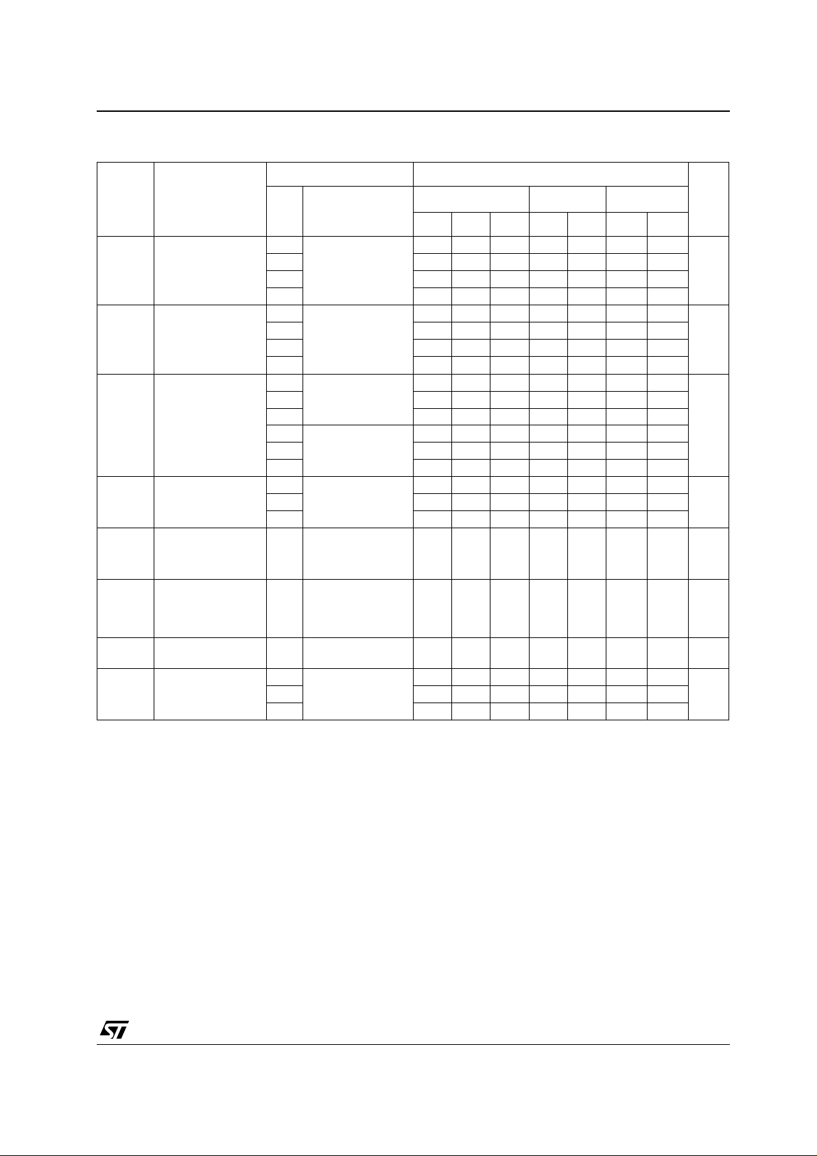
DC SPECIFICATIONS
Symbol Parameter
V
V
R
∆R
I
High Level Control
IHC
Input Voltage
Low Level Control
ILC
Input Voltage
ON Resistance 4.5 VIN = V
ON
Difference of ON
ON
Resistance
between switches
Input/Output
OFF
Leakage Current
(SWITCH OFF)
I
Switch Input
IZ
Leakage Current
(SWITCH ON,
OUTPUT OPEN)
I
Control Input
IN
Current
I
Quiescent Supply
CC
Current
M74HC4016
Test Condition Value
T
= 25°C
V
CC
(V)
A
Min. Typ. Max. Min. Max. Min. Max.
2.0 1.5 1.5 1 .5
4.5 3.15 3.15 3.15
9.0 6.3 6.3 6 .3
12.0 8.4 8.4 8 .4
2.0 0.5 0.5 0.5
4.5 1.35 1.35 1.35
9.0 2.5 2.5 2.5
12.0 3.6 3.6 3.6
V
9.0 85 170 213 260
I/O
12.0 60 120 150 180
I
4.5
V
9.0 60 120 150 200
I/O
12.0 50 100 125 150
I
4.5
V
I/O
12.0 6
I
IHC
= VCC to GND
= 100µA
I/O
= V
V
IN
IHC
= VCC or GND
= 100µA
I/O
= V
V
IN
IHC
= VCC or GND
≤ 100µA
I/O
160 320 400 450
80 160 200 250
16
VOS = VCC or GND
V
12.0
12.0
6.0
= VCC or GND
IS
V
= V
IN
= VCC or GND
V
OS
V
= V
IN
V
= VCC or GND
IN
ILC
IHC
6.0
V
= VCC or GND
IN
12.0 8 80 160
-40 to 85°C -55 to 125°C
± 0.1 ± 1 ± 2 µA
± 0.1 ± 1 ± 2 µA
± 0.1 ± 1 ± 1 µA
11020
Unit
V
V
Ω
Ω9.0 9
µA9.0 4 40 80
3/11
Obsolete Product(s) - Obsolete Product(s) Obsolete Product(s) - Obsolete Product(s)
M74HC4016
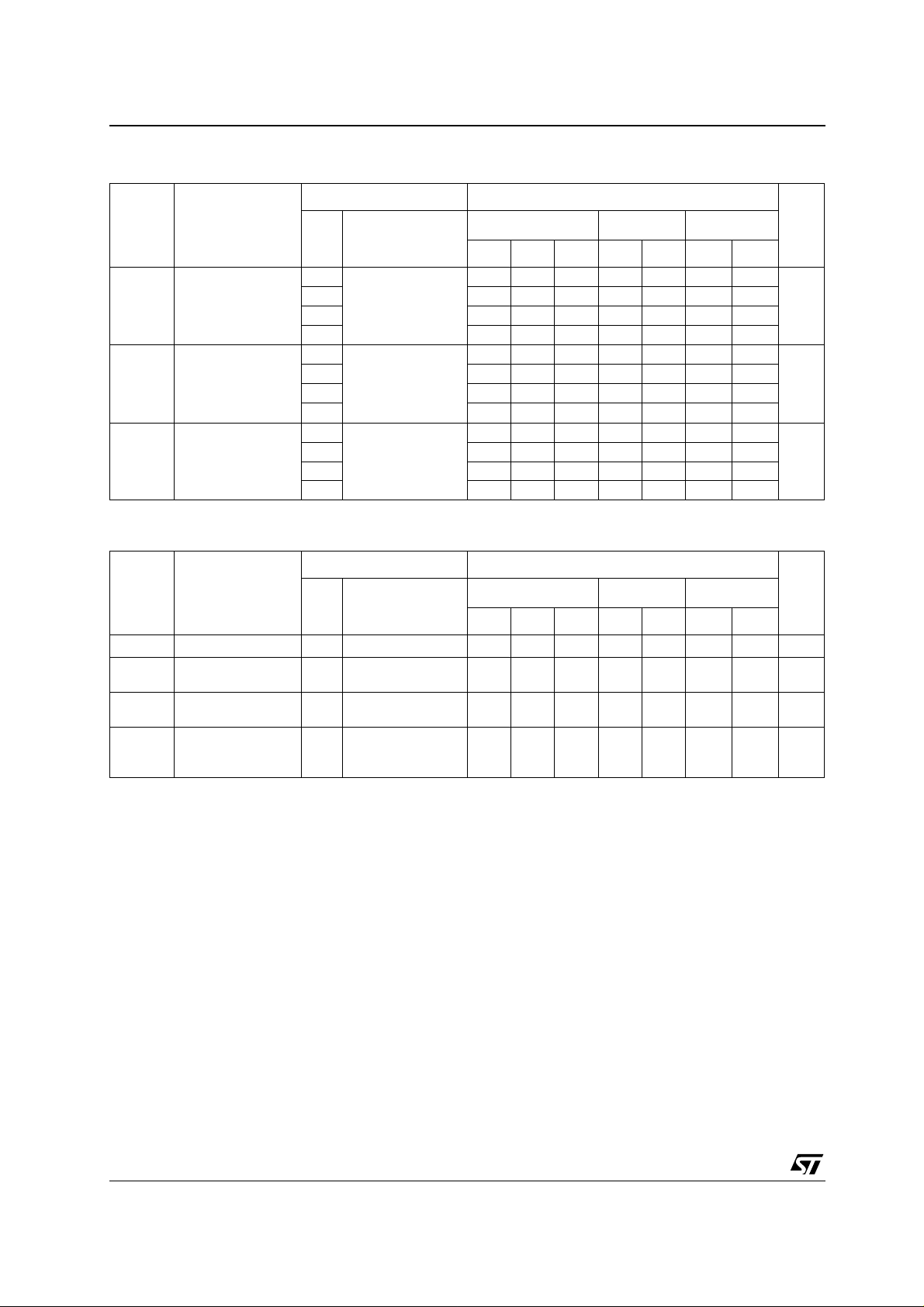
AC ELECTRICAL CHARACTERISTICS (CL = 50 pF, Input tr = tf = 6ns)
Test Condition Value
T
Symbol Parameter
V
CC
(V)
Φ
Phase Difference
I/O
Between Input and
Output
2.0 20 50 65 75
4.5 5 10 13 15
9.0 4 8 10 12
12.0 3 7 9 11
t
t
Output Enable Time 2.0
PZL
PZH
4.5 10 20 25 30
9.0 8 15 20 24
12.0 7 14 18 21
t
PLZ
t
PHZ
Output Disable
Time
2.0
4.5 15 30 38 45
9.0 10 26 33 36
12.0 8 24 30 32
CAPACITIVE CHARACTERISTICS
R
L
R
L
= 1KΩ
= 1KΩ
= 25°C
A
Min. Typ. Max. Min. Max. Min. Max.
40 100 125 150
60 150 190 225
-40 to 85°C -55 to 125°C
Unit
ns
ns
ns
Test Condition Value
Symbol Parameter
V
CC
(V)
C
Input Capacitanc e 5 10 10 1 0 pF
IN
C
C
C
Switch Terminal
I/O
Capacitance
Feed Through
IOS
Capacitanc e
Power Dissipation
PD
Capacitance
= 25°C
A
Min. Typ. Max. Min. Max. Min. Max.
5pF
1pF
15 pF
-40 to 85°C -55 to 125°C
Unit
T
(note 1)
1) CPD is defined as the value of the IC’s internal equivalent capacitance which is calculated from the operating current consumption without
load. (R ef er to Test Circ ui t). Averag e operatin g current can be obtained by t he following equation. I
= CPD x VCC x fIN + ICC
CC(opr)
4/11
 Loading...