


M74HC393
DUAL BINARY COUNTER
■ HIGH SPEED :
f
= 79 MHz (TYP.) at VCC = 6V
MAX
■ LOW POWER DISSIPATION:
I
=4µA(MAX.) at TA=25°C
CC
■ HIGH NOISE IMMUNITY:
V
= V
NIH
■ SYMMETRICAL OUTPUT IMPEDANCE:
|I
| = IOL = 4mA (MIN)
OH
■ BALANCED PROPAGATION DELAYS:
t
≅ t
PLH
■ WIDE OPERATING VOLTAGE RANGE:
V
(OPR) = 2V to 6V
CC
■ PIN AND FUNCTION COMPATIBLE WITH
= 28 % VCC (MIN.)
NIL
PHL
74 SERIES 393
DESCRIPTION
The M74HC393 is an high speed CMOS DUAL
BINARY COUNTER fabricated with silicon gate
2
MOS technology.
C
This counter circuit contains independent ripple
carry counters and two 4-bit ripple carry binary
counters, which can be cascaded to create a
single divide by 256 counter.
Each 4-bit counter is incremented on the high to
low transition (neg ative edge) of the clock inp ut,
TSSOPDIP SOP
ORDER CODES
PACKAGE TUBE T & R
DIP M74HC393B1R
SOP M74HC393M1R M74HC393RM13TR
TSSOP M74HC393TTR
and each has an indep endent clear input. When
CLEAR is set to low, all four bits of each count er
are set to a low level. This enables count
truncation and allows the implementation of divide
by N counter configurations.
All inputs are equipped with protection circuits
against static discharge and transient excess
voltage.
PIN CONNECTION AND IEC LOGIC SYMBOLS
1/11July 2001

M74HC393
INPUT AND OUTPUT EQUIVALENT CIRCUIT PIN DESCRIPTION
PIN No SYMBOL NAME AND FUNCTION
1, 13
2, 12
3, 4, 5, 6 1QA to 1QD Flip Flop Outputs
11, 10, 9, 8 2QA to 2QD Flip Flop Outputs
7 GND Ground (0V)
14 Vcc Positive Supply Voltage
TRUTH TABLE
INPUTS OUTPUTS
1 CLOCK
2 CLOCK
1 CLEAR
2 CLEAR
Clock Input Divide by 2
Section (HIGH to LOW
Edge-Triggered)
Asynchronous Master
Reset Inputs
CLOCK
XHLLLL
X : Don’t Ca r e
CLEAR QD QC QB QA
L COUNT UP
L NO CHANGE
OUTPUTS
COUNT
QD QC QB QA
0LLLL
1LLLH
2LLHL
3LLHH
4LHLL
5LHLH
6LHHL
7LHHH
8HLLL
9HLLH
10 HLHL
11 H L H H
12 H H L L
13 H H L H
14 H H H L
15 HHHH
2/11

LOGIC DIAGRAM
M74HC393
This log i c diagram has not be used to est i m at e propagation delays
TIMING CHART
3/11
M74HC393
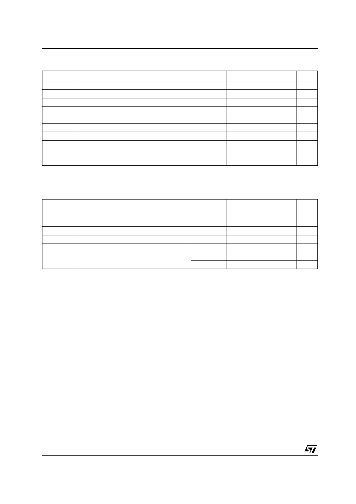
ABSOLUTE MAXIMUM RATINGS
Symbol Parameter Value Unit
V
V
V
I
I
OK
I
I
or I
CC
P
T
T
Absolute Maximum Ratings are those values beyond which damage to the device may occur. Functional operation under these conditions is
not implied
(*) 500mW at 65
RECOMMENDED OPERATING CONDITIONS
Symbol Parameter Value Unit
V
V
V
T
t
r
Supply Voltage
CC
DC Input Voltage -0.5 to VCC + 0.5
I
DC Output Voltage -0.5 to VCC + 0.5
O
DC Input Diode Current
IK
DC Output Diode Current
DC Output Current
O
DC VCC or Ground Current
GND
Power Dissipation
D
Storage Temperature
stg
Lead Temperature (10 sec)
L
°C; derate to 300mW by 10mW/°C from 65°C to 85°C
Supply Voltage
CC
Input Voltage 0 to V
I
Output Voltage 0 to V
O
Operating Temperature
op
Input Rise and Fall Time VCC = 2.0V
, t
f
V
V
CC
CC
= 4.5V
= 6.0V
-0.5 to +7 V
± 20 mA
± 20 mA
± 25 mA
± 50 mA
500(*) mW
-65 to +150 °C
300 °C
2 to 6 V
CC
CC
-55 to 125 °C
0 to 1000 ns
0 to 500 ns
0 to 400 ns
V
V
V
V
4/11
 Loading...