

ST M74HC377 User Manual
M74HC377
OCTAL D TYPE FLIP FL O P
■ HIGH SPEED :
f
= 66 MHz (TYP.) at VCC = 6V
MAX
■ LOW POWER DISSIPATION:
I
=4µA(MAX.) at TA=25°C
CC
■ HIGH NOISE IMMUNITY:
V
= V
NIH
■ SYMMETRICAL OUTPUT IMPEDANCE:
|I
| = IOL = 4mA (MIN)
OH
■ BALANCED PROPAGATION DELAYS:
t
≅ t
PLH
■ WIDE OPERATING VOLTAGE RANGE:
V
(OPR) = 2V to 6V
CC
■ PIN AND FUNCTION COMPATIBLE WITH
= 28 % VCC (MIN.)
NIL
PHL
74 SERIES 377
DESCRIPTION
The M74HC377 is an high speed CMOS OCTAL
D TYPE FLIP FLOP fabricated with silicon gate
2
MOS technology.
C
Information at the D inputs meeting the setup time
requirements is transferred to the Q outputs on the
positive going edge of the clock pulse if the enable
input G
is low. Clock triggering occurs at a
particular voltage level and is not directly related
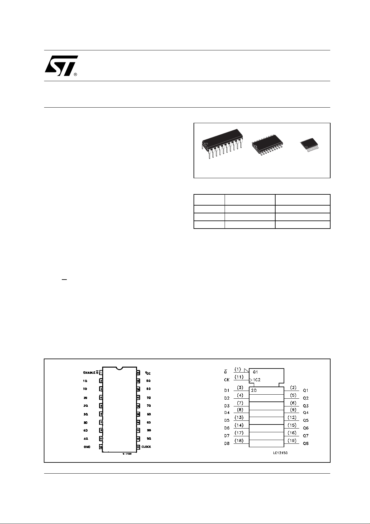
TSSOPDIP SOP
ORDER CODES
PACKAGE TUBE T & R
DIP M74HC377B1R
SOP M74HC377M1R M74HC377RM13TR
TSSOP M74HC377TTR
to the transition time of the positive going pulse.
When the clock input is at either the high or low
level, the D input signal has no effect at the output.
All inputs are equipped with protection circuits
against static discharge and transient excess
voltage.
PIN CONNECTION AND IEC LOGIC SYMBOLS
1/11July 2001
M74HC377
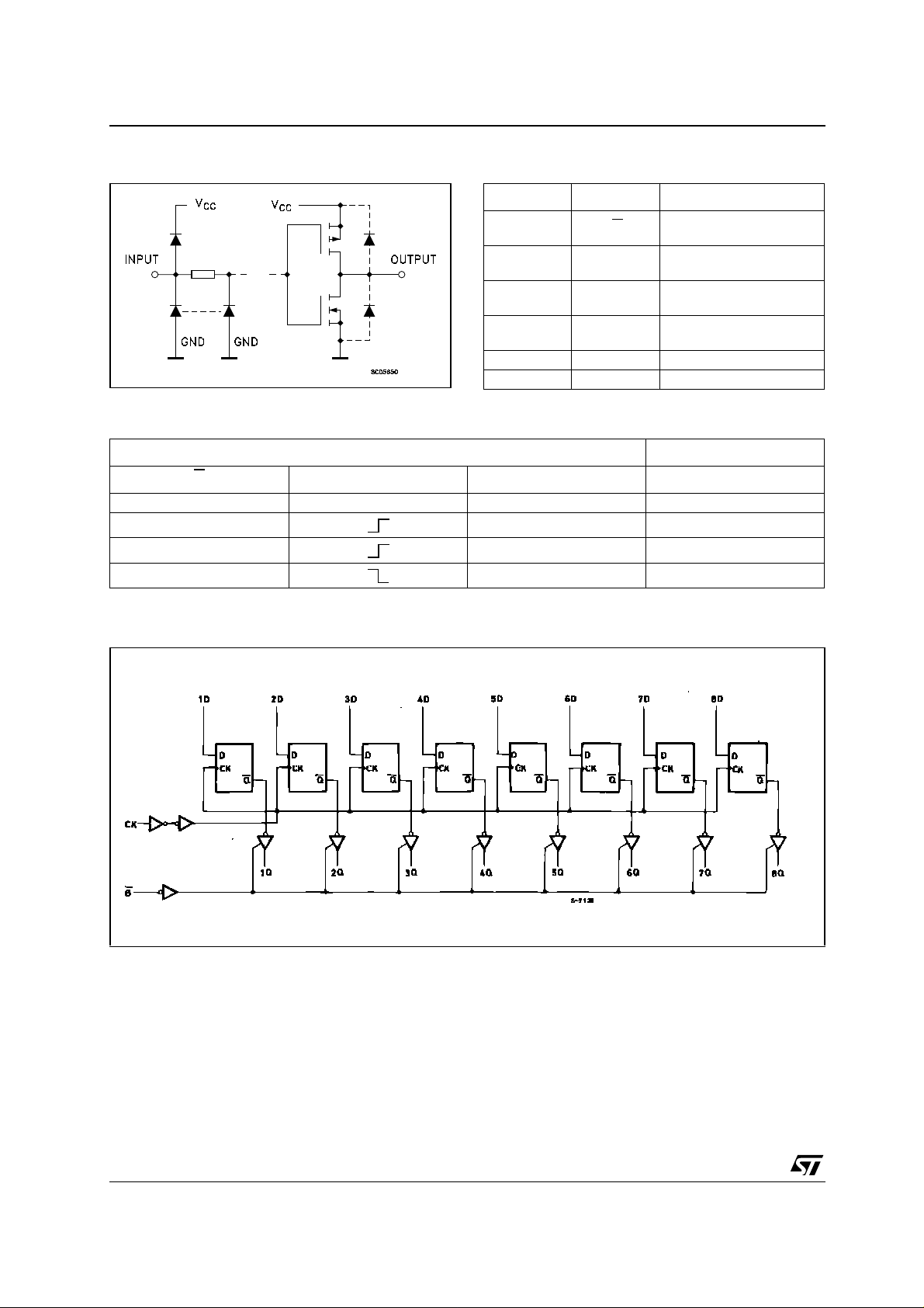
INPUT AND OUTPUT EQUIVALENT CIRCUIT PIN DESCRIPTION
PIN No SYMBOL NAME AND FUNCTION
1 G
2, 5, 6, 9, 12,
15, 16, 19
3, 4, 7, 8, 13,
14, 17, 18
11 CLOCK
10 GND Ground (0V)
20 Vcc Positive Supply Voltage
TRUTH TABLE
INPUTS OUTPUTS
1Q to 8Q Flip Flop Outputs
1D to 8D Data Inputs
Data Enable Input (Active
LOW)
Clock Input (LOW to
HIGH, Edge Triggered)
G
H X X NO CHANGE
LLL
LHH
X X NO CHANGE
X : Don’t Care
LOGIC DIAGRAM
CLOCK DATA Q
This log i c diagram has not be used to est i m at e propagation delays
2/11
M74HC377
ABSOLUTE MAXIMUM RATINGS
Symbol Parameter Value Unit
V
V
V
I
I
OK
I
I
or I
CC
P
T
T
Absolute Maximum Ratings are those values beyond which damage to the device may occur. Functional operation under these conditions is
not implied
(*) 500mW at 65
RECOMMENDED OPERATING CONDITIONS
Symbol Parameter Value Unit
V
V
V
T
t
r
Supply Voltage
CC
DC Input Voltage -0.5 to VCC + 0.5
I
DC Output Voltage -0.5 to VCC + 0.5
O
DC Input Diode Current
IK
DC Output Diode Current
DC Output Current
O
DC VCC or Ground Current
GND
Power Dissipation
D
Storage Temperature
stg
Lead Temperature (10 sec)
L
°C; derate to 300mW by 10mW/°C from 65°C to 85°C
Supply Voltage
CC
Input Voltage 0 to V
I
Output Voltage 0 to V
O
Operating Temperature
op
Input Rise and Fall Time VCC = 2.0V
, t
f
V
V
CC
CC
= 4.5V
= 6.0V
-0.5 to +7 V
± 20 mA
± 20 mA
± 25 mA
± 50 mA
500(*) mW
-65 to +150 °C
300 °C
2 to 6 V
CC
CC
-55 to 125 °C
0 to 1000 ns
0 to 500 ns
0 to 400 ns
V
V
V
V
3/11
M74HC377
DC SPECIFICATIONS
Symbol Parameter
V
V
V
V
I
High Level Input
IH
Voltage
Low Level Input
IL
Voltage
High Level Output
OH
Voltage
Low Level Output
OL
Voltage
I
Input Leakage
I
Current
Quiescent Supply
CC
Current
Test Condition Value
V
(V)
CC
= 25°C
A
Min. Typ. Max. Min. Max. Min. Max.
-40 to 85°C -55 to 125°C
T
2.0 1.5 1.5 1.5
6.0 4.2 4.2 4.2
2.0 0.5 0.5 0.5
6.0 1.8 1.8 1.8
2.0
4.5
6.0
4.5
6.0
2.0
4.5
6.0
4.5
6.0
6.0
6.0
IO=-20 µA
I
=-20 µA
O
I
=-20 µA
O
I
=-4.0 mA
O
I
=-5.2 mA
O
IO=20 µA
I
=20 µA
O
I
=20 µA
O
I
=4.0 mA
O
I
=5.2 mA
O
= VCC or GND
V
I
= VCC or GND
V
I
1.9 2.0 1.9 1.9
4.4 4.5 4.4 4.4
5.9 6.0 5.9 5.9
4.18 4.31 4.13 4.10
5.68 5.8 5.63 5.60
0.0 0.1 0.1 0.1
0.0 0.1 0.1 0.1
0.0 0.1 0.1 0.1
0.17 0.26 0.33 0.40
0.18 0.26 0.33 0.40
± 0.1 ± 1 ± 1 µA
44080µA
Unit
V4.5 3.15 3.15 3.15
V4.5 1.35 1.35 1.35
V
V
4/11
 Loading...