

ST M74HC373 User Manual
M74HC373
OCTAL D-TYPE LATCH
WITH 3 STATE OUTPUT NON INVERTING
■ HIGH SPEED:
t
= 12ns (TYP.) at VCC = 6V
PD
■ LOW POWER DISSIPATION:
I
= 4µA(MAX.) at TA=25°C
CC
■ HIGH NOISE IMMUNITY:
= V
V
NIH
■ SYMMETRICAL OUTPUT IMPEDANCE:
|I
| = IOL = 6mA (MIN)
OH
■ BALANCED PROPAGATION DELAYS:
t
≅ t
PLH
■ WIDE OPERATING VOLTAGE RANGE:
V
(OPR) = 2V to 6V
CC
■ PIN AND FUNCTION COMPATIBLE WITH
= 28 % VCC (MIN.)
NIL
PHL
74 SERIES 373
DESCRIPTION
The M74HC373 is an high speed CMOS OCTAL
LATCH WITH 3-STATE OUTPUTS fabricated
with sub-micron silicon gate C
2
MOS technology.
This 8-BIT D-Type la tches is controlled by a latch
enable input (LE) and output enable input (OE
).
While the LE in put is held at a high level, the Q
outputs will follow the data input. When the LE is
taken low, the Q outputs will be latched at the logic
level of D input data.
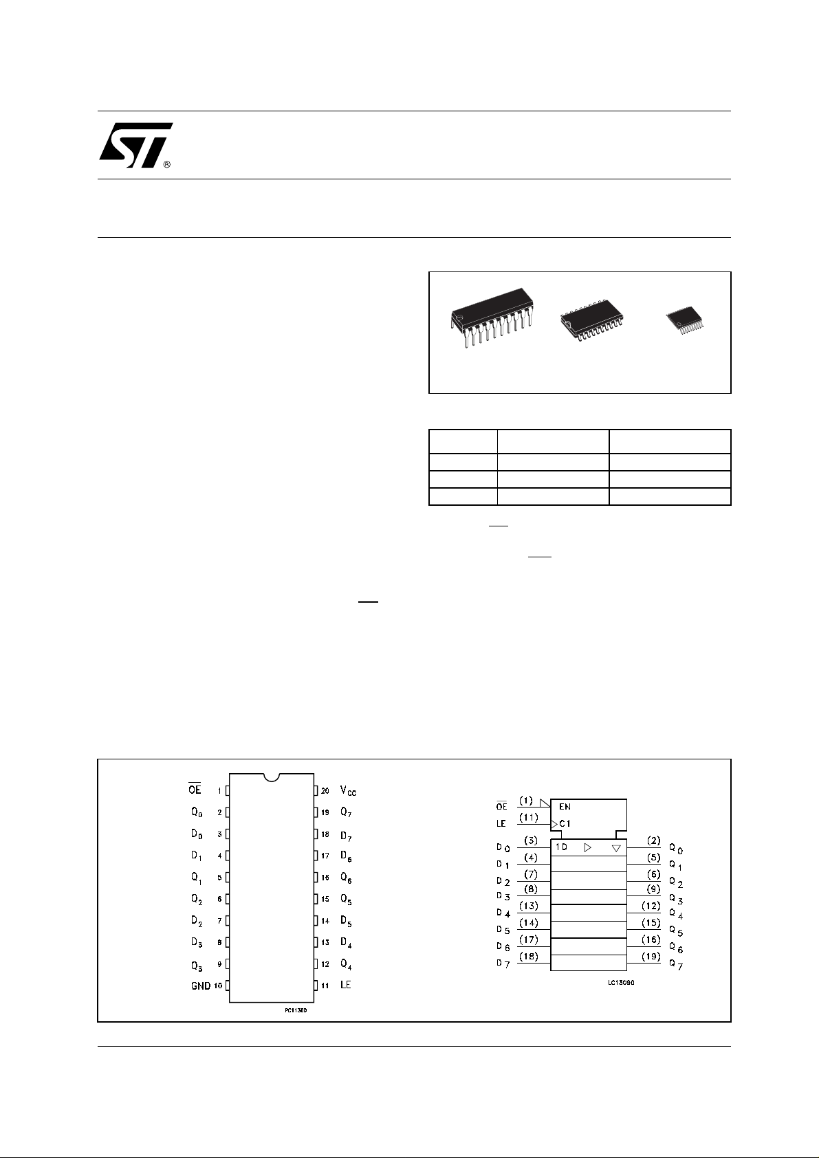
TSSOPDIP SOP
ORDER CODES
PACKAGE TUBE T & R
DIP M74HC373B1R
SOP M74HC373M1R M74HC373RM13TR
TSSOP M74HC373TTR
While the OE
input is at low level, the eight outputs
will be in a norm al logic state (high or low logic
level) and when OE
is in high level the outputs will
be in a high impedance state.
The 3-State output configuration and the wide
choice of outline make bus organized system
simple.
All inputs are equipped with protection circuits
against static discharge and transient excess
voltage.
PIN CONNECTION AND IEC LOGIC SYMBOLS
1/11July 2001
M74HC373
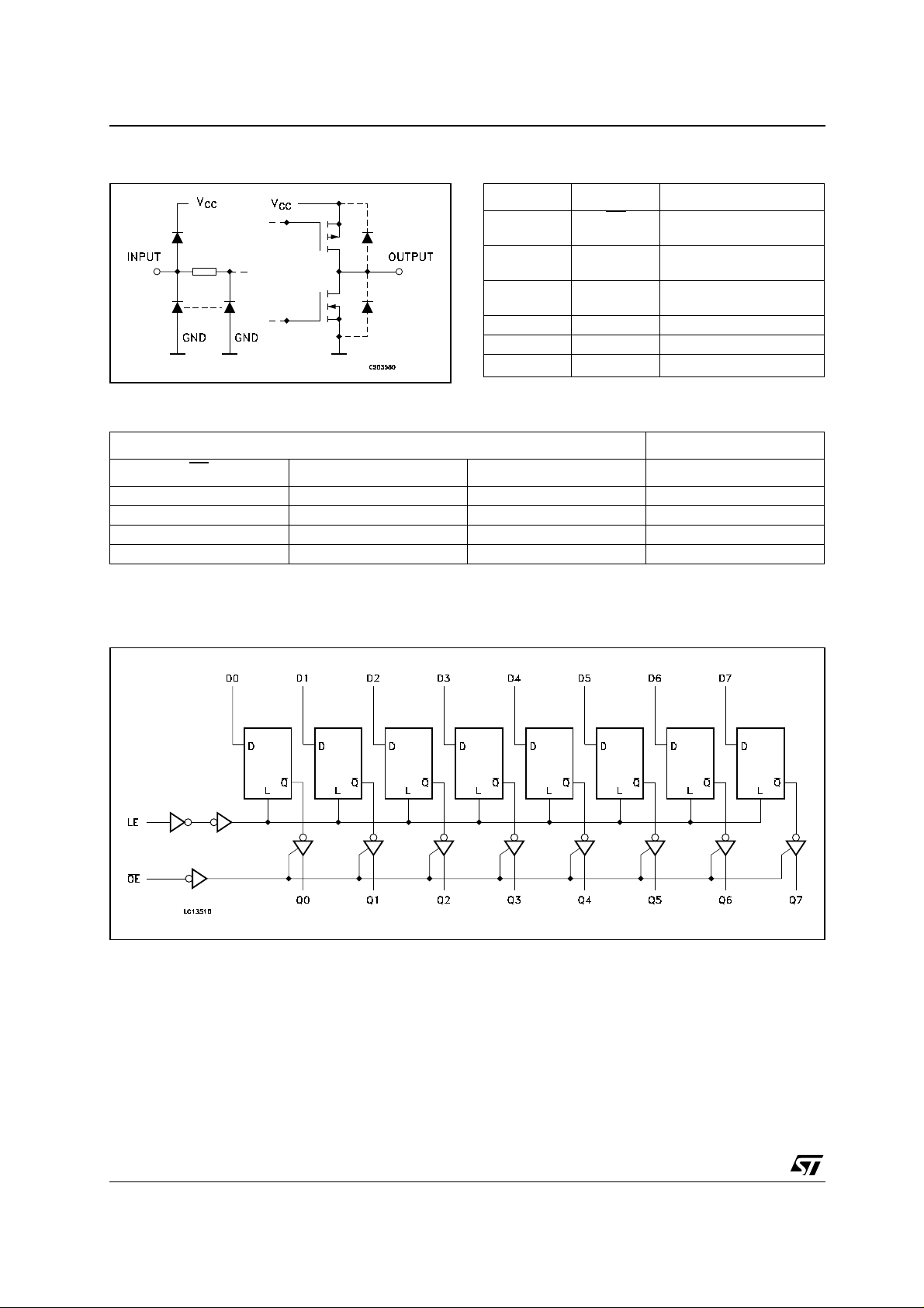
INPUT AND OUTPUT EQUIVALENT CIRCUIT PIN DESCRIPTION
PIN No SYMBOL NAME AND FUNCTION
1OE
2, 5, 6, 9, 12,
15, 16, 19
3, 4, 7, 8, 13,
14, 17, 18
11 LE Latch Enable Input
10 GND Ground (0V)
20 V
TRUTH TABLE
INPUTS OUTPUTS
Q0 to Q7 3 State Outputs
D0 to D7 Data Inputs
CC
3 State Output Enable
Input (Active LOW)
Positive Supply Voltage
OE
HXXZ
L L X NO CHANGE (*)
LHLL
LHHH
X: Don’t Care
Z: High Impedance
(*): Q Outputs are latched at the time when the LE inpu t is taken low logic level.
LE D Q
LOGIC DIAGRAM
2/11
M74HC373
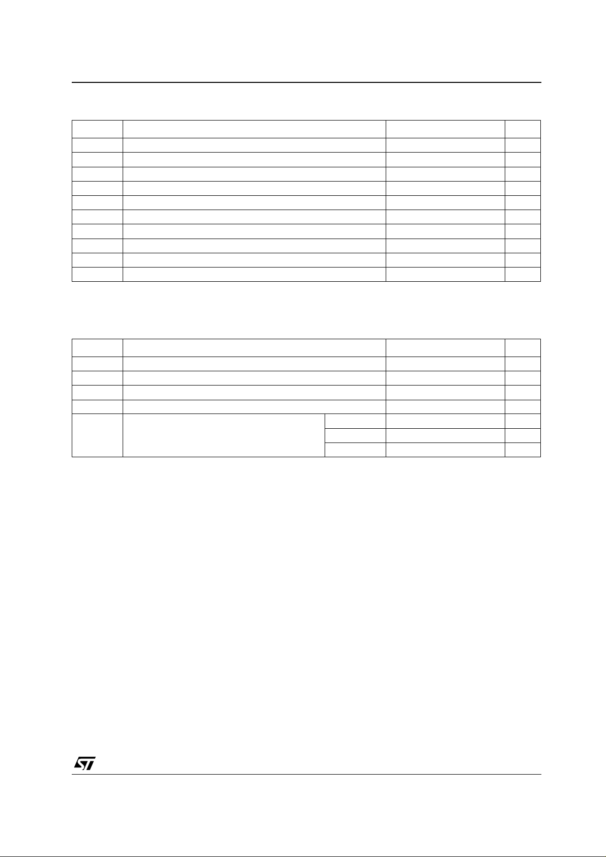
ABSOLUTE MAXIMUM RATINGS
Symbol Parameter Value Unit
V
V
V
I
I
OK
I
I
or I
CC
P
T
T
Absolute Maximum Ratings are those values beyond which damage to the device may occur. Functional operation under these conditions is
not implied
(*) 500mW at 65
RECOMMENDED OPERATING CONDITIONS
Symbol Parameter Value Unit
V
V
V
T
t
r
Supply Voltage
CC
DC Input Voltage -0.5 to VCC + 0.5
I
DC Output Voltage -0.5 to VCC + 0.5
O
DC Input Diode Current
IK
DC Output Diode Current
DC Output Current
O
DC VCC or Ground Current
GND
Power Dissipation
D
Storage Temperature
stg
Lead Temperature (10 sec)
L
°C; derate to 300mW by 10mW/°C from 65°C to 85°C
Supply Voltage
CC
Input Voltage 0 to V
I
Output Voltage 0 to V
O
Operating Temperature
op
Input Rise and Fall Time VCC = 2.0V
, t
f
V
V
CC
CC
= 4.5V
= 6.0V
-0.5 to +7 V
± 20 mA
± 20 mA
± 35 mA
± 70 mA
500(*) mW
-65 to +150 °C
300 °C
2 to 6 V
CC
CC
-55 to 125 °C
0 to 1000 ns
0 to 500 ns
0 to 400 ns
V
V
V
V
3/11
M74HC373
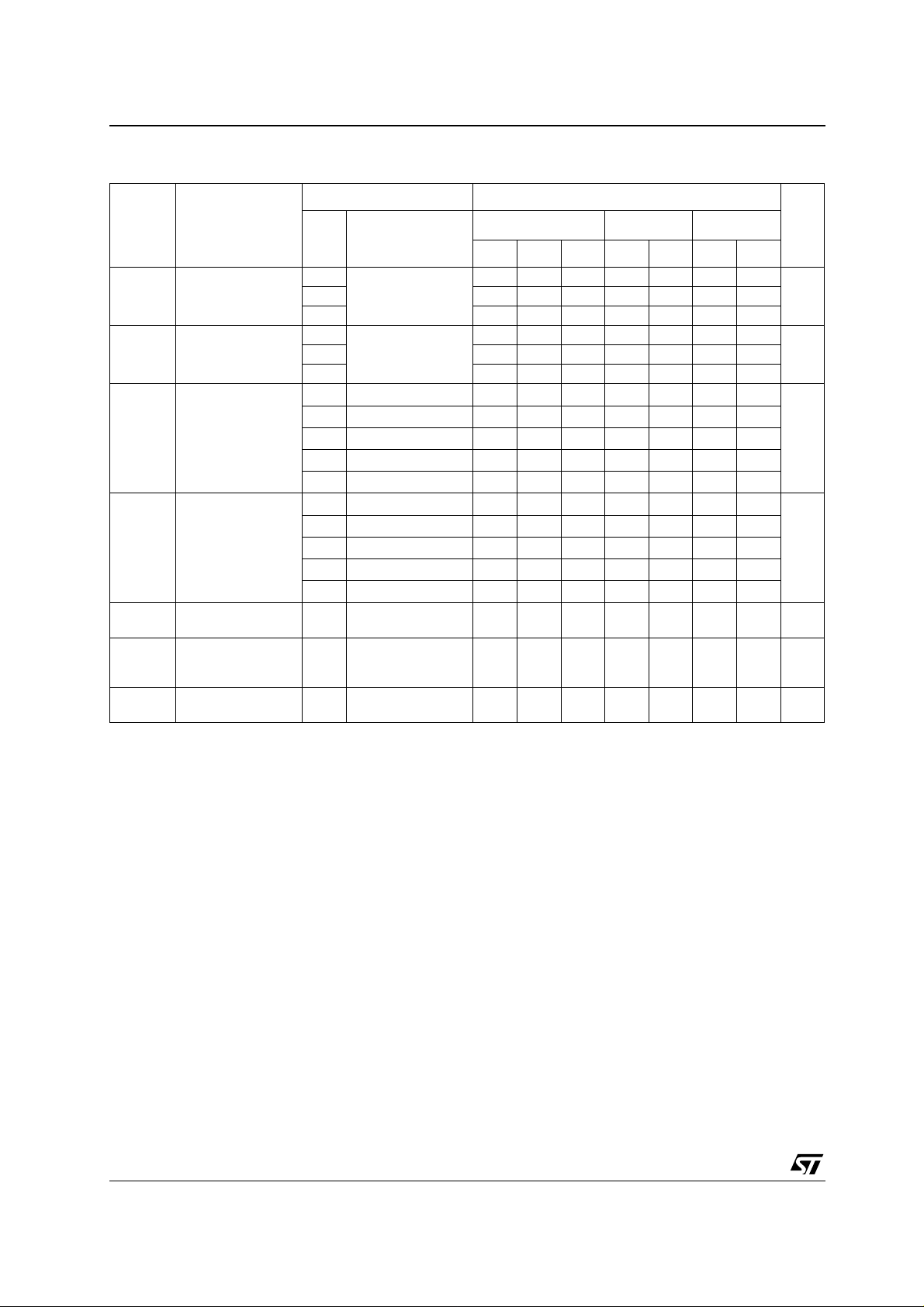
DC SPECIFICATIONS
Symbol Parameter
V
V
V
V
I
I
High Level Input
IH
Voltage
Low Level Input
IL
Voltage
High Level Output
OH
Voltage
Low Level Output
OL
Voltage
I
Input Leakage
I
Current
High Impedance
OZ
Output Leakage
Current
Quiescent Supply
CC
Current
Test Condition Value
V
CC
(V)
= 25°C
A
Min. Typ. Max. Min. Max. Min. Max.
-40 to 85°C -55 to 125°C
T
2.0 1.5 1.5 1.5
6.0 4.2 4.2 4.2
2.0 0.5 0.5 0.5
6.0 1.8 1.8 1.8
2.0
4.5
6.0
4.5
6.0
2.0
4.5
6.0
4.5
6.0
6.0
6.0
6.0
IO=-20 µA
I
=-20 µA
O
I
=-20 µA
O
I
=-6.0 mA
O
I
=-7.8 mA
O
IO=20 µA
I
=20 µA
O
I
=20 µA
O
I
=6.0 mA
O
I
=7.8 mA
O
= VCC or GND
V
I
= VIH or V
V
I
IL
VO = VCC or GND
= VCC or GND
V
I
1.9 2.0 1.9 1.9
4.4 4.5 4.4 4.4
5.9 6.0 5.9 5.9
4.18 4.31 4.13 4.10
5.68 5.8 5.63 5.60
0.0 0.1 0.1 0.1
0.0 0.1 0.1 0.1
0.0 0.1 0.1 0.1
0.17 0.26 0.33 0.40
0.18 0.26 0.33 0.40
± 0.1 ± 1 ± 1 µA
± 0.5 ± 5 ± 10 µA
44080µA
Unit
V4.5 3.15 3.15 3.15
V4.5 1.35 1.35 1.35
V
V
4/11
 Loading...