

ST M74HC27 User Manual
M74HC27
TRIPLE 3-INPUT NOR GATE
■ HIGH SPEED:
t
= 9ns (TYP.) at VCC = 6V
PD
■ LOW POWER DISSIPATION:
I
= 1µA(MAX.) at TA=25°C
CC
■ HIGH NOISE IMMUNITY:
V
= V
NIH
■ SYMMETRICAL OUTPUT IMPEDANCE:
|I
| = IOL = 4mA (MIN)
OH
■ BALANCED PROPAGATION DELAYS:
t
≅ t
PLH
■ WIDE OPERATING VOLTAGE RANGE:
V
(OPR) = 2V to 6V
CC
■ PIN AND FUNCTION COMPATIBLE WITH
= 28 % VCC (MIN.)
NIL
PHL
74 SERIES 27
DESCRIPTION
The M74HC27 is an high speed CMOS TRIPLE
3-INPUT NOR GATE fabricated with si licon gate
2
MOS technology.
C
The internal circuit is composed of 3 stages
including buffer output , which enables high noise
immunity and stable output.
TSSOPDIP SOP
ORDER CODES
PACKAGE TUBE T & R
DIP M74HC27B1R
SOP M74HC27M1R M74HC27RM13TR
TSSOP M74HC27TTR
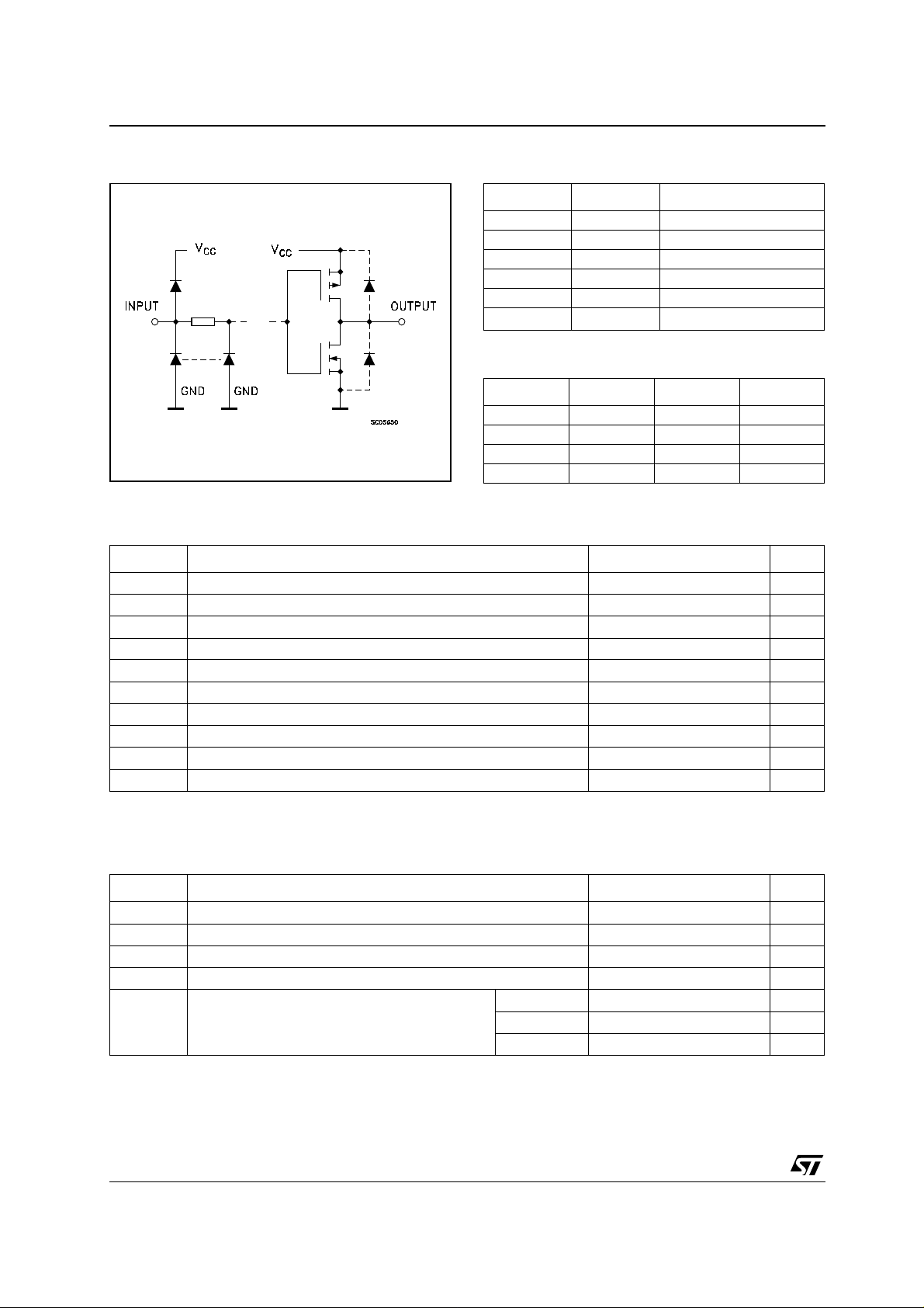
All inputs are equipped with protection circuits
against static discharge and transient excess
voltage.
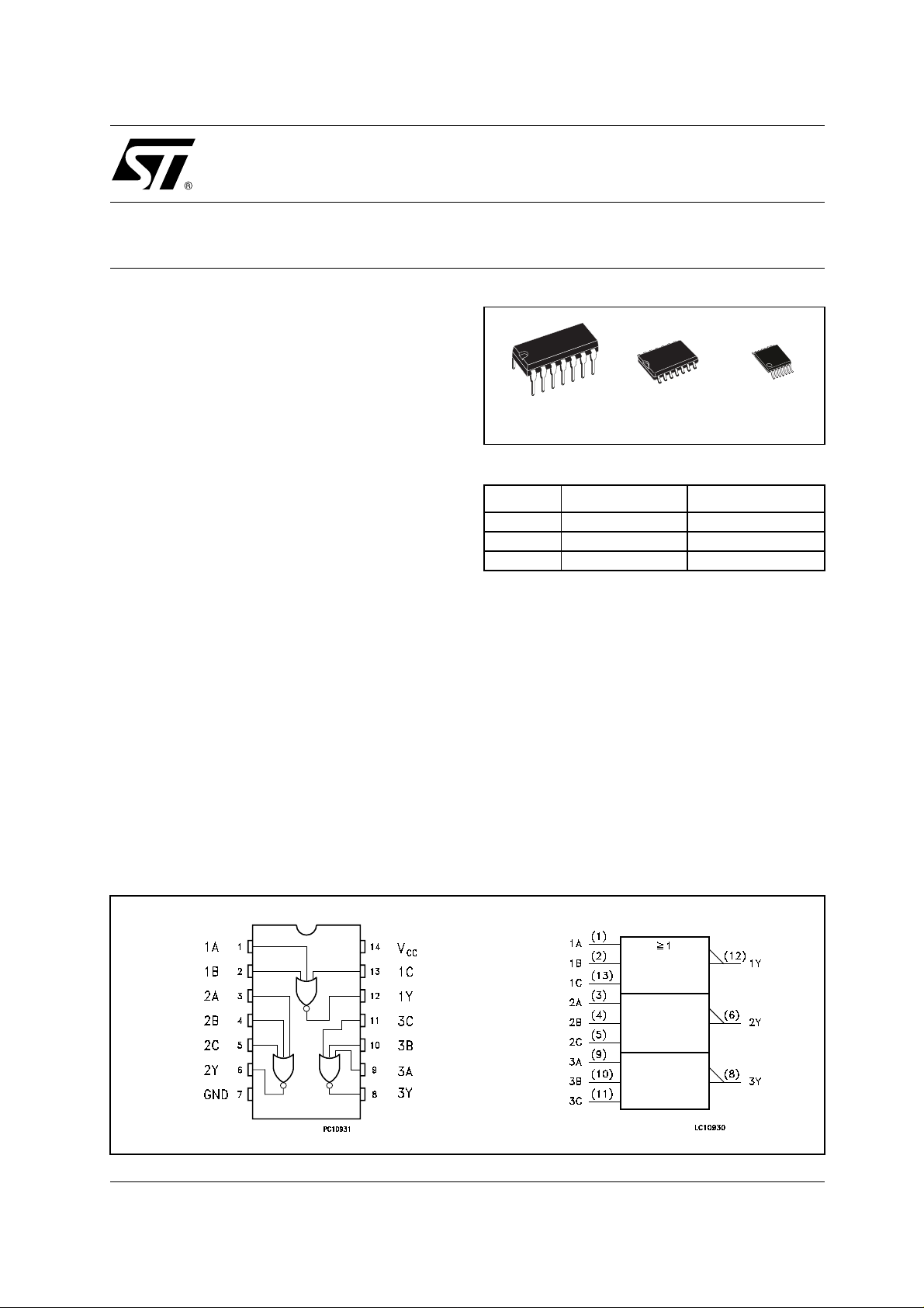
PIN CONNECTION AND IEC LOGIC SYMBOLS
1/8July 2001
M74HC27
INPUT AND OUTPUT EQUIVALENT CIRCUIT PIN DESCRIPTION
PIN No SYMBOL NAME AND FUNCTION
1, 3, 9 1A to 3A Data Inputs
2, 4, 10 1B to 3B Data Inputs
13, 5, 11 1C to 3C Data Inputs
12, 6, 8 1Y to 3Y Data Outputs
7 GND Ground (0V)
14
V
CC
TRUTH TABLE
ABCY
LLLH
HXXL
XHXL
XXHL
X : Don’t Care
ABSOLUTE MAXIMUM RATINGS
Symbol Parameter Value Unit
V
V
V
I
I
OK
I
I
or I
CC
P
T
T
Absolute Maximum Ratings are those values beyond which damage to the device may occur. Functional operation under these conditions is
not implied
(*) 500mW at 65
Supply Voltage
CC
DC Input Voltage -0.5 to VCC + 0.5
I
DC Output Voltage -0.5 to VCC + 0.5
O
DC Input Diode Current
IK
DC Output Diode Current
DC Output Current
O
DC VCC or Ground Current
GND
Power Dissipation
D
Storage Temperature
stg
Lead Temperature (10 sec)
L
; derate to 30 0m W by 10mW/°C from 65
°C
°C to 85°C
Positive Supply Voltage
-0.5 to +7 V
V
V
± 20 mA
± 20 mA
± 25 mA
± 50 mA
500(*) mW
-65 to +150 °C
300 °C
RECOMMENDED OPERATING CONDITIONS
Symbol Parameter Value Unit
2/8
V
V
V
T
t
r
Supply Voltage
CC
Input Voltage 0 to V
I
Output Voltage 0 to V
O
Operating Temperature
op
Input Rise and Fall Time VCC = 2.0V
, t
f
V
V
= 4.5V
CC
= 6.0V
CC
2 to 6 V
CC
CC
-55 to 125 °C
0 to 1000 ns
0 to 500 ns
0 to 400 ns
V
V
DC SPECIFICATIONS
Symbol Parameter
V
V
V
V
I
High Level Input
IH
Voltage
Low Level Input
IL
Voltage
High Level Output
OH
Voltage
Low Level Output
OL
Voltage
I
Input Leakage
I
Current
Quiescent Supply
CC
Current
M74HC27
Test Condition Value
T
= 25°C
V
CC
(V)
A
Min. Typ. Max. Min. Max. Min. Max.
2.0 1.5 1.5 1.5
6.0 4.2 4.2 4.2
2.0 0.5 0.5 0.5
6.0 1.8 1.8 1.8
2.0
4.5
6.0
4.5
6.0
2.0
4.5
6.0
4.5
6.0
6.0
6.0
IO=-20 µA
I
=-20 µA
O
I
=-20 µA
O
I
=-4.0 mA
O
I
=-5.2 mA
O
IO=20 µA
I
=20 µA
O
I
=20 µA
O
I
=4.0 mA
O
I
=5.2 mA
O
= VCC or GND
V
I
= VCC or GND
V
I
1.9 2.0 1.9 1.9
4.4 4.5 4.4 4.4
5.9 6.0 5.9 5.9
4.18 4.31 4.13 4.10
5.68 5.8 5.63 5.60
0.0 0.1 0.1 0.1
0.0 0.1 0.1 0.1
0.0 0.1 0.1 0.1
0.17 0.26 0.33 0.40
0.18 0.26 0.33 0.40
-40 to 85°C -55 to 125°C
± 0.1 ± 1 ± 1 µA
11020µA
Unit
V4.5 3.15 3.15 3.15
V4.5 1.35 1.35 1.35
V
V
AC ELECTRICAL CHARACTERISTICS (C
= 50 pF, Input tr = tf = 6ns)
L
Test Condition Value
T
Symbol Parameter
t
TLH tTHL
Output Transition
Time
V
CC
(V)
2.0 30 75 95 110
= 25°C
A
-40 to 85°C -55 to 125°C
Min. Typ. Max. Min. Max. Min. Max.
Unit
ns4.5 8151922
6.0 7131619
t
PLH tPHL
Propagation Delay
Time
2.0 30 80 100 115
ns4.5 10 16 20 23
6.0 9141720
CAPACITIVE CHARACTERISTICS
Test Condition Value
T
Symbol Parameter
V
CC
(V)
C
C
1) CPD is defined as the value of the IC’s internal equivalent capacitance which is calculated from the operating current consumption without
load. (Refer to Test Circuit). Average operating current can be obtained by the following equation. I
Input Capacitance
IN
Power Dissipation
PD
Capacitance (note 1)5.0 26 pF
5.0 5101010pF
= 25°C
A
Min. Typ. Max. Min. Max. Min. Max.
-40 to 85°C -55 to 125°C
= CPD x VCC x fIN + ICC/3 (per gate)
CC(opr)
Unit
3/8
 Loading...