

M74HC259
8 BIT ADDRESSABLE LATCH
■ HIGH SPEED :
t
= 20 ns (TYP.) at VCC = 6V
PD
■ LOW POWER DISSIPATION:
I
=4µA(MAX.) at TA=25°C
CC
■ HIGH NOISE IMMUNITY:
V
= V
NIH
■ SYMMETRICAL OUTPUT IMPEDANCE:
|I
| = IOL = 4mA (MIN)
OH
■ BALANCED PROPAGATION DELAYS:
t
≅ t
PLH
■ WIDE OPERATING VOLTAGE RANGE:
V
(OPR) = 2V to 6V
CC
■ PIN AND FUNCTION COMPATIBLE WITH
= 28 % VCC (MIN.)
NIL
PHL
74 SERIES 259
DESCRIPTION
The M74HC259 is an high speed CMOS 8 BIT
ADDRESSABLE LATCH fabricated with silicon
gate C
2
MOS technology.
The M74HC259 has single data input (D) 8 latch
outputs (Q0-Q7), 3 a ddress inputs (A, B, and C),
common enable input (E), and a comm on CLE AR
input. To operate t his de vi ce as an addressable
latch, data is held on the D input, and the address
of the latch into which the data is to be entered is
held on the A, B, and C inputs. When ENABLE
is
taken low the data flows through to the addresses
output. The data is stored on the positive-going
edge of the ENABLE
latches will remain unaffected. With ENABLE
pulse. All unaddressed
in
the high state the device is deselected and all
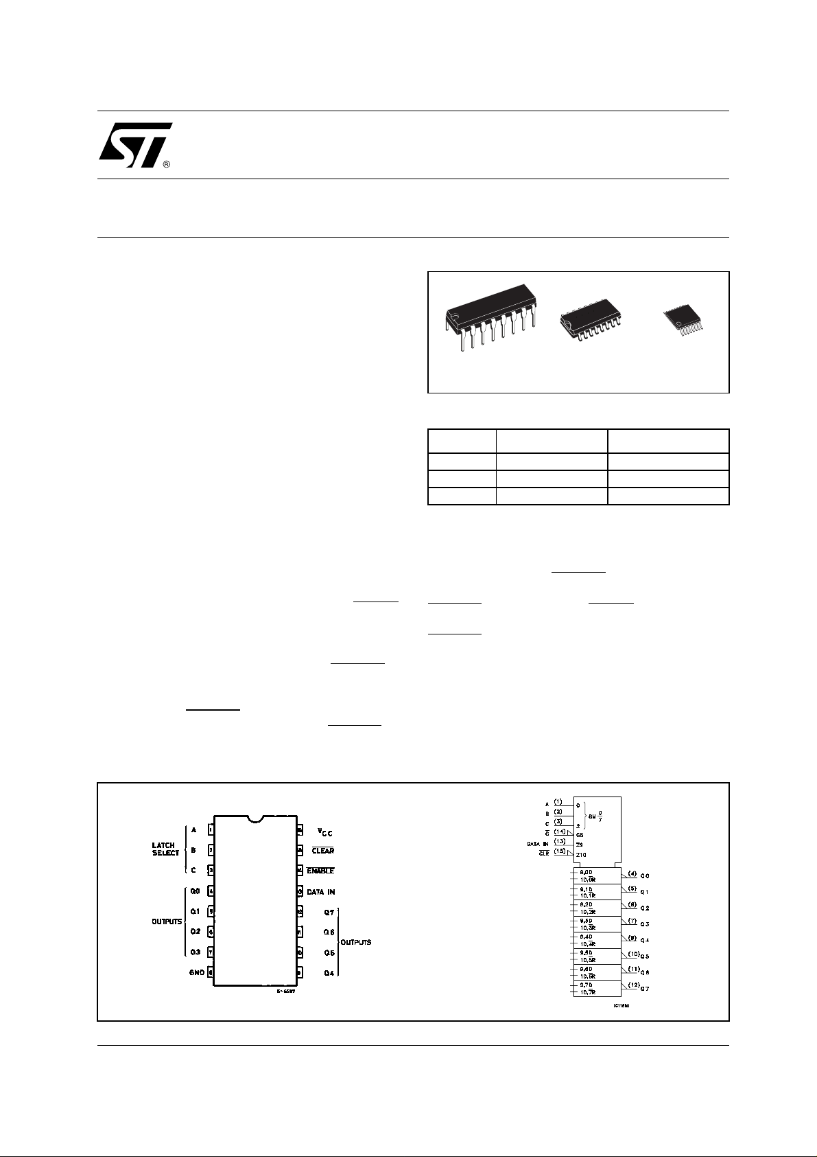
TSSOPDIP SOP
ORDER CODES
PACKAGE TUBE T & R
DIP M74HC259B1R
SOP M74HC259M1R M74HC259RM13TR
TSSOP M74HC259TTR
latches remain in their previous state, unaffect ed
by changes on the data or address inputs. To
eliminate the possibility of entering erroneous data
into the latches, th e EN A BLE
should be held high
(inactive) while the address lines are changing. If
ENABLE
is held high and CLEAR is taken l ow all
eight latches are cleared to the low state. If
ENABLE
is low all latches except the addres sed
latch will be cleared. The addressed latch will
instead follow the D input, effectively
implementing a 3-to-8 line decoder.
All inputs are equipped with protection circuits
against static discharge and transient excess
voltage.
PIN CONNECTION AND IEC LOGIC SYMBOLS
1/13July 2001
M74HC259
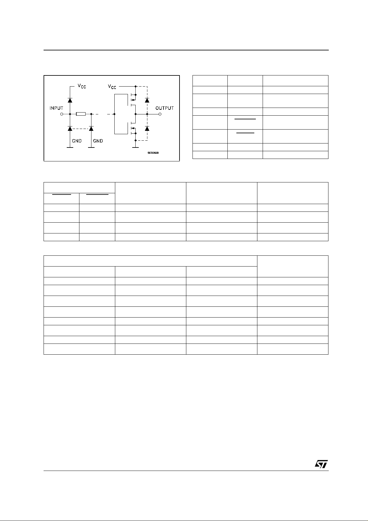
INPUT AND OUTPUT EQUIVALENT CIRCUIT PIN DESCRIPTION
PIN No SYMBOL NAME AND FUNCTION
1, 2, 3 A, B, C Address Inputs
4, 5, 6, 7, 9,
10, 11, 12
13 D Data Input
14 ENABLE
15 CLEAR
8 GND Ground (0V)
16 Vcc Positive Supply Voltage
TRUTH TABLE
Q0 to Q7 Latch Outputs
Latch Enable Input (Active
Low)
Conditional Reset Input
(Low)
INPUTS
CLEAR
H L D Qi0 ADDRESSABLE LATCH
H H Qi0 Qi0 MEMORY
L L D L 8 LINE DEMULTIPLEXER
LH L L CLEAR ALL BITS TO ’L’
D : The level at the data input
Qi0 : The level before the indicated steady state input conditions where established, (i = 0, 1, ......., 7).
ENABLE
CBA
LLLQ0
LLHQ1
LHLQ2
LHHQ3
HLLQ4
HLHQ5
HHLQ6
HHHQ7
OUTPUTS OF
ADDRESSED LATCH
SELECT INPUTS
EACH OTHER OUTPUT FUNCTION
LATCH ADDRESSED
2/13
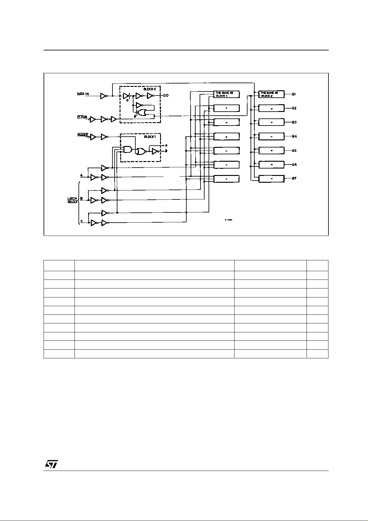
LOGIC DIAGRAM
M74HC259
This log i c diagram has not be used to est i m at e propagation delays
ABSOLUTE MAXIMUM RATINGS
Symbol Parameter Value Unit
V
V
V
I
I
OK
I
I
or I
CC
P
T
T
Absolute Maximum Ratings are those values beyond which damage to the device may occur. Functional operation under these conditions is
not implied
(*) 500mW at 65
Supply Voltage
CC
DC Input Voltage -0.5 to VCC + 0.5
I
DC Output Voltage -0.5 to VCC + 0.5
O
DC Input Diode Current
IK
DC Output Diode Current
DC Output Current
O
DC VCC or Ground Current
GND
Power Dissipation
D
Storage Temperature
stg
Lead Temperature (10 sec)
L
°C; derate to 300mW by 10mW/°C from 65°C to 85°C
-0.5 to +7 V
V
V
± 20 mA
± 20 mA
± 25 mA
± 50 mA
500(*) mW
-65 to +150 °C
300 °C
3/13
M74HC259
RECOMMENDED OPERATING CONDITIONS
Symbol Parameter Value Unit
V
V
V
T
t
r
DC SPECIFICATIONS
Symbol Parameter
V
IH
V
IL
V
OH
V
OL
I
I
I
CC
Supply Voltage
CC
Input Voltage 0 to V
I
Output Voltage 0 to V
O
Operating Temperature
op
Input Rise and Fall Time VCC = 2.0V
, t
f
V
V
CC
CC
= 4.5V
= 6.0V
Test Condition Value
= 25°C
T
A
Min. Typ. Max. Min. Max. Min. Max.
High Level Input
V
CC
(V)
2.0 1.5 1.5 1.5
Voltage
6.0 4.2 4.2 4.2
Low Level Input
2.0 0.5 0.5 0.5
Voltage
6.0 1.8 1.8 1.8
High Level Output
Voltage
Low Level Output
Voltage
Input Leakage
Current
Quiescent Supply
Current
2.0
4.5
6.0
4.5
6.0
2.0
4.5
6.0
4.5
6.0
6.0
6.0
IO=-20 µA
I
=-20 µA
O
I
=-20 µA
O
I
=-4.0 mA
O
I
=-5.2 mA
O
IO=20 µA
I
=20 µA
O
I
=20 µA
O
I
=4.0 mA
O
I
=5.2 mA
O
= VCC or GND
V
I
= VCC or GND
V
I
1.9 2.0 1.9 1.9
4.4 4.5 4.4 4.4
5.9 6.0 5.9 5.9
4.18 4.31 4.13 4.10
5.68 5.8 5.63 5.60
0.0 0.1 0.1 0.1
0.0 0.1 0.1 0.1
0.0 0.1 0.1 0.1
0.17 0.26 0.33 0.40
0.18 0.26 0.33 0.40
± 0.1 ± 1 ± 1 µA
44080µA
2 to 6 V
CC
CC
-55 to 125 °C
0 to 1000 ns
0 to 500 ns
0 to 400 ns
-40 to 85°C -55 to 125°C
V
V
Unit
V4.5 3.15 3.15 3.15
V4.5 1.35 1.35 1.35
V
V
4/13

AC ELECTRICAL CHARACTERISTICS (CL = 50 pF, Input tr = tf = 6ns)
Test Condition Value
T
Symbol Parameter
t
TLH tTHL
t
PLH tPHL
Output Transition
Time
Propagation Delay
Time
(DATA - Q)
t
PLH tPHL
Propagation Delay
Time
(A, B, C - Q)
t
PLH tPHL
t
PLH tPHL
tW(L)
t
W(L)
Propagation Delay
Time
- Q)
(G
Propagation Delay
Time
(CLEAR
Minimum Pulse
Width (ENABLE
Minimum Pulse
Width (CLEAR
Minimum Set-up
t
s
Time (DATA)
- Q)
Minimum Set-up
t
s
Time (A, B, C)
Minimum Hold
t
h
Time (DATA)
Minimum Hold
t
h
Time (A, B, C)
V
CC
(V)
2.0 30 75 95 110
6.0 7131619
2.0 56 140 175 210
6.0 15 24 30 36
2.0 76 190 240 285
6.0 20 32 41 48
2.0 57 150 190 225
6.0 16 26 32 38
2.0 45 115 145 175
6.0 13 20 25 30
2.0 28 75 90 115
)
6.0 6131620
2.0 24 75 90 115
)
6.0 5131620
2.0 12 50 60 75
6.0 3 9 11 13
2.0 25 30 40
6.0 5 5 7
2.0 5 5 5
6.0 5 5 5
2.0 0 0 0
6.0 0 0 0
= 25°C
A
Min. Typ. Max. Min. Max. Min. Max.
M74HC259
-40 to 85°C -55 to 125°C
Unit
ns4.5 8151922
ns4.5 18 28 35 42
ns4.5 24 38 48 57
ns4.5 19 30 38 45
ns4.5 15 23 29 35
ns4.5 7151923
ns4.5 6151923
ns4.5 3101215
ns4.5 5 6 8
ns4.5 5 5 5
ns4.5 0 0 0
CAPACITIVE CHARACTERISTICS
Test Condition Value
T
Symbol Parameter
V
CC
(V)
C
C
1) CPD is defined as the value of the IC’s internal equivalent capacitance which is calculated from the operating current consumption without
load. (R ef er to Test Circui t). Averag e operating current can be obtained by the following equation. I
Input Capacitance
IN
Power Dissipation
PD
Capacitance (note 1)5.0 66 pF
5.0 5101010pF
= 25°C
A
Min. Typ. Max. Min. Max. Min. Max.
-40 to 85°C -55 to 125°C
= CPD x VCC x fIN + I
CC(opr)
CC
Unit
5/13

M74HC259
TEST CIRCUIT
CL = 50pF or equivalent (includes jig and p robe capacit ance)
= Z
R
WAVEFORM 1: PROPAGATION DELAY TIME (f=1 MHz; 50% duty cycl e )
of pulse generator (typically 50Ω)
T
OUT
6/13

WAVEFORM 2 : PROPAGATION DELAY TIME (f=1MHz; 50% duty cycle)
M74HC259
WAVEFORM 3 : MINIMUM PULSE WIDTH (G
cycle)
), SETUP AND HOLD TIME (D TO G)(f=1MHz; 50% duty
7/13

M74HC259
WAVEFORM 4 : MINIMUM PULSE WIDTH (CLR) (f=1MHz; 50% duty cycle)
WAVEFORM 5 : SETUP AND HOLD TIME (f=1MHz; 50% duty cycle)
8/13

WAVEFOR M 6 : I N P U T WA VEFORMS (f=1MHz; 50% duty cycle)
M74HC259
9/13

M74HC259
Plastic DIP-16 (0.25) MECHANICAL DATA
mm. inch
DIM.
MIN. TYP MAX. MIN. TYP. MAX.
a1 0.51 0.020
B 0.77 1.65 0.030 0.065
b 0.5 0.020
b1 0.25 0.010
D 20 0.787
E 8.5 0.335
e 2.54 0.100
e3 17.78 0.700
F 7.1 0.280
I 5.1 0.201
L 3.3 0.130
Z 1.27 0.050
10/13
P001C

SO-16 MECHANICAL DATA
M74HC259
DIM.
A 1.75 0.068
a1 0.1 0.2 0.003 0.007
a2 1.65 0.064
b 0.35 0.46 0.013 0.018
b1 0.19 0.25 0.007 0.010
C 0.5 0.019
c1 45° (typ.)
D 9.8 10 0.385 0.393
E 5.8 6.2 0.228 0.244
e 1.27 0.050
e3 8.89 0.350
F 3.8 4.0 0.149 0.157
G 4.6 5.3 0.181 0.208
L 0.5 1.27 0.019 0.050
M 0.62 0.024
S8° (max.)
MIN. TYP MAX. MIN. TYP. M AX.
mm. inch
PO13H
11/13

M74HC259
TSSOP16 MECHANICAL DATA
mm. inch
DIM.
MIN. TYP MAX. MIN. TYP. M AX.
A 1.2 0.047
A1 0.05 0.15 0.002 0.004 0.006
A2 0.8 1 1.05 0.031 0.039 0.041
b 0.19 0.30 0.007 0.012
c 0.09 0.20 0.004 0.0089
D 4.9 5 5.1 0.193 0.197 0.201
E 6.2 6.4 6.6 0.244 0.252 0.260
E1 4.3 4.4 4.48 0.169 0.173 0.176
e 0.65 BSC 0.0256 BSC
K0° 8°0° 8°
L 0.45 0.60 0.75 0.018 0.024 0.030
A2
A
A1
b
e
c
K
L
E
D
E1
PIN 1 IDENTIFICATION
12/13
1
0080338D

M74HC259
Information furnished is bel ieved to be accurate and reliable. However, STMicroe lectronics assumes no responsibility for the
consequences of use of such information nor for any infringement of patents or other rights of third parties which may result from
its use. No li cense is granted by imp lication or otherwise under a ny patent or patent rig hts of STMicroelectronics. Spec ific at ions
mentioned in this publication ar e subject to change without notice. This publication supersedes and replaces all information
previously supplied. S TMicroelectronics products are not authorized for use as critica l components in life suppo rt devices or
systems without express written approval of STMicroelectronics.
Australi a - Brazil - Chi na - Finland - F rance - Germany - Hong Kon g - I ndia - Italy - Japan - Malay sia - Malta - Morocco
© The ST logo is a registered trademark of STMicroelectronics
© 2001 STM icroelectronics - Printed in Ital y - All Rights Reserved
STMicr o el ectronics GROUP OF COMPANIES
Singapo re - Spain - Sweden - Switzerland - Uni ted Kingdom
© http://www.st.com
13/13
 Loading...