

M74HC245
OCTAL BUS TRANSCEIVER
WITH 3 STATE OUTPUTS (NON INVERTED)
■ HIGH SPEED:
t
= 10ns (TYP.) at VCC = 6V
PD
■ LOW POWER DISSIPATION:
I
= 4µA(MAX.) at TA=25°C
CC
■ HIGH NOISE IMMUNITY:
V
= V
NIH
■ SYMMETRICAL OUTPUT IMPEDANCE:
|I
| = IOL = 6mA (MIN)
OH
■ BALANCED PROPAGATION DELAYS:
≅ t
t
PLH
■ WIDE OPERATING VOLTAGE RANGE:
V
(OPR) = 2V to 6V
CC
■ PIN AND FUNCTION COMPATIBLE WITH
= 28 % VCC (MIN.)
NIL
PHL
74 SERIES 245
DESCRIPTION
The M74HC245 is an advanced high-speed
CMOS OCTAL BUS TRANSCEIVER (3-STATE)
fabricated with silicon gate C
2
MOS technology.
This IC is intended for two-way asynchronous
communication between data buses, and the
direction of data transmission is determined by
DIR input. The enable input G
can be used to
TSSOPDIP SOP
ORDER CODES
PACKAGE TUBE T & R
DIP M74HC245B1R
SOP M74HC245M1R M74HC245RM13TR
TSSOP M74HC245TTR
disable the device so that the buses are effectively
isolated.
All inputs are equipped with protection circuits
against static discharge and transient excess
voltage.
All floating bus terminals during High Z State must
be held HIGH or LOW.
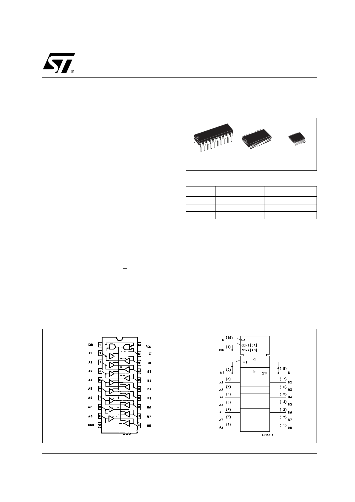
PIN CONNECTION AND IEC LOGIC SYMBOLS
1/10July 2001
M74HC245
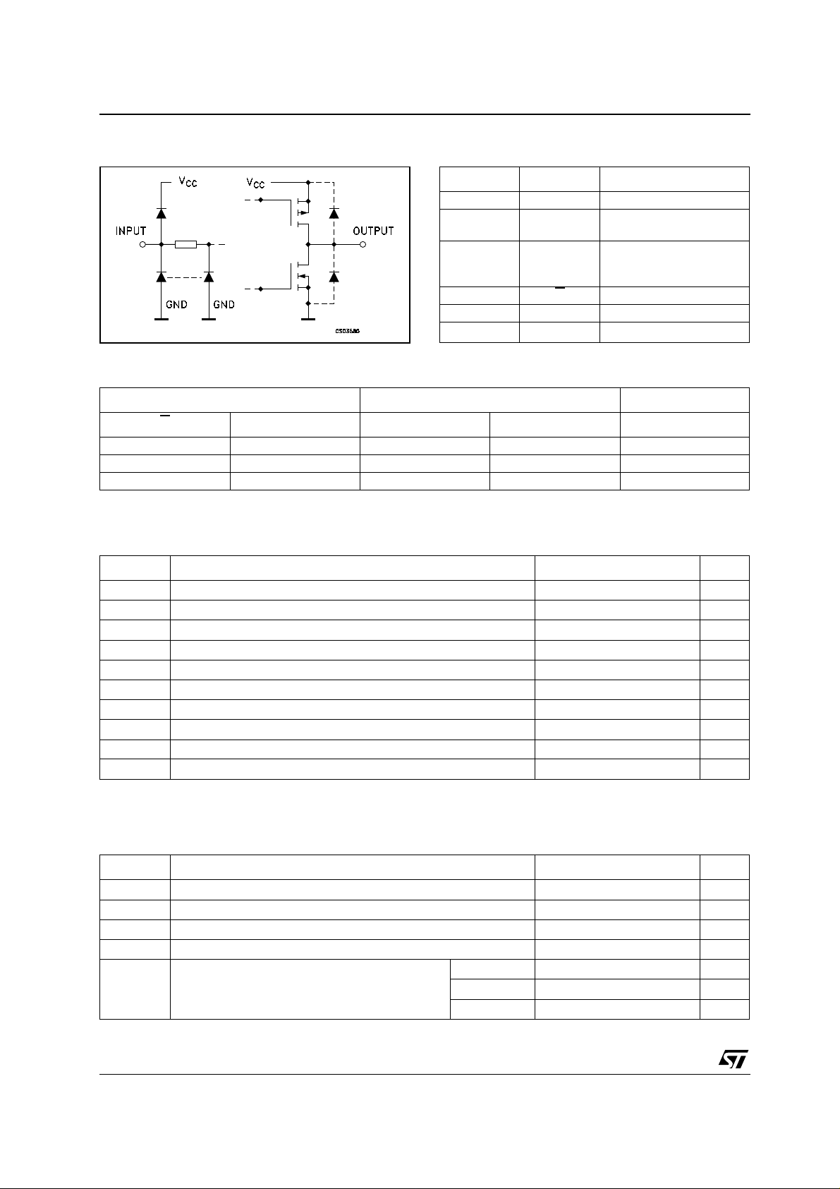
INPUT AND OUTPUT EQUIVALENT CIRCUIT PIN DESCRIPTION
PIN No SYMBOL NAME AND FUNCTION
1 DIR Directional Control
2, 3, 4, 5, 6,
7, 8, 9
18, 17, 16,
15, 14, 13,
12, 11
19 G
10 GND Ground (0V)
20 V
TRUTH TABLE
INPUTS FUNCTION OUTPUT
A1 to A8 Data Inputs/Outputs
B1 to B8 Data Inputs/Outputs
CC
Output Enable Input
Positive Supply Voltage
G
DIR A BUS B BUS Yn
L L OUTPUT INPUT A = B
L H INPUT OUTPUT B = A
HXZZZ
X : Don’t Care
Z : High Impedance
ABSOLUTE MAXIMUM RATINGS
Symbol Parameter Value Unit
V
V
V
I
I
OK
I
I
or I
CC
P
T
T
Absolute Maximum Ratings are those values beyond which damage to the device may occur. Functional operation under these conditions is
not implied
(*) 500mW at 65
Supply Voltage
CC
DC Input Voltage -0.5 to VCC + 0.5
I
DC Output Voltage -0.5 to VCC + 0.5
O
DC Input Diode Current
IK
DC Output Diode Current
DC Output Current
O
DC VCC or Ground Current
GND
Power Dissipation
D
Storage Temperature
stg
Lead Temperature (10 sec)
L
; derate to 30 0m W by 10mW/°C from 65
°C
°C to 85°C
-0.5 to +7 V
V
V
± 20 mA
± 20 mA
± 35 mA
± 70 mA
500(*) mW
-65 to +150 °C
300 °C
RECOMMENDED OPERATING CONDITIONS
Symbol Parameter Value Unit
2/10
V
V
V
T
t
r
Supply Voltage
CC
Input Voltage 0 to V
I
Output Voltage 0 to V
O
Operating Temperature
op
Input Rise and Fall Time VCC = 2.0V
, t
f
V
V
CC
CC
= 4.5V
= 6.0V
2 to 6 V
CC
CC
-55 to 125 °C
0 to 1000 ns
0 to 500 ns
0 to 400 ns
V
V
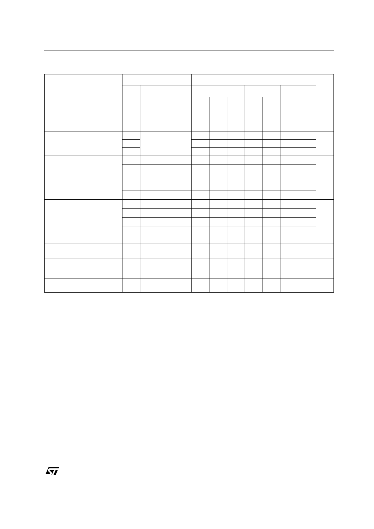
DC SPECIFICATIONS
Symbol Parameter
V
V
V
V
I
I
High Level Input
IH
Voltage
Low Level Input
IL
Voltage
High Level Output
OH
Voltage
Low Level Output
OL
Voltage
I
Input Leakage
I
Current
High Impedance
OZ
Output Leakage
Current
Quiescent Supply
CC
Current
M74HC245
Test Condition Value
T
= 25°C
V
(V)
CC
A
Min. Typ. Max. Min. Max. Min. Max.
2.0 1.5 1.5 1.5
6.0 4.2 4.2 4.2
2.0 0.5 0.5 0.5
6.0 1.8 1.8 1.8
2.0
4.5
6.0
4.5
6.0
2.0
4.5
6.0
4.5
6.0
6.0
6.0
6.0
IO=-20 µA
I
=-20 µA
O
I
=-20 µA
O
I
=-6.0 mA
O
I
=-7.8 mA
O
IO=20 µA
I
=20 µA
O
I
=20 µA
O
I
=6.0 mA
O
I
=7.8 mA
O
= VCC or GND
V
I
= VIH or V
V
I
IL
VO = VCC or GND
= VCC or GND
V
I
1.9 2.0 1.9 1.9
4.4 4.5 4.4 4.4
5.9 6.0 5.9 5.9
4.18 4.31 4.13 4.10
5.68 5.8 5.63 5.60
0.0 0.1 0.1 0.1
0.0 0.1 0.1 0.1
0.0 0.1 0.1 0.1
0.17 0.26 0.33 0.40
0.18 0.26 0.33 0.40
-40 to 85°C -55 to 125°C
± 0.1 ± 1 ± 1 µA
± 0.5 ± 5 ± 10 µA
44080µA
Unit
V4.5 3.15 3.15 3.15
V4.5 1.35 1.35 1.35
V
V
3/10
 Loading...