

M74HC174
HEX D-TYPE FLIP FLOP WITH CLEAR
■ HIGH SPEED :
f
= 66MHz (TYP.) at VCC = 6V
MAX
■ LOW POWER DISSIPATION:
I
=4µA(MAX.) at TA=25°C
CC
■ HIGH NOISE IMMUNITY:
V
= V
NIH
■ SYMMETRICAL OUTPUT IMPEDANCE:
|I
| = IOL = 4mA (MIN)
OH
■ BALANCED PROPAGATION DELAYS:
t
≅ t
PLH
■ WIDE OPERATING VOLTAGE RANGE:
V
(OPR) = 2V to 6V
CC
■ PIN AND FUNCTION COMPATIBLE WITH
= 28 % VCC (MIN.)
NIL
PHL
74 SERIES 174
DESCRIPTION
The M74HC174 is an high speed CMOS HEX
D-TYPE FLIP FLOP WITH CLEAR fabricated with
silicon gate C
2
MOS technology.
Information signals applied to D inputs are
transferred to the Q output on the positive going
edge of the clock pulse. When the CLEAR
input is
TSSOPDIP SOP
ORDER CODES
PACKAGE TUBE T & R
DIP M74HC174B1R
SOP M74HC174M1R M74HC174RM13TR
TSSOP M74HC174TTR
held low, the Q outputs are held low independently
of the other inputs.
All inputs are equipped with protection circuits
against static discharge and transient excess
voltage.
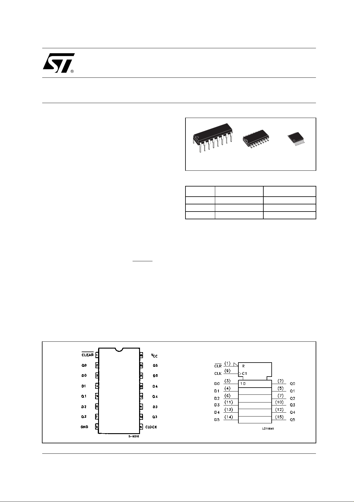
PIN CONNECTION AND IEC LOGIC SYMBOLS
1/11July 2001
M74HC174
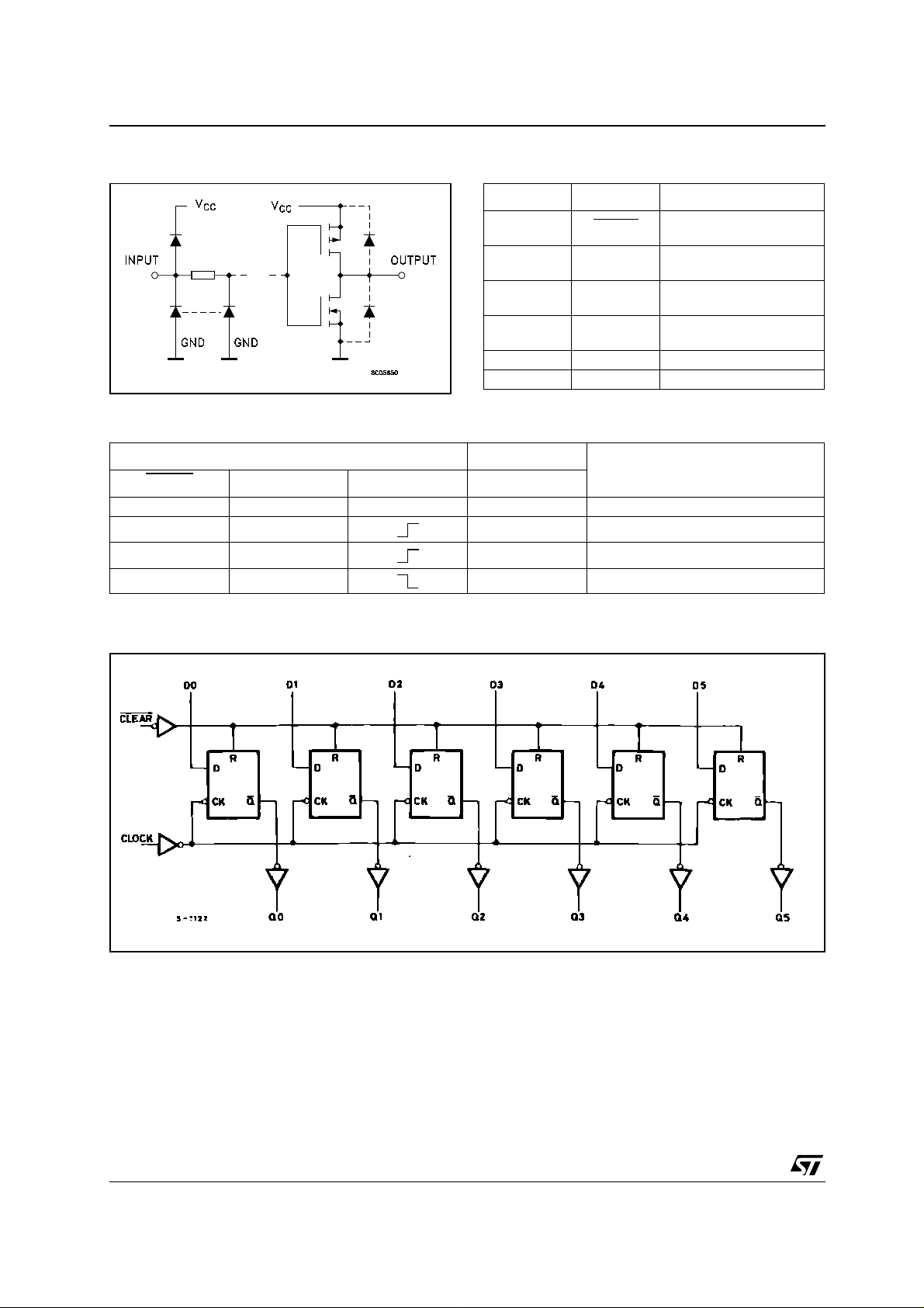
INPUT AND OUTPUT EQUIVALENT CIRCUIT PIN DESCRIPTION
PIN No SYMBOL NAME AND FUNCTION
1 CLEAR
2, 5, 7, 10,
12, 15
3, 4, 6, 11,
13, 14
9 CLOCK
8 GND Ground (0V)
16 Vcc Positive Supply Voltage
TRUTH TABLE
Q0 to Q5 Flip-Flop Outputs
D0 to D5 Data Inputs
Asynchronous Master
Reset (Active Low)
Clock Input (LOW to
HIGH, edge triggered)
CLEAR
L X X L CLEAR
HL L
HH H
H X Qn NO CHANGE
X : Don’t Care
LOGIC DIAGRAM
INPUTS OUTPUTS
FUNCTION
DCKQ
This log i c diagram has not to be used to es t i m ate propagati on delays
2/11
M74HC174
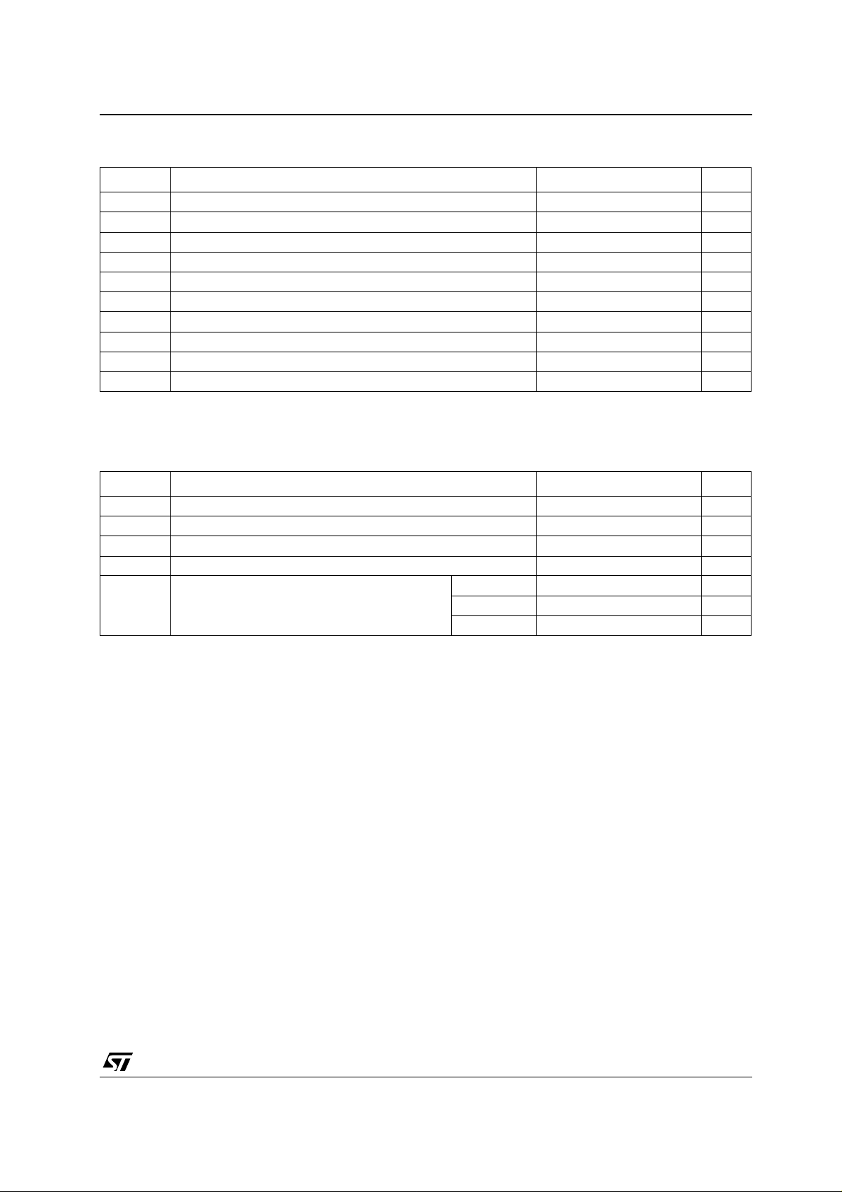
ABSOLUTE MAXIMUM RATINGS
Symbol Parame ter Value Unit
V
V
V
I
I
OK
I
I
or I
CC
P
T
T
Absolute Maximum Ratings are those values beyond which damage to the device may occur. Functional operation under these conditions is
not implied
(*) 500mW at 65
RECOMMENDED OPERATING CONDITIONS
Symbol Parameter Value Unit
V
V
V
T
t
r
Supply Voltage
CC
DC Input Voltage -0.5 to VCC + 0.5
I
DC Output Voltage -0.5 to VCC + 0.5
O
DC Input Diode Current
IK
DC Output Diode Current
DC Output Current
O
DC VCC or Ground Current
GND
Power Dissipation
D
Storage Temperature
stg
Lead Temperature (10 sec)
L
°C; derate to 300mW by 10mW/°C from 65°C to 85°C
Supply Voltage
CC
Input Voltage 0 to V
I
Output Voltage 0 to V
O
Operating Temperature
op
Input Rise and Fall Time VCC = 2.0V
, t
f
V
V
CC
CC
= 4.5V
= 6.0V
-0.5 to +7 V
± 20 mA
± 20 mA
± 25 mA
± 50 mA
500(*) mW
-65 to +150 °C
300 °C
2 to 6 V
CC
CC
-55 to 125 °C
0 to 1000 ns
0 to 500 ns
0 to 400 ns
V
V
V
V
3/11
M74HC174
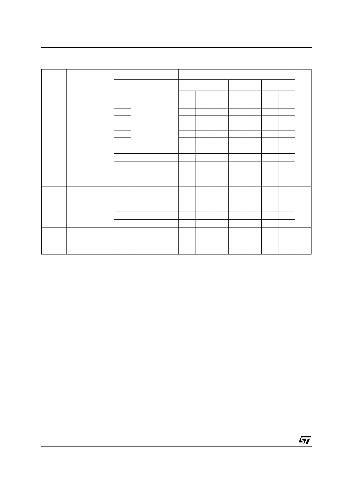
DC SPECIFICATIONS
Symbol Parameter
V
V
V
V
I
High Level Input
IH
Voltage
Low Level Input
IL
Voltage
High Level Output
OH
Voltage
Low Level Output
OL
Voltage
I
Input Leakage
I
Current
Quiescent Supply
CC
Current
Test Condition Value
V
(V)
CC
= 25°C
A
Min. Typ. Max. Min. Max. Min. Max.
-40 to 85°C -55 to 125°C
T
2.0 1.5 1.5 1.5
6.0 4.2 4.2 4.2
2.0 0.5 0.5 0.5
6.0 1.8 1.8 1.8
2.0
4.5
6.0
4.5
6.0
2.0
4.5
6.0
4.5
6.0
6.0
6.0
IO=-20 µA
I
=-20 µA
O
I
=-20 µA
O
I
=-4.0 mA
O
I
=-5.2 mA
O
IO=20 µA
I
=20 µA
O
I
=20 µA
O
I
=4.0 mA
O
I
=5.2 mA
O
= VCC or GND
V
I
= VCC or GND
V
I
1.9 2.0 1.9 1.9
4.4 4.5 4.4 4.4
5.9 6.0 5.9 5.9
4.18 4.31 4.13 4.10
5.68 5.8 5.63 5.60
0.0 0.1 0.1 0.1
0.0 0.1 0.1 0.1
0.0 0.1 0.1 0.1
0.17 0.26 0.33 0.40
0.18 0.26 0.33 0.40
± 0.1 ± 1 ± 1 µA
44080µA
Unit
V4.5 3.15 3.15 3.15
V4.5 1.35 1.35 1.35
V
V
4/11
 Loading...