

■ HIGH SPEED :
f
= 62MHz (TYP.) at VCC=6V
MAX
■ LOW POWER DISSIPATION:
I
=4µA(MAX.) at TA=25°C
CC
■ HIGH NOISE IMMUNITY:
V
NIH=VNIL
■ SYMMETRICAL OUT PUT IMPEDANCE:
|I
|=IOL=4mA(MIN)
OH
■ BALANCED PROPAGATION DELAYS:
t
≅ t
PLH
■ WIDE OPERATING VOLTAGE RANGE:
V
(OPR) = 2V to 6V
CC
■ PIN AND FUNCTION COMPATIBLE WITH
=28%VCC(MIN.)
PHL
74 SERIES 164
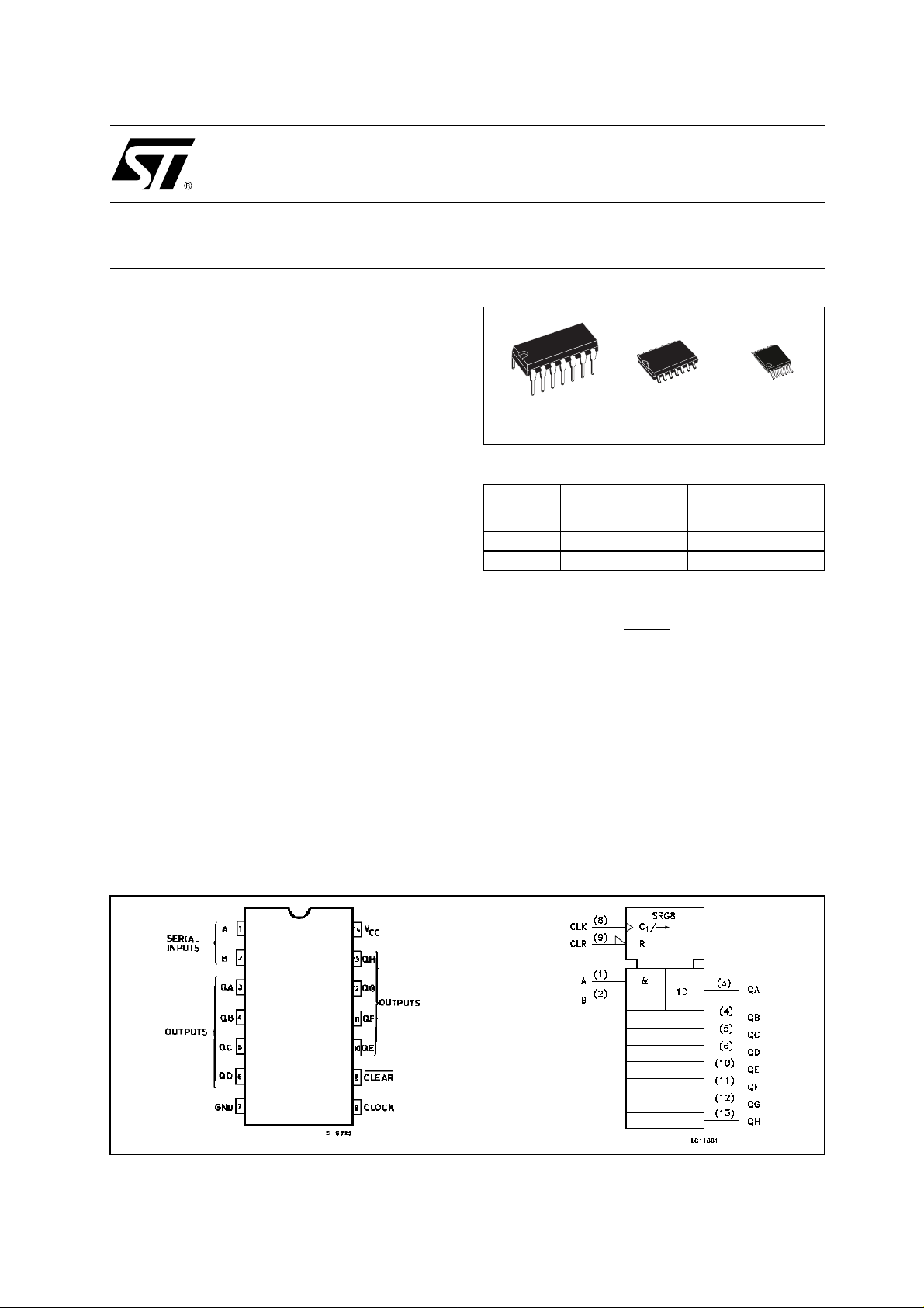
DESCRIPTION
The M74HC164 is an high speed CMOS 8 BIT
SIPO SHIFT REG ISTER fabricated with silicon
gate C
2
MOS technology.
The M74HC164 is an 8 bi t shi ft register with seria l
data entry and an output from eac h of the eight
stages. Data is entered serially through oneoftwo
inputs (A or B), either of these inputs can be used
as an active high enable for data entry through t he
other input. An unused input must be high, or both
inputs connected together. Each low-to-high
M74HC164
8 BIT SIPO SHIFT REGISTER
TSSOPDIP SOP
ORDER CODES
PACKAGE TUBE T & R
DIP M74HC164B1R
SOP M74HC164M1R M74HC164RM13TR
TSSOP M74HC164TTR
transition on the clock inputs shifts data one place
to t he right and enters into QA the logic NAND of
the two data inputs (A
before the rising clock edge. A low level on the
clear i nput overrides all other inputs and clears the
register asynchronously, forcing all Q outputs low.
All inputs are equi pped with protection circuits
against static discharge and transient excess
voltage.
x B), the data that existed
PIN CONNECTION AND IEC LOGIC SYMBOLS
1/13June 2003
M74HC164
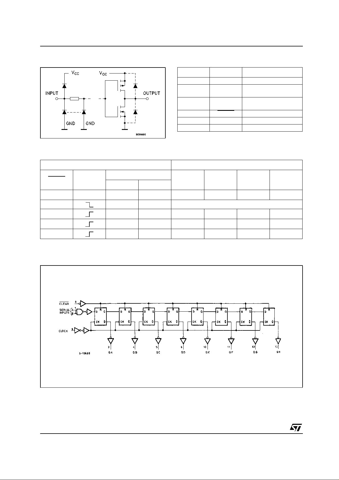
INPUT AND OUTPUT EQUIVALENT CIRCUIT PIN DESCRIPTION
PIN No SYMBOL NAME AND FUNCTION
1,2 A, B Data Inputs
3, 4, 5, 6, 10,
11, 12, 13
8 CLOCK
9 CLEAR
7 GND Ground (0V)
14 Vcc Positive Supply Voltage
TRUTH TABLE
INPUTS OUTPUTS
QA to QH Outputs
Clock Input (LOW to
HIGH, Edge Triggered
Master Reset Input
CLEAR
L X X X L L ........... L
H X X NO CHANGE
H L X L QAn ........... QGn
H X L L QAn ........... QGn
H H H H QAn ........... QGn
X : Don’tCare
QAn - QGn : The level of QA - QG, respectively. before the most-recent transition of the clock
CLOCK
SERIAL IN
QA QB ........... QH
AB
LOGIC DIAGRAM
This logic diagram has not be used to estimate propagation delays
2/13

TIMING CHART
M74HC164
ABSOLUTE MAXIMUM RATINGS
Symbol Parameter Value Unit
V
V
V
I
I
OK
I
or I
I
CC
P
T
T
Absolute Maximum Ratings are those values beyond which damage to the device may occur. Functional operation under these conditions is
not implied
(*) 500mW at 65
Supply Voltage
CC
DC Input Voltage -0.5 to VCC+ 0.5
I
DC Output Voltage -0.5 to VCC+ 0.5
O
DC Input Diode Current
IK
DC Output Diode Current
DC Output Current
O
DC VCCor Ground Current
GND
Power Dissipation
D
Storage Temperature
stg
Lead Temperature (10 sec)
L
°C; derate to 300mW by 10mW/°Cfrom65°Cto85°C
-0.5 to +7 V
V
V
± 20 mA
± 20 mA
± 25 mA
± 50 mA
500(*) mW
-65 to +150 °C
300 °C
3/13
M74HC164
RECOMMENDED OPERATING CONDITIONS
Symbol Parameter Value Unit
V
V
V
T
t
r,tf
DC SPECIFICATIONS
Symbol Parameter
V
IH
V
IL
V
OH
V
OL
I
I
I
CC
Supply Voltage
CC
Input Voltage 0 to V
I
Output Voltage 0 to V
O
Operating Temperature
op
Input Rise and Fall Time VCC= 2.0V
= 4.5V
V
CC
= 6.0V
V
CC
Test Condition Value
= 25°C
T
A
Min. Typ. Max. Min. Max. Min. Max.
High Level Input
V
CC
(V)
2.0 1.5 1.5 1.5
Voltage
6.0 4.2 4.2 4.2
Low Level Input
2.0 0.5 0.5 0.5
Voltage
6.0 1.8 1.8 1.8
High Level Output
Voltage
Low Level Output
Voltage
Input Leakage
Current
Quiescent Supply
Current
2.0
4.5
6.0
4.5
6.0
2.0
4.5
6.0
4.5
6.0
6.0
6.0
I
I
I
I
O
I
O
I
I
V
I=VCC
V
I=VCC
=-20 µA
O
=-20 µA
O
=-20 µA
O
=-4.0 mA
=-5.2 mA
=20 µA
I
O
=20 µA
I
O
I
=20 µA
O
=4.0 mA
O
=5.2 mA
O
or GND
or GND
1.9 2.0 1.9 1.9
4.4 4.5 4.4 4.4
5.9 6.0 5.9 5.9
4.18 4.31 4.13 4.10
5.68 5.8 5.63 5.60
0.0 0.1 0.1 0.1
0.0 0.1 0.1 0.1
0.0 0.1 0.1 0.1
0.17 0.26 0.33 0.40
0.18 0.26 0.33 0.40
± 0.1 ± 1 ± 1 µA
44080µA
2to6 V
CC
CC
-55 to 125 °C
0 to 1000 ns
0 to 500 ns
0 to 400 ns
-40 to 85°C -55 to 125°C
V
V
Unit
V4.5 3.15 3.15 3.15
V4.5 1.35 1.35 1.35
V
V
4/13

AC ELECTRICAL CHARACTERISTICS (CL= 50 pF, Input tr=tf=6ns)
Test Condition Value
= 25°C
Symbol Parameter
t
TLHtTHL
t
PLHtPHL
t
PLHtPHL
f
t
W(H)
t
t
t
REM
Output Transition
Time
Propagation Delay
Time (CLOCK - Q)
Propagation Delay
Time (CLEAR
Maximum Clock
MAX
Frequency
Minimum Pulse
Width (CLOCK)
W(L)
Minimum Pulse
W(L)
Width (CLEAR
t
Set-up Time (A, B -
s
CK)
t
Hold Time (A, B -
h
CK)
Minimum Removal
Time
-Q)
)
V
CC
(V)
2.0 30 75 95 110
6.0 7 13 16 19
2.0 57 160 200 240
6.0 16 27 34 41
2.0 60 175 220 265
6.0 17 30 37 45
2.0 6.2 18 5.0 4.2
6.0 37 62 30 25
2.0 24 75 95 110
6.0 5 13 16 19
2.0 40 75 95 110
6.0 9 13 16 19
2.0 50 65 75
6.0 9 11 13
2.0 5 5 5
6.0 5 5 5
2.0 5 5 5
6.0 5 5 5
T
A
Min. Typ. Max. Min. Max. Min. Max.
M74HC164
-40 to 85°C -55 to 125°C
Unit
ns4.5 8 15 19 22
ns4.5 19 32 40 48
ns4.5 20 35 44 53
MHz4.5 31 53 25 21
ns4.5 6 15 19 22
ns4.5 10 15 19 22
ns4.5 10 13 15
ns4.5 5 5 5
ns4.5 5 5 5
CAPACITIVE CHARACTERISTICS
Test Condition Value
= 25°C
Symbol Parameter
V
CC
(V)
C
C
1) CPDis defined as the value of the IC’s internal equivalent capacitance which is calculated from the operating current consumption without
load. (Refer to Test Circuit). Average operating current can be obtained by the following equation. I
Input Capacitance
IN
Power Dissipation
PD
Capacitance (note1)5.0 99 pF
5.0 5 10 10 10 pF
T
A
-40 to 85°C -55 to 125°C
Min. Typ. Max. Min. Max. Min. Max.
CC(opr)=CPDxVCCxfIN+ICC
Unit
5/13

M74HC164
TEST CIRCUIT
CL= 50pF or equivalent (includes jig and probe capacitance)
R
T=ZOUT
WAVEFORM 1: MINIMUMPULSEWIDTH(CLEAR),MINIMUM REMOVAL TIME (CLEAR TO CLOC K)
(f=1MHz; 50% duty cycle)
of pulse generator (typically 50Ω)
6/13

M74HC164
WAVEFORM 2 : PROPAGATION DEL AY TIMES, M I NIMUM P UL S E WIDTH (CLOCK), S ETUP AND
HOLD TIME (A,B TO CLOCK) (f=1MHz ; 50% duty cycle)
7/13

M74HC164
Plastic DIP-14 MECHANICAL DATA
mm. inch
DIM.
MIN. TYP MAX. MIN. TYP. MAX.
a1 0.51 0.020
B 1.39 1.65 0.055 0.065
b 0.5 0.020
b1 0.25 0.010
D 20 0.787
E 8.5 0.335
e 2.54 0.100
e3 15.24 0.600
F 7.1 0.280
I 5.1 0.201
L 3.3 0.130
Z 1.27 2.54 0.050 0.100
8/13
P001A

SO-14 MECHANICAL DATA
M74HC164
DIM.
A 1.75 0.068
a1 0.1 0.2 0.003 0.007
a2 1.65 0.064
b 0.35 0.46 0.013 0.018
b1 0.19 0.25 0.007 0.010
C 0.5 0.019
c1 45˚ (typ.)
D 8.55 8.75 0. 336 0.344
E 5.8 6.2 0.228 0.244
e 1.27 0.050
e3 7.62 0.300
F 3.8 4.0 0.149 0.157
G 4.6 5.3 0.181 0.208
L 0.5 1.27 0.019 0. 050
M 0.68 0.026
S ˚ (max.)
MIN. TYP MAX. MIN. TYP. MAX.
mm. inch
8
PO13G
9/13

M74HC164
TSSOP14 MECHANICAL DATA
mm. inch
DIM.
MIN. TYP MAX. MIN. TYP. MAX.
A 1.2 0.047
A1 0.05 0.15 0.002 0.004 0.006
A2 0.8 1 1.05 0.031 0.039 0.041
b 0.19 0.30 0.007 0.012
c 0.09 0.20 0.004 0.0089
D 4.9 5 5.1 0.193 0.197 0.201
E 6.2 6.4 6.6 0.244 0.252 0.260
E1 4.3 4.4 4.48 0.169 0.173 0.176
e 0.65 BSC 0.0256 BSC
K0˚ 8˚0˚ 8˚
L 0.45 0.60 0.75 0.018 0.024 0.030
A2
A
A1
b
e
c
K
L
E
D
E1
PIN 1 IDENTIFICATION
10/13
1
0080337D

M74HC164
Tape & Reel SO-14 MECHANICAL DATA
mm. inch
DIM.
MIN. TYP MAX. MIN. TYP. MAX.
A 330 12.992
C 12.8 13.2 0.504 0.519
D 20.2 0.795
N 60 2.362
T 22.4 0.882
Ao 6.4 6.6 0.252 0.260
Bo 9 9.2 0.354 0.362
Ko 2.1 2.3 0.082 0.090
Po 3.9 4.1 0.153 0.161
P 7.9 8.1 0.311 0.319
11/13

M74HC164
Tape & Reel TSSOP14 MECHANICAL DATA
mm. inch
DIM.
MIN. TYP MAX. MIN. TYP. MAX.
A 330 12.992
C 12.8 13.2 0.504 0.519
D 20.2 0.795
N 60 2.362
T 22.4 0.882
Ao 6.7 6.9 0.264 0.272
Bo 5.3 5.5 0.209 0.217
Ko 1.6 1.8 0.063 0.071
Po 3.9 4.1 0.153 0.161
P 7.9 8.1 0.311 0.319
12/13

M74HC164
Information furnished is believed to be accurate and reliable . However, STMicroelectronics assumes no responsibility for the
consequences of use o f suc h inf ormat ion n or f or an y infr ingeme nt of paten ts or oth er ri gh ts of third part ies whic h may resul t f rom
its use. No license is granted by implication or otherwise under any patent or patent rights of STMicroelectronics. Specifications
mentioned in this publication are subject to change without notice. This publication supersedes and replaces all information
previously supplied. STMicroelectronics products are not authorized for use as critical components in life support devices or
systems without express written approval of STMicroelectronics.
Australia - Brazil - Canada - China - Finland - France - Germany - Hong Kong - India - Israel - Italy - Japan - Malaysia - Malta - Morocco
© The ST logo is a registered trademark of STMicroelectronics
© 2003 STMicroelectronics - Printed in Italy - All Rights Reserved
STMicroelectronics GROUP OF COMPANIES
Singapore - Spain - Sweden - Switzerland - United Kingdom - United States.
© http://www.st.com
13/13
 Loading...