


M74HC132
QUAD 2-INPUT SCHMITT NAND GATE
■ HIGH SPEED:
t
= 11ns (TYP.) at VCC = 6V
PD
■ LOW POWER DISSIPATION:
I
= 1µA(MAX.) at TA=25°C
CC
■ HIGH NOISE IMMUNITY:
V
(TYP.) = 0.9 V AT VCC = 5 V
H
■ SYMMETRICAL OUTPUT IMPEDANCE:
|I
| = IOL = 4mA (MIN)
OH
■ BALANCED PROPAGATION DELAYS:
t
≅ t
PLH
■ WIDE OPERATING VOLTAGE RANGE:
V
CC
■ PIN AND FUNCTION COMPATIBLE WITH
PHL
(OPR) = 2V to 6V
74 SERIES 132
DESCRIPTION
The M74HC132 is an high speed CMOS QUAD
2-INPUT SCHMITT NAND GATE fabricated with
silicon gate C
2
MOS technology.
Pin configuration and function are identical to
those of the M74HC00.
The hysteresis characteristics (around 20% V
cc
of all inputs allow slowly changing input signals t o
TSSOPDIP SOP
ORDER CODES
PACKAGE TUBE T & R
DIP M74HC132B1R
SOP M74HC132M1R M74HC132RM13TR
TSSOP M74HC132TTR
be transformed into sharply defined jitter-free
output signals.
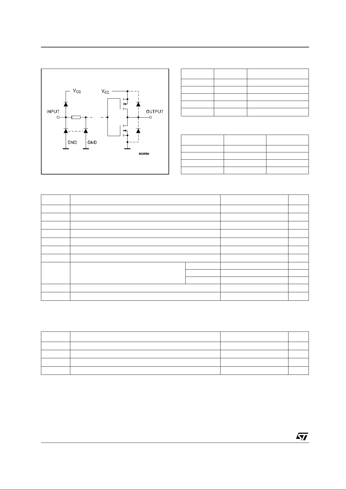
All inputs are equipped with protection circuits
against static discharge and transient excess
voltage.
)
PIN CONNECTION AND IEC LOGIC SYMBOLS
1/9March 2002
M74HC132
INPUT AND OUTPUT EQUIVALENT CIRCUIT PIN DESCRIPTION
PIN No SYMBOL NAME AND FUNCTION
1, 4, 9, 12 1A to 4A Data Inputs
2, 5, 10, 13 1B to 4B Data Inputs
3, 6, 8, 11 1Y to 4Y Data Outputs
7 GND Ground (0V)
14
V
CC
TRUTH TABLE
ABY
LLH
LHH
HLH
HHL
ABSOLUTE MAXIMUM RATINGS
Symbol Parameter Value Unit
V
V
V
I
I
OK
I
or I
I
CC
P
T
T
Absolute Maximum Ratings are those values beyond which damage to the device may occur. Functional operation under these conditions is
not implied
(*) Power difssipation at 65
Supply Voltage
CC
DC Input Voltage -0.5 to VCC + 0.5
I
DC Output Voltage -0.5 to VCC + 0.5
O
DC Input Diode Current
IK
DC Output Diode Current
DC Output Current
O
DC VCC or Ground Current
GND
Power Dissipation DIP 750(*) mW
D
SOP 500(*) mW
TSSOP 450(*) mW
Storage Temperature
stg
Lead Temperature (10 sec)
L
°C. Derating from 65°C to 125°C: DIP Package -10mW/° C; SO Pa ck age - 7mW/° C; TSSOP Pac kage -6 .1mW/°C
Positive Supply Voltage
-0.5 to +7 V
20 mA
±
20 mA
±
25 mA
±
50 mA
±
-65 to +150 °C
300 °C
V
V
RECOMMENDED OPERATING CONDITIONS
Symbol Parameter Value Unit
V
V
V
T
2/9
Supply Voltage
CC
Input Voltage 0 to V
I
Output Voltage 0 to V
O
Operating Temperature
op
2 to 6 V
CC
CC
-55 to 125 °C
V
V
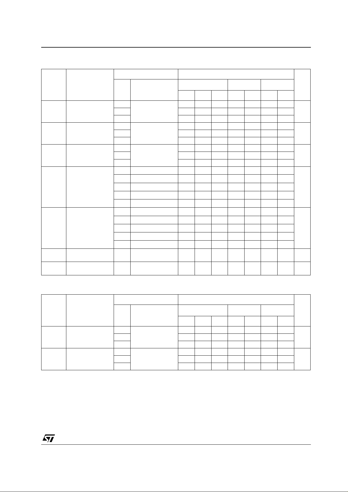
DC SPECIFICATIONS
Symbol Parameter
V
High Level
P
Threshold Voltage
Low Level
V
N
Threshold Voltage
Hysteresis Voltage 2.0 0.3 0.6 1.0 0.3 1.0 0.3 1.0
V
H
V
V
I
High Level Output
OH
Voltage
Low Level Output
OL
Voltage
I
Input Leakage
I
Current
Quiescent Supply
CC
Current
M74HC132
Test Condition Value
T
= 25°C
V
CC
(V)
A
Min. Typ. Max. Min. Max. Min. Max.
2.0 1.0 1.25 1.5 1.0 1.5 1.0 1.5
6.0 3.0 3.5 4.2 3.0 4.2 3.0 4.2
2.0 0.3 0.65 0.9 0.3 0.9 0.3 0.9
6.0 1.5 2.3 2.6 1.5 2.6 1.5 2.6
6.0 0.8 1.2 1.4 0.8 1.7 0.8 1.7
=-20 µA
2.0
4.5
6.0
4.5
6.0
2.0
4.5
6.0
4.5
6.0
6.0
6.0
I
O
I
=-20 µA
O
I
=-20 µA
O
I
=-4.0 mA
O
I
=-5.2 mA
O
IO=-20 µA
I
=-20 µA
O
I
=-20 µA
O
I
=-4.0 mA
O
I
=-5.2 mA
O
= VCC or GND
V
I
= VCC or GND
V
I
1.9 2.0 1.9 1.9
4.4 4.5 4.4 4.4
5.9 6.0 5.9 5.9
4.18 4.31 4.13 4.10
5.68 5.8 5.63 5.60
0.0 0.1 0.1 0.1
0.0 0.1 0.1 0.1
0.0 0.1 0.1 0.1
0.17 0.26 0.33 0.40
0.18 0.26 0.33 0.40
-40 to 85°C -55 to 125°C
±
0.1
1
±
±
11020
Unit
1
V4.5 2.3 2.7 3.15 2.3 3.15 2.3 3.15
V4.5 1.13 1.6 2.0 1.13 2.0 1.13 2.0
V4.5 0.6 1.1 1.4 0.6 1.4 0.6 1.4
V
V
A
µ
A
µ
AC ELECTRICAL CHARACTERISTICS (C
Test Condition Value
Symbol Parameter
t
TLH tTHL
t
PLH tPHL
Output Transition
Time
Propagation Delay
Time
V
CC
(V)
2.0 30 75 95 110
6.0 7131619
2.0 52 105 130 160
6.0 11 18 22 27
= 50 pF, Input tr = tf = 6ns)
L
T
= 25°C
A
Min. Typ. Max. Min. Max. Min. Max.
-40 to 85°C -55 to 125°C
Unit
ns4.5 8151922
ns4.5 13 21 26 32
3/9
 Loading...