

M74HC123
DUAL RETRIGGERABLE MONOSTABLE MULTIVIBRATOR
■ HIGH SPEED :
t
= 23 ns (TYP.) at VCC = 6V
PD
■ LOW POWER DISSIPATION:
STAND BY STATE :
I
=4µA (MAX.) at TA=25°C
CC
ACTIVE STATE :
I
=200µA (MAX.) at V
CC
■ HIGH NOISE IMMUNITY:
V
= V
NIH
■ SYMMETRICAL OUTPUT IMPEDANCE:
|I
| = IOL = 4mA (MIN)
OH
■ BALANCED PROPAGATION DELAYS:
t
≅ t
PLH
■ WIDE OPERATING VOLTAGE RANGE:
V
(OPR) = 2V to 6V
CC
■ WIDE OUTPUT PULSE WIDTH RANGE :
t
WOUT
■ PIN AND FUNCTION COMPATIBLE WITH
= 28 % VCC (MIN.)
NIL
PHL
= 120 ns ~ 60 s OVER AT V
CC
= 5V
CC
= 4.5 V
74 SERIES 123
DESCRIPTION
The M74HC123 is an high speed CMOS
MONOSTABLE MULTIVIBRATOR fabricated with
silicon gate C
There are two trigger inputs, A
2
MOS technology.
INPUT (negative
edge) and B I NP UT (pos itive edg e). These inputs
are valid for slow rising/falling signals, (tr=tf=l sec).
The device may also be triggered by using the
CLR
input (positive-edge) because of the
Schmitt-trigger input; after triggering the output
maintains the MONOSTABLE state for the time
TSSOPDIP SOP
ORDER CODES
PACKAGE TUBE T & R
DIP M74HC123B1R
SOP M74HC123M1R M74HC123RM13TR
TSSOP M74HC123TTR
period determined by the ex ternal resistor Rx a nd
capacitor Cx. When Cx >
10nF and Rx > 10KΩ,
the output pulse width value is approsimatively
given by the formula : tW(OUT) = K · Cx · Rx.
(K
≅ 0.45).
Taking CLR
low breaks this MONOSTABLE
STATE. If the next trigger pul se oc curs du ring the
MONOSTABLE period it makes the
MONOSTABLE period longer. Limit for values of
Cx and Rx : Cx : NO LIMIT
Rx : V
V
< 3.0V 5KΩ to 1MΩ
cc
> 3.0V 1KΩ to 1MΩ
cc
All inputs are equipped with protection circuits
against static discharge and transient excess
voltage.
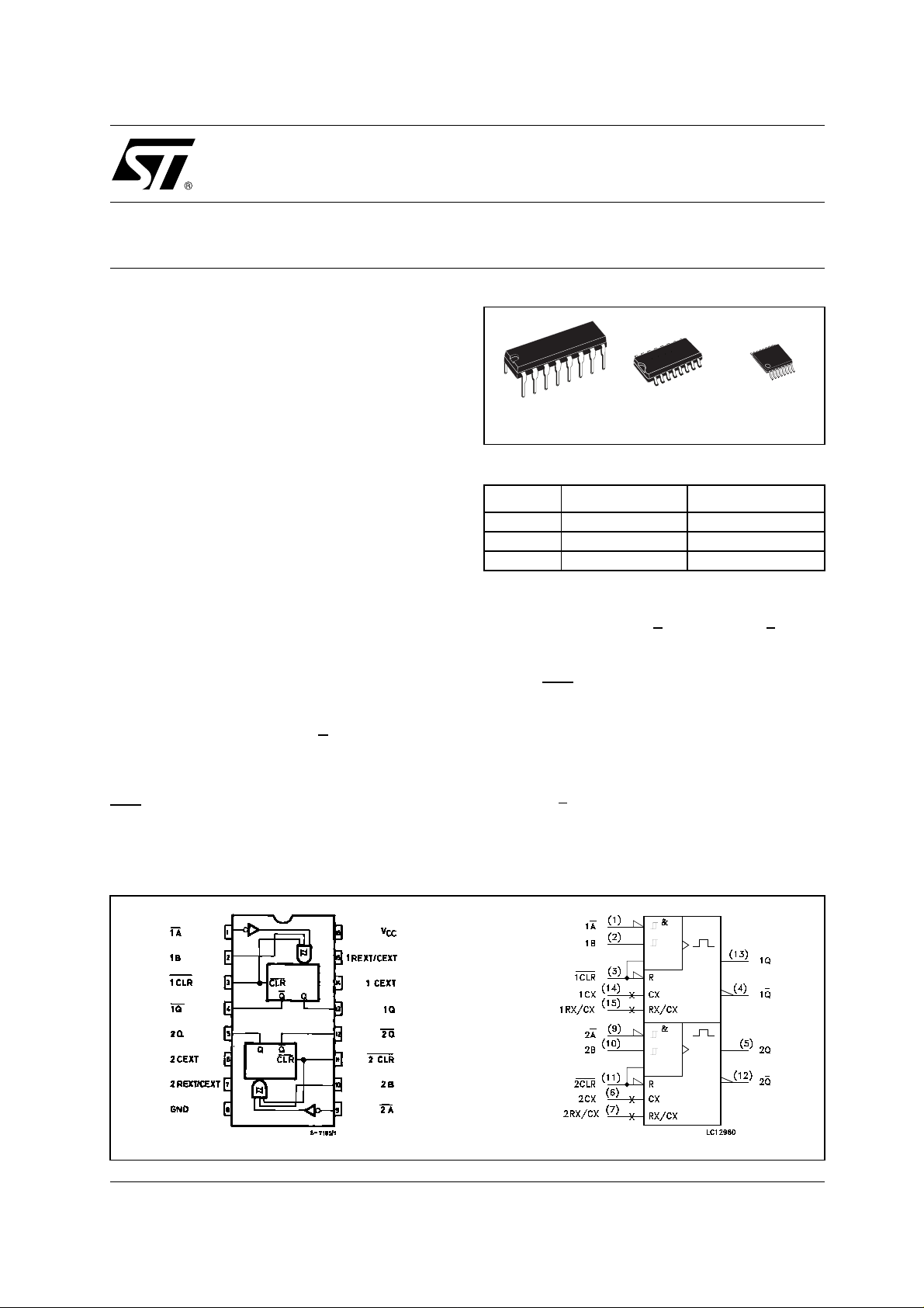
PIN CONNECTION AND IEC LOGIC SYMBOLS
1/12July 2001

M74HC123
INPUT AND OUTPUT EQUIVALENT CIRCUIT PIN DESCRIPTION
PIN No SYMBOL NAME AND FUNCTION
1,9 1A
2, 10 1B, 2B
3, 11
4, 12 1Q
7
13, 5 1Q, 2Q Outputs (Active High)
14, 6
15
8 GND Ground (0V)
16 Vcc Positive Supply Voltage
TRUTH TABLE
, 2A
1 CLR
2 CLR
, 2Q Outputs (Active Low)
2R
X/CX
1C
X
2C
X
1R
X/CX
Trigger Inputs (Negative
Edge Triggered)
Trigger Inputs (Positive
Edge Triggered)
Direct Reset LOW and
trigger Action at Positive
Edge
External Resistor
Capacitor Connection
External Capacitor
Connection
External Resistor
Capacitor Connection
INPUTS OUTPUTS
A
BCLRQQ
H H OUTPUT ENABLE
X L H L H INHIBIT
H X H L H INHIBIT
L H OUTPUT ENABLE
L H OUTPUT ENABLE
X X L L H INHIBIT
X : Don’t Care
NOTE
2/12
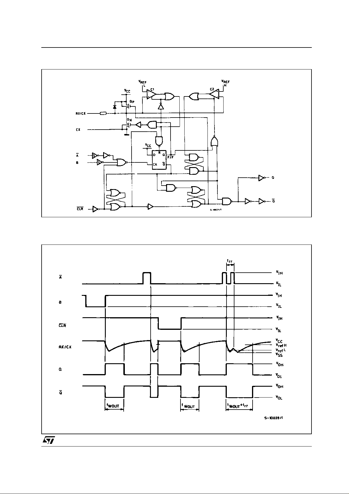
SYSTEM DIAGRAM
M74HC123
This log i c diagram has not be used to estim at e propagation delays
TIMING CHART
3/12

M74HC123
BLOCK DIAGRAM
(1) Cx, Rx , Dx are extern al components.
(2) Dx is a clamping diode.
The external capacitor is charged to Vcc in the stand-by-stat e, i.e. no trigger. When the supply vol tage is turned off Cx is discharged mainly
trough an internal parasitic diode(see figures). If Cx is sufficiently large and Vcc decreases rapidly, there will be some possibility of damaging
the I.C. with a surge current or latch-up. If the volta ge supply filter capacitor is la rge enough and Vcc decrease s l owly, the surge cu rr ent is
automatically limited and damage to the I.C. is avoided. The maximum forward current of the parasitic diode is approximately 20 mA. In cases
where Cx is large the time taken for the supply voltage to fall to 0.4 Vcc can be calculated as follows :
t
> (Vcc - 0.7) x Cx/20mA
f
In cases where t
is too short an ext ernal clamping diode is required to prot ect the I.C. from t he surge current.
f
FUNCTIONAL DESCRIPTION
STAND-BY STATE
The external capacit or,Cx, is f ully charged t o Vcc
in the stand-by state. Hence, before triggering,
transistor Qp and Qn (connected to the Rx/Cx
node) are both turned-off. The two comparators
that control the timing and the two reference
voltage sources stop operating. The t otal supply
current is therefore only leakage current.
TRIGGER OPERATION
Triggering occurs when :
1 st) A is "LOW" and B has a falling edge;
2 nd) B is "HIGH" and A has a rising edge;
3 rd) A is "LOW" and B is HIGH and C1 has a
rising edge;
After the multivibrator has been retriggered
comparator C1 and C2 start operating and Q n is
turned on. Cx then discharges through Qn. The
voltage at the node R/C external falls.
When it reaches V
the output of comparat or
REFL
C1 becomes low. This in turn reset the flip-flop
and Qn is turned off.
At this point C1 stops functioning but C2 continues
to operate.
The voltage at R/C external begins to rise with a
time constant set by the external com ponents Rx,
Cx.
Triggering the multivibrator caus es Q to go high
after internal delay due to the flip-flop and the
gate. Q remains high until the voltage at R/C
external rises again to V
. At this point C2
REFH
output goes low and O goes low. C2 stop
operating. That means that a fter triggering when
the voltage R/C external returns to V
REFH
the
multivibrator has returned to its MONOSTABLE
STATE. In the case where Rx · Cx are large
enough and the discharge time of the capacitor
and the delay time in the I.C. can be ignored, t he
width of the output pulse tw (out) is as follows :
tW(OUT) = 0.45 Cx · Rx
RE - TRIGGERED OPERATION
When a second trigger pulse follows the first its
effect will depend on the state of the multivibrator.
If the capacitor Cx i s being charged t he voltage
level of R/C external falls to V
again and Q
REFL
remains High i.e. the retrigger pulse arrives in a
time shorter than the period Rx · Cx seconds, the
capacitor charging time constant. If the second
trigger pulse is very close to the initial trigger pulse
it is ineffective ; i.e. the second trigger must arrive
in the capacitor discharge cycle to be ineffective;
Hence the minimum time for a second trigger to be
effective depends on Vcc and Cx
RESET OPERATION
CL is normally high. If CL is low, the trigger is not
effective because Q output goes low and trigger
control f lip -f lo p is res et .
Also transistor Op is turned on and Cx is charged
quickly to Vcc. This means if CL input goes low the
IC becomes waiting state both in operating and
non operating state.
4/12

M74HC123
ABSOLUTE MAXIMUM RATINGS
Symbol Parameter Value Unit
V
V
V
I
I
OK
I
I
or I
CC
P
T
T
Absolute Maximum Ratings are those values beyond which damage to the device may occur. Functional operation under these conditions is
not implied
(*) 500mW at 65
RECOMMENDED OPERATING CONDITIONS
Symbol Parameter Value Unit
V
V
V
T
t
r
Cx External Capacitor NO LIMITATION pF
Rx
The Maximum allowable values of Cx and Rx are a function of leakage of capacitor Cx, the leakage of device and leakage due to the board
layout and surface resistance. Susceptibility to externally induced noise may occur for Rx > 1MΩ
Supply Voltage
CC
DC Input Voltage -0.5 to VCC + 0.5
I
DC Output Voltage -0.5 to VCC + 0.5
O
DC Input Diode Current
IK
DC Output Diode Current
DC Output Current
O
DC VCC or Ground Current
GND
Power Dissipation
D
Storage Temperature
stg
Lead Temperature (10 sec)
L
°C; derate to 300mW by 10 m W/°C from 65 °C to 85°C
Supply Voltage
CC
Input Voltage 0 to V
I
Output Voltage 0 to V
O
Operating Temperature
op
Input Rise and Fall Time VCC = 2.0V
, t
f
V
V
CC
CC
= 4.5V
= 6.0V
External Resistor Vcc < 3V 5K to 1M
Vcc > 3V 1K to 1M
-0.5 to +7 V
± 20 mA
± 20 mA
± 25 mA
± 50 mA
500(*) mW
-65 to +150 °C
300 °C
2 to 6 V
CC
CC
-55 to 125 °C
0 to 1000 ns
0 to 500 ns
0 to 400 ns
Ω
V
V
V
V
5/12

M74HC123
DC SPECIFICATIONS
Symbol Parameter
V
V
V
V
I
I
(1) : Per Circuit
High Level Input
IH
Voltage
Low Level Input
IL
Voltage
High Level Output
OH
Voltage
Low Level Output
OL
Voltage
I
Input Leakage
I
Current
Quiescent Supply
CC
Current
Active State
CC’
Supply Current (1)
Test Condition Value
V
CC
(V)
= 25°C
A
Min. Typ. Max. Min. Max. Min. Max.
-40 to 85°C -55 to 125°C
Unit
T
2.0 1.5 1.5 1.5
6.0 4.2 4.2 4.2
2.0 0.5 0.5 0.5
6.0 1.8 1.8 1.8
2.0
4.5
6.0
4.5
6.0
2.0
4.5
6.0
4.5
6.0
6.0
6.0
2.0
4.5 500 600 780 960 µA
6.0 0.7 1 1.3 1.6 mA
IO=-20 µA
I
=-20 µA
O
I
=-20 µA
O
I
=-4.0 mA
O
I
=-5.2 mA
O
IO=20 µA
I
=20 µA
O
I
=20 µA
O
I
=4.0 mA
O
I
=5.2 mA
O
= VCC or GND
V
I
= VCC or GND
V
I
V
= VCC or GND
I
Pin 7 or 15
V
= VCC/2
IN
1.9 2.0 1.9 1.9
4.4 4.5 4.4 4.4
5.9 6.0 5.9 5.9
4.18 4.31 4.13 4.10
5.68 5.8 5.63 5.60
0.0 0.1 0.1 0.1
0.0 0.1 0.1 0.1
0.0 0.1 0.1 0.1
0.17 0.26 0.33 0.40
0.18 0.26 0.33 0.40
± 0.1 ± 1 ± 1 µA
44080µA
45 200 260 320 µA
V4.5 3.15 3.15 3.15
V4.5 1.35 1.35 1.35
V
V
6/12

AC ELECTRICAL CHARACTERISTICS (CL = 50 pF, Input tr = tf = 6ns)
Test Condition Value
T
Symbol Parameter
t
TLH tTHL
t
PLH tPHL
t
PLH tPHL
Output Transition
Time
Propagation Delay
Time
, B - Q, Q)
(A
Propagation Delay
Time(CLR
TRIGGER - Q, Q)
t
PLH tPHL
t
WOUT
∆t
WOUT
Propagation Delay
Time
- Q, Q)
(CLR
Output Pulse Width 2.0
Output Pulse Width
Error Between
Circuits in Same
Package
t
W(H)
t
W(L)
t
W(L)
Minimum Pulse
Width
Minimum Pulse
Width (CLR
Minimum Retrigger
t
rr
Time
)
V
CC
(V)
2.0 30 75 95 110
6.0 7131619
2.0 102 210 265 315
6.0 22 36 45 54
2.0 102 235 295 355
6.0 23 40 50 60
2.0 68 160 200 240
6.0 16 27 34 41
Cx = 100 pF
6.0 1.1
2.0
6.0 4.3
Rx = 10K
Cx = 0.1µF
Rx = 100K
Ω
Ω
2.0 75 95 110
6.0 13 16 19
2.0 75 95 110
6.0 13 16 19
2.0
6.0 78
2.0
6.0 1.2
Cx = 100 pF
Rx = 10K
Ω
Cx = 0.1µF
Rx = 100K
Ω
= 25°C
A
Min. Typ. Max. Min. Max. Min. Max.
1.4
4.6
±1
325
5
M74HC123
-40 to 85°C -55 to 125°C
Unit
ns4.5 8151922
ns4.5 29 42 53 63
ns4.5 31 47 59 71
ns4.5 20 32 40 48
µs4.5 1.2
ms4.5 4.4
%
ns4.5 15 19 22
ns4.5 15 19 22
ns4.5 108
µs4.5 1.4
CAPACITIVE CHARACTERISTICS
Test Condition Value
T
Symbol Parameter
V
CC
(V)
C
C
1) CPD is defined as the value of the IC’s internal equivalent capacitance which is calculated from the operating current consumption without
load. (Refer to Test Circuit). Average operating current can be obtained by the following equation. I
+ Ic/2(per monostable) (I
Input Capacitance
IN
Power Dissipation
PD
Capacitance (note 1)5.0 162 pF
’ : Active Supply current) (Duty : %)
cc
5.0 5101010pF
= 25°C
A
Min. Typ. Max. Min. Max. Min. Max.
-40 to 85°C -55 to 125°C
= CPD x VCC x fIN + ICC’ Duty/100
CC(opr)
Unit
7/12

M74HC123
TEST CIRCUIT
CL = 50pF or equivalent (includes jig and probe capacitance)
= Z
R
WAVEFORM : SWITCIHNG CHARACTERISTICS TEST WAVEFORM (f=1MHz; 50% duty cycl e)
of pulse generator (typically 50Ω)
T
OUT
8/12

M74HC123
Plastic DIP-16 (0.25) MECHANICAL DATA
mm. inch
DIM.
MIN. TYP MAX. MIN. TYP. MAX.
a1 0.51 0.020
B 0.77 1.65 0.030 0.065
b 0.5 0.020
b1 0.25 0.010
D 20 0.787
E 8.5 0.335
e 2.54 0.100
e3 17.78 0.700
F 7.1 0.280
I 5.1 0.201
L 3.3 0.130
Z 1.27 0.050
P001C
9/12

M74HC123
SO-16 MECHANICAL DATA
DIM.
A 1.75 0.068
a1 0.1 0.2 0.003 0.007
a2 1.65 0.064
b 0.35 0.46 0.013 0.018
b1 0.19 0.25 0.007 0.010
C 0.5 0.019
c1 45° (typ.)
D 9.8 10 0.385 0.393
E 5.8 6.2 0.228 0.244
e 1.27 0.050
e3 8.89 0.350
F 3.8 4.0 0.149 0.157
G 4.6 5.3 0.181 0.208
L 0.5 1.27 0.019 0.050
M 0.62 0.024
S8° (max.)
MIN. TYP MAX. MIN. TYP. M AX.
mm. inch
10/12
PO13H

M74HC123
TSSOP16 MECHANICAL DATA
mm. inch
DIM.
MIN. TYP MAX. MIN. TYP. M AX.
A 1.2 0.047
A1 0.05 0.15 0.002 0.004 0.006
A2 0.8 1 1.05 0.031 0.039 0.041
b 0.19 0.30 0.007 0.012
c 0.09 0.20 0.004 0.0089
D 4.9 5 5.1 0.193 0.197 0.201
E 6.2 6.4 6.6 0.244 0.252 0.260
E1 4.3 4.4 4.48 0.169 0.173 0.176
e 0.65 BSC 0.0256 BSC
K0° 8°0° 8°
L 0.45 0.60 0.75 0.018 0.024 0.030
A2
A
A1
b
e
c
K
L
E
D
E1
PIN 1 IDENTIFICATION
1
0080338D
11/12

M74HC123
Information furnished is bel ieved to be accurate and reliable. However, STMicroe lectronics assumes no responsibility for the
consequences of use of such information nor for any infringement of patents or other rights of third parties which may result from
its use. No li cense is granted by imp lication or otherwise under any patent or patent rig hts of STMicroelectronics. Specifications
mentioned in this publication ar e subject to change without notice. This publication supersedes and replaces all information
previously supplied. S TMicroelectronics products are not authorized for use as critica l components in life suppo rt devices or
systems without express written approval of STMicroelectronics.
Australi a - Brazil - China - Finland - France - Germany - Hong Kong - India - Italy - Japan - Malaysi a - Malta - Morocco
© The ST logo is a registered trademark of STMicroelectronics
© 2001 STM icroelectronics - Prin ted in Italy - A ll Rights Reser ved
STMicr o el ectronics GROUP OF COMPANIES
Singapo re - Spain - Swe den - Switzerl and - United K i ngdom
© http://www.st.com
12/12
 Loading...